Comprehensive Design and Analysis of a State-Feedback Controller for a Dynamic Voltage Restorer
by
 ,
,
Javier Roldán-Pérez
1,*,† ,
,
Aurelio García-Cerrada
2,†,
Alberto Rodríguez-Cabero
1,† and
Juan Luis Zamora-Macho
2,† 1
IMDEA Energy Institute, 28935 Mostoles, Spain
2
Universidad Pontificia Comillas, ICAI-School of Engineering, Instituto de Investigación Tecnológica (IIT), 28015 Madrid, Spain
*
Author to whom correspondence should be addressed.
†
These authors contributed equally to this work.
Energies 2018, 11(8), 1972; https://doi.org/10.3390/en11081972
Submission received: 31 May 2018
/
Revised: 12 July 2018
/
Accepted: 28 July 2018
/
Published: 30 July 2018
(This article belongs to the Section I: Energy Fundamentals and Conversion)
Abstract
:Voltage sags result in unwanted operation stops and large economical losses in industrial applications. A dynamic voltage restorer (DVR) is a power-electronics-based device conceived to protect high-power installations against these events. However, the design of a DVR control system is not straightforward and it has some peculiarities. First of all, a DVR includes a resonant (LC) connection filter with a lightly damped resonance. Secondly, the control system of a DVR should work properly regardless of the type of load, which can be linear or non-linear, to be protected. In this paper, a digital state-feedback (SF) controller for a DVR is proposed to address these issues. The design and features of the SF controller are studied in detail. Two pole-placement alternatives are discussed and the system robustness is tested under variations in the system parameters. Furthermore, implementation aspects such as discretization not commonly addressed in the literature are described. The controller is implemented in its incremental form. A decoupling system for the dq-axis dynamics that takes into account system delays and the load current is proposed and analytically studied. The proposed controller is compared with two other alternatives found in the literature: a Proportional-Integral-Differential (PID) controller and a cascade controller. The effect of the load connected downstream a DVR is also studied, revealing the potential of the SF controller to damp the resonance under light load conditions. All control system developments were tested in a 5 kVA prototype of a DVR connected to a configurable grid.
1. Introduction
Most downtimes in industry are due to voltage sags [1]. Unfortunately, it is difficult to immunize equipment against these voltage events and, if the sag lasts for a long time, equipment shutdown is inevitable. Uninterruptible power supplies (UPSs) are often used for protecting sensitive loads against voltage sags [2]. UPSs are widely applied to protect low-power loads such as computers or small electronic loads. They replace the grid when a voltage sag takes place and, when the voltage level recovers, loads are gently reconnected to the grid. However, a UPS has to deliver all the power consumed by the protected loads during a sag. This means that a UPS requires large batteries to protect loads against long-duration voltage sags and, consequently, its application is greatly restricted by the size and cost of batteries. A dynamic voltage restorer (DVR) is conceived to protect sensitive loads against voltage sags and swells. This device is connected in series with an electrical distribution line and, typically, it consists of a voltage source converter (VSC), a DC capacitor, a coupling transformer, batteries, and an AC filter [3]. When a voltage sag takes place, a DVR injects the required voltage in series with the feeding line and the load voltage remains unchanged [4]. The main advantage of DVRs is that only a portion of the power consumed by the load is supplied from the batteries. This means that batteries can be made much smaller than in a typical UPS and cost can be reduced. These reductions in battery size and cost make DVRs very attractive for high-power applications where a UPS may be infeasible. Antchev et al. [5] presented a series-connected power-electronics device that was able to restore the voltage of a load under distorted grid conditions. A bidirectional AC–DC converter was used to maintain the DC voltage constant so that no additional energy storage elements were required.
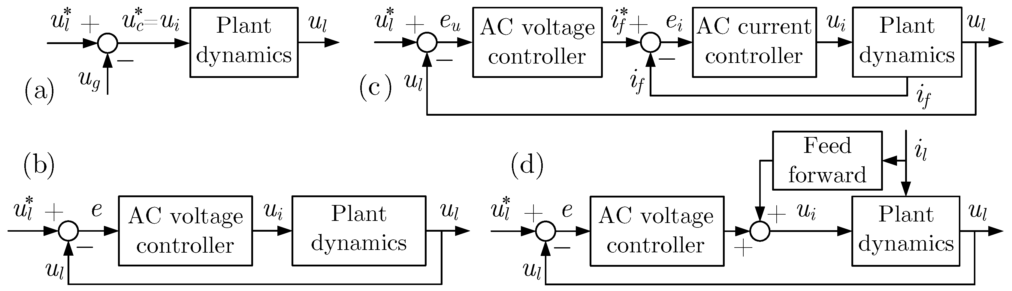
The main task of a DVR is to control the load voltage. Therefore, a control scheme is commonly adopted. DVRs are sometimes controlled by using open-loop techniques, as shown in Figure 1a, where is the load voltage, is the series-injected voltage, is the converter output voltage, and “∗” marks reference values. Stability is guaranteed with this control technique if the plant is stable (always the case for a DVR). However, the system performance deteriorates when there are disturbances. Open-loop control has clear drawbacks:
Open-loop control techniques were applied by Jimichi et al. [8] to control a DVR, obtaining a fast transient response. However, performance was poor if the AC filter included a capacitor because of the filter resonance [9,10,11]. In most cases, DVRs are controlled by using a feedback control scheme like the one depicted in Figure 1b [12,13,14], where e is the system control error (). Additionally, the current consumed by the sensitive load can be added as a feed-forward signal, as shown in Figure 1d [12]. Feedback control provides accurate reference tracking provided the closed-loop plant is stable. However, DVR feedback control can be difficult because (a) the load modifies the plant dynamics and (b) the LC filter resonance is difficult to damp with a controller based on a single loop [15].
The DVR control system can be implemented in a synchronous reference frame (SRF) [16], a static reference frame (RF) [17], or in natural magnitudes () [11]. If the controller is applied in natural magnitudes or in a stationary RF (), decoupling equations are not required. However, a resonant controller is needed to achieve zero steady-state error for the fundamental component [17]. By far, the most common alternative is to use an SRF because the fundamental components of all magnitudes are constant values in steady state [18]. Therefore, a proportional-integral (PI) controller is enough to track balanced voltage sags, although the -axis dynamics are coupled. In addition, a phase-locked loop (PLL) is needed to synchronize the SRF with the grid voltage [18]. An alternative controller was presented by Badrkhani Ajaei et al. [19]. This alternative was implemented by using time-varying phasors that did not require a PLL and made it possible to independently control each phase. However, the transient response was slower when compared to other control algorithms because the phasors needed to be estimated.
The simplest solution to damp the resonance is to add a resistor close to the AC capacitor, but this increases losses. A multi-loop control scheme like the one depicted in Figure 1c is a classical solution to damp resonances: first, the current through the filter inductor () is controlled by the inner AC-current controller, and, secondly, the load voltage () is controlled by the AC-voltage controller. With this control scheme, the resonance can be actively damped and no extra passive elements are required [15]. Nevertheless, extra measurements are required. A DVR can also be controlled by using a single control loop. For instance, Goharrizi et al. [11] controlled a DVR with an LC filter by applying a PID controller and a fast transient response with a reduced overshoot was obtained. However, the load voltage quality deteriorated when loads were non-linear. Alternatively, Roncero-Sánchez et al. [20] damped the resonance by applying a PI controller plus a notch filter tuned at the resonant frequency: the notch filter simplified the PI controller design, but the result was not robust against variations in the system parameters. A Posicast controller is another alternative to damp resonances with a single loop, as shown by Hung [21]. This type of controller is simple to design and implement, and it was applied to control a DVR by Mahdianpoor et al. [22]. However, a Posicast controller leads to poor results when the system dynamics are not accurately known. Alternatively, Petkova et al. [23] and Antchev et al. [24] presented a fast sliding-mode controller for a series active power filter (SAPF) that protected a load against voltage harmonics. The main advantage of this controller was robustness against variations in the system parameters, and this feature is of interest for its application to a DVR. Other control options, like hystheresis controllers, can also be found in the literature [25,26,27]. Artificial-intelligent techniques have also been applied to a DVR to compensate for voltage sags: fuzzy logic was applied by Teke et al. [28], while neural networks were applied by Jurado [29] and by Elnady and Salama [30]. In addition, Saleh et al. [31] applied wavelets to control a DVR by using a multi-loop control strategy, obtaining a fast transient response. However, these alternatives are not very popular because their design is not straightforward and their performance is difficult to predict. The so-called “virtual resistor” control technique can be used to actively damp LC filter resonances by emulating the dynamic behavior of a resistor with an inner current loop [15]. Loh et al. [32] and Blasko and Kaura [33] studied several multi-loop control strategies to damp resonances, concluding that a DVR is less sensitive to current harmonics if the capacitor current is used as the inner control variable.
The resonance in a DVR can be also damped by using a state-feedback (SF) controller and placing closed-loop poles in appropriate locations, as shown by Cheng et al. [34]. This type of controller is straightforward to design, but it is sometimes difficult to figure out how closed-loop poles should be placed to have acceptable stability margins. Alternatively, Hasanzadeh et al. [35] selected the controller gains of a UPS by using a linear quadratic regulator (LQR) in order to optimize the transient response. Addressing the problem in this way, the position of closed-loop poles is no longer a problem; however, the value of the weighting gains for the LQR problem may be difficult to find. In that work, the LQR problem was solved in continuous time, and discrete-time effects were not taken into account. Huerta et al. [36] designed the controller gains of a VSC with an LCL filter by solving the LQR problem, with accurate results. A similar approach was applied by Ochoa et al. [37] for a Universal Power Quality Conditioner (UPQC). A basic SF controller for DVRs was applied in our previous work [38]. However, in that work, the SF controller was not explained, and the effect of delays was not considered in the decoupling equations. Additionally, neither pole-placement alternatives nor system robustness was studied, and these topics is addressed in detail in this paper. Further contributions of this paper include: a detailed description of the design and implementation procedures, a detailed analysis of stability issues, an analysis of the load effect, and a comparative study.
In this paper, an SF controller for a DVR is proposed. Design and controller features are comprehensively studied. Implementation aspects such as discretization, which are not commonly addressed in the literature, are described and explained. A novel decoupling strategy that minimizes the coupling between the dq-axis dynamics, taking into account the system delays, is proposed. Additionally, two alternatives to place the closed-loop poles are studied. With the first one, a dominant pole is selected manually, while, with the second one, the poles are placed by solving the LQR problem. The robustness of the closed-loop system against variations in the system parameters is studied in detail. The controller is implemented in its incremental form to simplify practical issues such as saturation. To highlight the potential of the proposed controller, it is compared with two other alternatives found in the literature: a PID controller and a cascade controller. The comparative analysis is made both theoretically and practically. The effect of the load connected downstream the DVR is also studied. It is shown that the SF controller provides fast transient responses and an adequate damping of the LC filter resonance despite load variations. The main features of the controller were tested in a 5 kVA prototype of a DVR connected to a grid emulator.
2. DVR Modeling and Control
2.1. DVR Overview
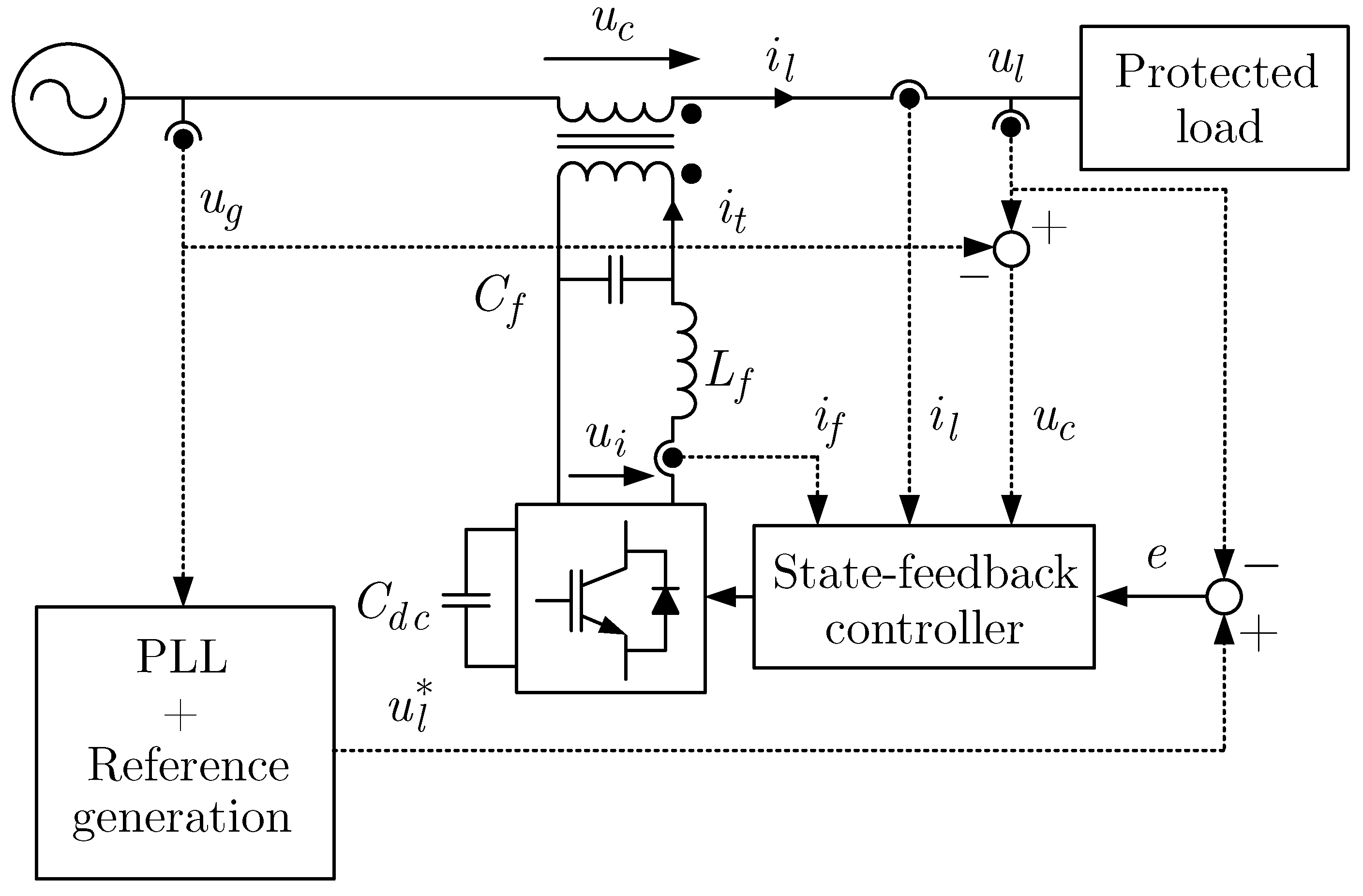
A DVR is depicted in Figure 2. The VSC is connected in series with the Point of Common Coupling (PCC) by using an filter ( and ) and a coupling transformer (leakage inductance is called and copper losses are modeled with ). The DC-link capacitor is called .
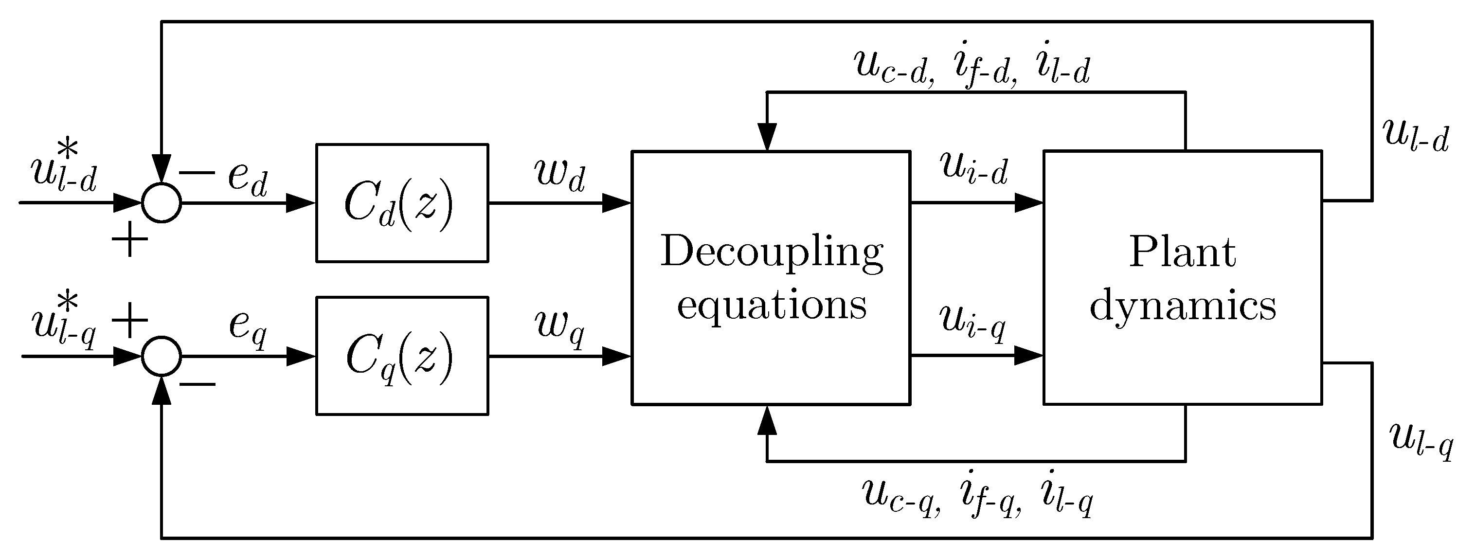
Figure 3 shows the structure of the control system proposed for a DVR. Electrical system dynamics are represented by the block called “plant dynamics.” Space vectors will be marked with a right arrow over the variable name (e.g., ), and, to simplify Figure 3 and others, the time dependence of signals will be purposely omitted in most of them. Subscripts d and q stand for the direct axis and quadrature axis, respectively. Park’s transformation will be used to refer all electrical variables to a reference frame that rotates synchronously with the d-axis component of the grid voltage space vector (). This reference frame will be called “synchronous reference frame” (SRF), and it is chosen to force , so . Therefore, d- and q-axis dynamics will be coupled and a set of decoupling equations is required to design independent controllers for each axis [39].
2.2. Per-Unit Model
Per-unit (pu) models simplify the implementation of control algorithms in Digital Signal Processors (DSPs). There are many approaches to select base values depending on the application [40]; however, in this paper, base values for the three-phase voltages and currents have been chosen so that rated voltages and currents of the device produce unit-magnitude vectors when referred to an SRF. These base values are summarized in Table 1, where is the phase-voltage rotation between the primary side (VSC) and the secondary side (grid) of the coupling transformer, and is the conversion ratio (1:). All base values are referred to the grid side of the coupling transformer [18]. Subscript b stands for base and subscript n stands for nominal.
Some important remarks regarding the information displayed in Table 1 are as follows:
- The peak value of nominal three-phase (sinusoidal) signals is after dividing them by their base value. Therefore, for the rest of the paper, three-phase waveforms are drawn multiplied by so that their peak value at nominal conditions is 1 pu.
However, when designing and implementing controllers no base frequency will be used (numerically is like if ) because it is easier to interpret designs by using natural dimensions (hertz or seconds) rather than per-unit. For the rest of the paper, results will be shown in per-unit values unless otherwise stated.
2.3. Continuous-Time Modeling
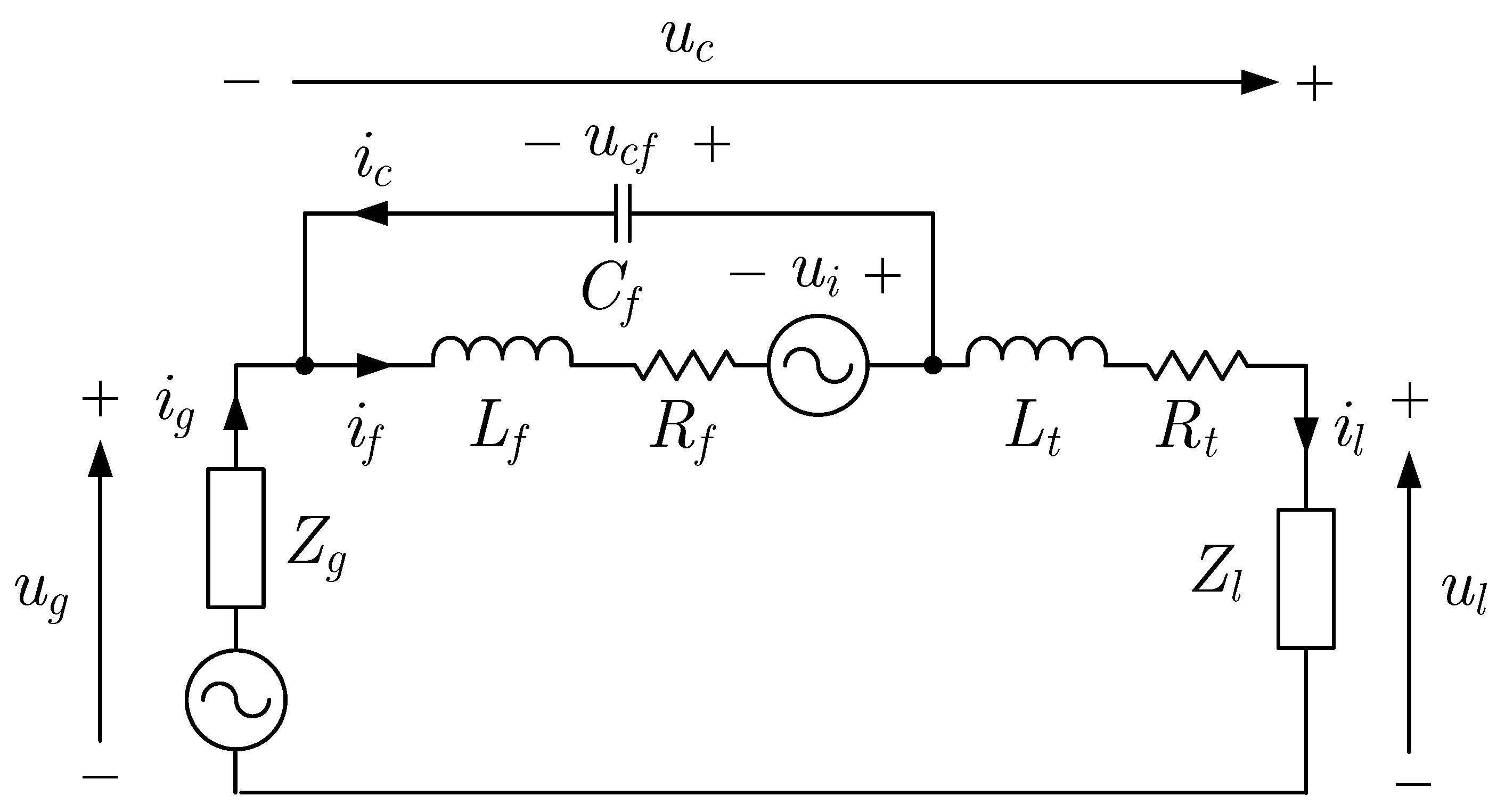
This section briefly summarizes the model of the DVR in continious time [38]. A single-phase equivalent for a DVR is depicted in Figure 4. The grid impedance is modeled as and its current is . The sensitive load current is . The filter inductor is modeled with and . The model of the transformer includes the leakage inductance and the copper resistance . The transformer current is . The filter capacitor is , is its voltage, and its current. Since all variables are in pu, there is no need to include the transformer conversion ratio. The model of the transformer is , and it is connected in series with the model of the load, , where . Since, typically, the voltage across the filter capacitor is very similar to the output voltage of the DVR, . Therefore, the DVR model can be written as
with
where all electrical variables are represented by space vectors of components in per-unit after applying Park’s transformation [39]. The control system output is , is a disturbance, and is the synchronous frequency. Subscript t in and highlights the time dependence of signals.
2.4. Discrete-Time Model
This section briefly summarizes the model of the DVR in discrete time [38]. The equivalent discrete-time model is obtained by applying the zero-order hold (ZOH) method to the system in Equation (1), yielding [38,42]:
where
The sampling period is . By separating the -axis dynamics, Equation (4) can be written as follows:
where
The control outputs are and , the state variables are and , and and are disturbances. The subscript k indicates the discrete-time sample of a continuous-time signal. In order to control the system dynamics with independent controllers (one for each axis, d and q), the state-space model in Equation (6) can be rewritten in terms of two “desired” virtual control outputs ( and ). These control outputs guarantee that the -axis dynamics are perfectly decoupled. However, perfect decoupling will not be obtained in this paper and the “actual” virtual control outputs, to be called and , will be calculated so that coupling terms are minimized.
Therefore, the desired -axis dynamics can be written as
where 0 is a matrix full of zeros of the appropriate size. The actual control output can be calculated by equating the right-hand-side terms of Equation (6) and Equation (9), yielding
From Equation (10), the value and can be calculated in terms of and , the state variables, and the disturbances. However, perfect decoupling is not possible in this situation since the set of equations in Equation (10) has more equations than variables to solve. Therefore, the “desired” virtual control output is replaced by the “actual” virtual control output (which does not guarantee perfect decoupling), to be mathematically consistent. One possible solution for and is
where is the left pseudo-inverse matrix of :
and t means “transposed.” The solution presented in Equation (11) minimizes the coupling terms between the -axis dynamics because it is obtained by using the pseudo-inverse matrix, and this provides the least-squares solution of Equation (10).
2.5. Plant Model with Delays
For control purposes, the accuracy of plant model improves if the calculus delay and the delay caused by the anti-aliasing filters are included in the discrete-time model [43]. The former is naturally modeled by a one-sample delay in the control output. The latter can also be modeled by a one-sample delay in the control output if the appropriate Bessel filters are used for all measurements [40]. The output calculated by the controller is , where stands for “advanced.” The new state variables that model the virtual control outputs and their advanced versions must be included in the state-space model. Therefore, the following variables are defined:
Notice that delays have been modeled directly in the SRF, although they are produced in and they generate a coupling effect when referred to an SRF. However, these coupling effects can be compensated when conditioning the converter output voltage [41].
The discrete-time model of the plant in Equation (9) plus the delays can be written as (only the d-axis shown)
The controller will calculate , which is the input of the plant model (15) in k. Calling to the actual VSC voltage to be applied in , the decoupling equations with delays can be derived from Equation (11), yielding
Clearly, the values of (to be applied in ) in Equation (16) depend on the state variables and the load current at the instant , which are not available at the instant k. However, the value of can be predicted two steps ahead and replaced in Equation (16) by using the approach presented by García-Cerrada et al. [43,44], yielding
where the “hat” refers to “predicted.” In addition, assuming the load current varies slowly, , so the decoupling equations in Equation (16) can be readily applied.
2.6. Control Problem Definition
The SF controller presented in this paper is used to control the load voltage () by manipulating the VSC output voltage (). To simplify the design of the control system, virtual control outputs are used (). This makes it possible to design independent controllers for each axis. Since the fundamental component of the grid voltage becomes a constant value when Park’s transformations are applied, integral controllers are required to guarantee zero steady-state error. Controlling the load voltage is a challenging control problem since the filter introduces a lightly damped resonance into the system. Additionally, the LC filter resonance is close to the Nyquist frequency since the switching frequency is relatively slow due to technical limitations.
3. State-Feedback Controller
3.1. Integral State-Feedback Controller
Integrals for the errors of the output variables () can be easily added to the state-space model, yielding [43,45]
Therefore, the open-loop equations for the d-axis are (similar for the q-axis):
and the controller will calculate
while the actual values of the control output are computed with Equation (16). The gains and are row vectors that contain the controller gains for the d- and q-axis controllers, respectively. These gains can be designed by using any pole-placement algorithm [43,45].
The system in Equation (19) is controllable if the rank of equals the number of state variables. Since variations in hardware elements are common in power electronics applications, the system controllability was checked for this possible situation. Variations in , , and of % were considered. Additionally, the test was carried out for variations in the grid frequency of %. The rank of calculated with Matlab was always five regardless of the value of the parameters. Therefore, the system can be considered controllable.
3.2. Incremental Controller
The initial connection to the grid might cause large variations in the control outputs and oscillations in the controlled variables. This can be avoided by using incremental controllers [47]. For this purpose, the control system output can be rewritten as follows:
and the incremental part of the control output is computed as
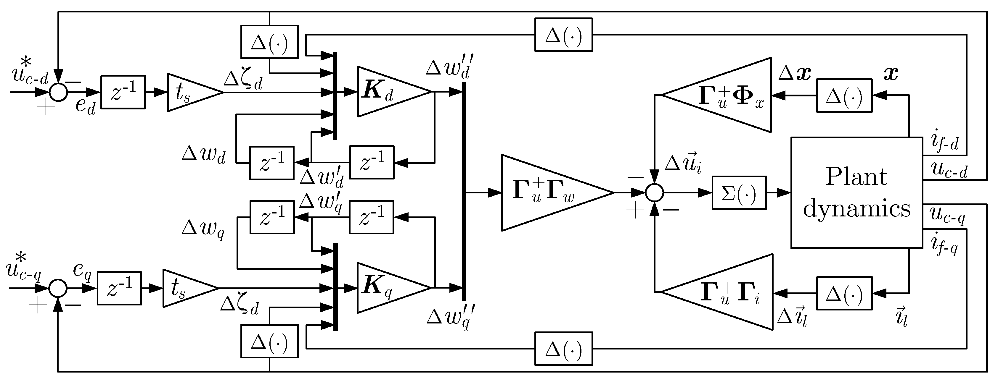
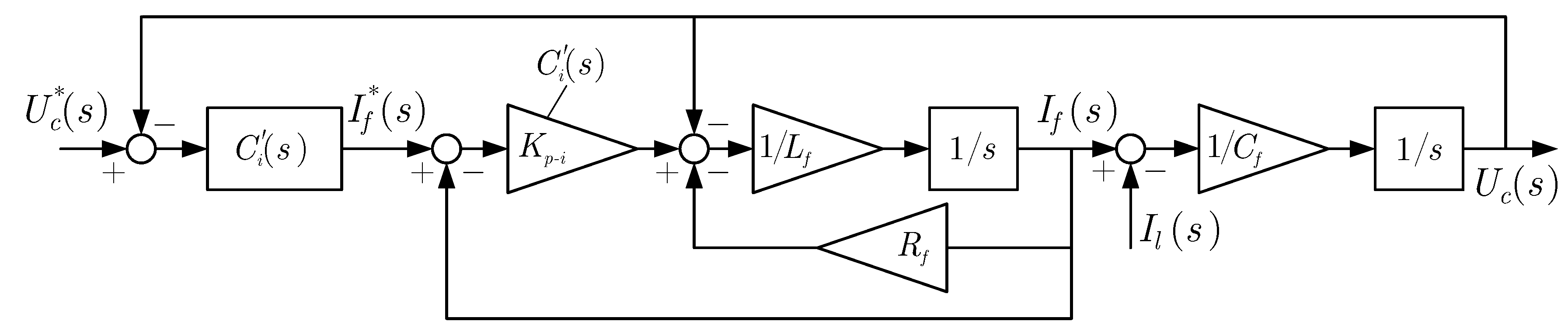
where stands for the incremental operator. Figure 5 shows the implementation of the SF controller in its incremental form. Addressing the problem in this way, the implementation of an anti-windup mechanism becomes trivial because is added to the control output only if falls within operation limits [47]. Incremental implementation is especially useful if the controller includes integrals because these are moved to the control system output.
4. Prototype Description
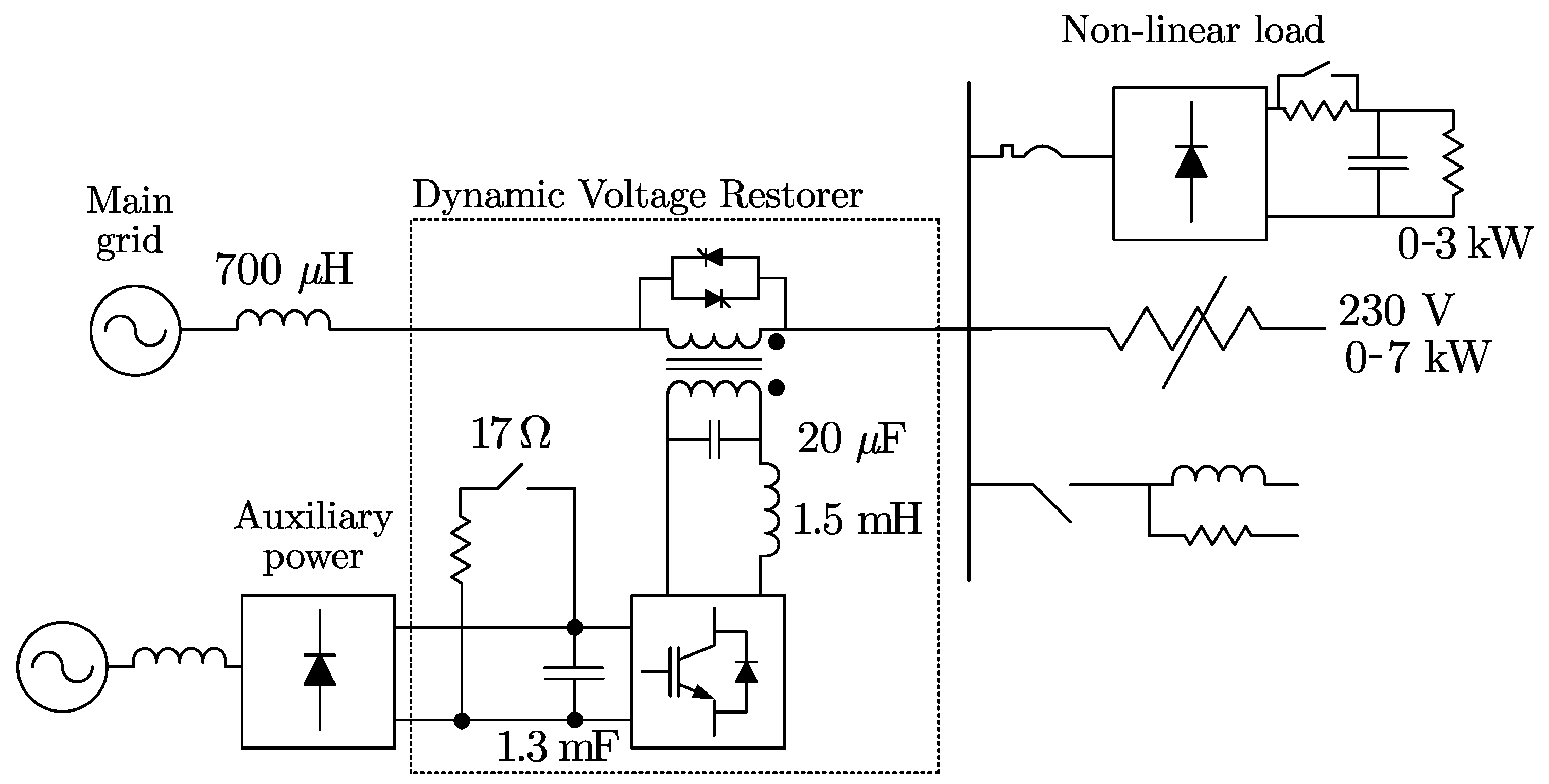
The laboratory test-rig used throughout this work is depicted in Figure 6 and Figure 7. The nominal line-to-line voltage at the PCC was set to 230 V (phase-to-phase) and 50 Hz. The grid was emulated with an AMX-Pacific 3120 (Pacific Power Source, Inc., Irvine, CA, USA)12 kVA three-phase voltage source that was used to generate voltage sags. The line impedance was emulated with an inductor of H and m rated at 30 A. The DVR consisted of a 2-level 3-leg Insulated Gate Bipolar Transistor (IGBT)-based VSC based on the commercial package SKS22F B6U (SEMIKRON GmbH, Nuremberg, Germany). This package provides a VSC, a diode rectifier, a DC capacitor (1.3 mF, 750 V), a DC–DC converter (“braking chopper”), and a soft-charge circuit. A resistor of 17 (maximum of 10 kW in 10 s, or 1 kW continuously) was used together with the DC–DC converter to protect the DVR in case of DC overvoltage.
Loads were connected downstream the DVR using a manual breaker. The load used consisted of a linear and a non-linear load. The standard load used for the tests consumed 3 kW and 2 kvar at rated voltage (0.88 power factor). The non-linear load consisted of a diode rectifier with a soft-charge circuit. The DC-side of the load could be used with an inductive or a capacitive filter.
The series-coupling transformer was a 6 kVA three-phase transformer with unity turn ratio (190 V:190 V) and Ynz11 connection. This connection, although it is not very common, is very efficient redistributing the current through the windings when the protected load consumes unbalanced currents. The Y side of the transformer was connected to the VSC. This transformer had a series resistance and a leakage inductance of and mH, respectively. The filter capacitor value was F and the filter inductor was mH. Therefore, the resonance frequency of the filter was 918 Hz. When the DVR was not connected to the grid, it was bypassed using three independent solid-state relays (SSR) rated at 400 V and 30 A (see [38] for more details).
Currents were measured with current sensors LEM LA25-NP (1 mA/1 A, LEM International S.A., 1228 Plan les Ouates, Switzerland) with one turn, while voltages were measured with voltage sensors LEM LV25-P (500 V, same manufacturer). All measurements were filtered with low-pass filters before the data acquisition system. The filters were selected as fifth-order Bessel’s filters with 2600 Hz cut-off frequency and they were implemented by using the integrated circuit LT1065 (Linear Technolgy, Milpitas, CA, USA). The operational amplifiers AD8031AN (Analog Devices, Norwood, Mass. USA) and AD8032AN (same manufacturer) were used to improve the signal-to-noise ratio before measuring with the Analog-to-Digital Converters (ADCs). The Bessel’s filters mentioned above were approximated by one-sampling-period delay in each measured signal, so they can easily be taken into account in the controller designs [43].
The platform dSPACE DS1103 (dSPACE, GmbH, Paderborn, Germany) was used to run the control algorithms and to generate the Pulse-Width Modulation (PWM) signals for the VSC and the DC-DC converter. The control system was developed in a PC by using MATLAB R2010b and Simulink (Mathworks Natick, Mass., USA). The control algorithms were tested first in simulation and then compiled and downloaded to the DSP by using a compiler provided by dSpace. The DSP was connected to the PC by using a high-speed fiber-optic link, thanks to which a large number of variables could be stored simultaneously in real time. The visualization and capture of results were done with ControlDesk v5.5, which was included with the dSpace platform. The PWM calculations were carried out in an slave DSP TM320F240, which is included in the platform. The sampling and switching frequencies were 5.4 kHz.
The dSpace platform gave access to a variable, called turnaroundTime, that contained the execution time of the whole control system for each sampling period. In order to obtain an averaged value of the execution time, a moving-average filter of 108 samples (1 grid cycle) was applied to the measured value. After this calculation, the average execution time was 101.8 s.
5. Application of an SF Controller to a DVR
5.1. Closed-Loop Pole Position
5.1.1. Simple Pole-Placement Alternative
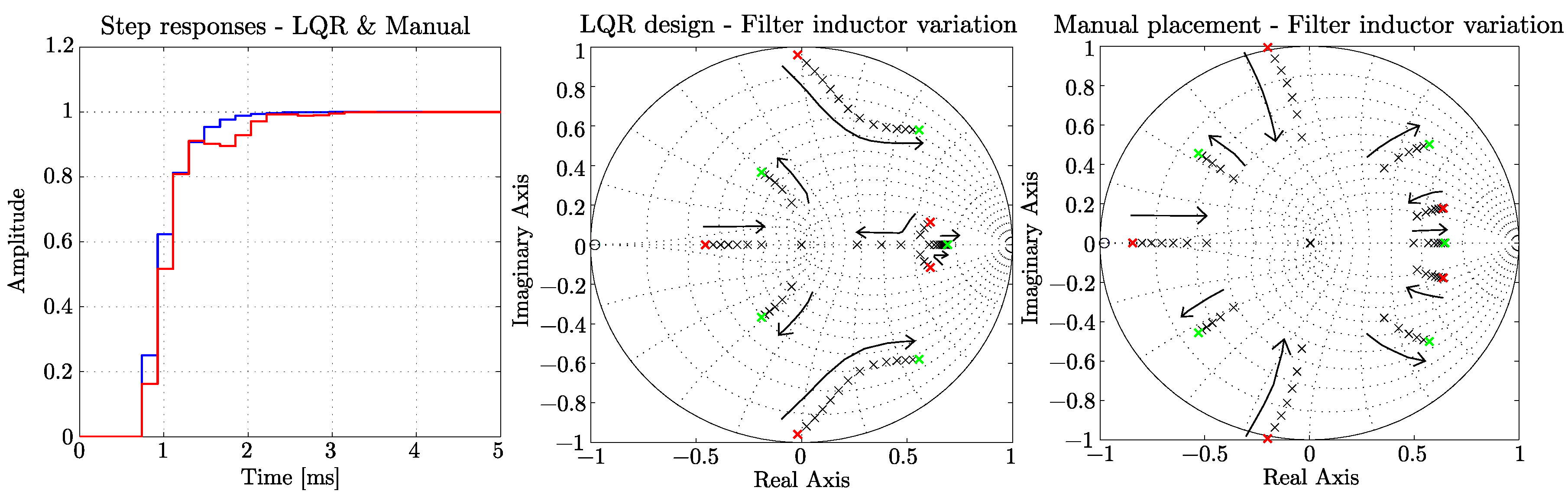
A simple alternative is to place the closed-loop poles (same approach for both axes) as follows: a dominant real pole below the resonance frequency ( rad/s), while all other poles can be made real and placed at high frequency ( rad/s). The gain vectors calculated by the pole-placement algorithm are and in Figure 5. It was found that high-frequency poles (the ones located at 2500 Hz) had an important effect over stability margins. Details regarding robustness will be discussed later in Section 7.
5.1.2. Pole-Placement by Solving the LQR Problem
With this pole-placement alternative, the closed-loop pole position is chosen in order to minimize a specific cost function, and it is commonly known as LQR [48]. This alternative produces robust controllers and it is an adequate choice for power electronics converters [37,49].
The gain of the SF controller is obtained by minimizing the following index:
where superscript means transposed, while and are weighting matrices that are used to tune the controller. Detailed information regarding the design procedure can be found in [36,37], and it is not included here for simplicity. For the scope of this paper, the transient speed of both alternatives (LQR and manual placement) was made similar.
5.1.3. Comparative Analysis of the Pole-Placement Alternatives
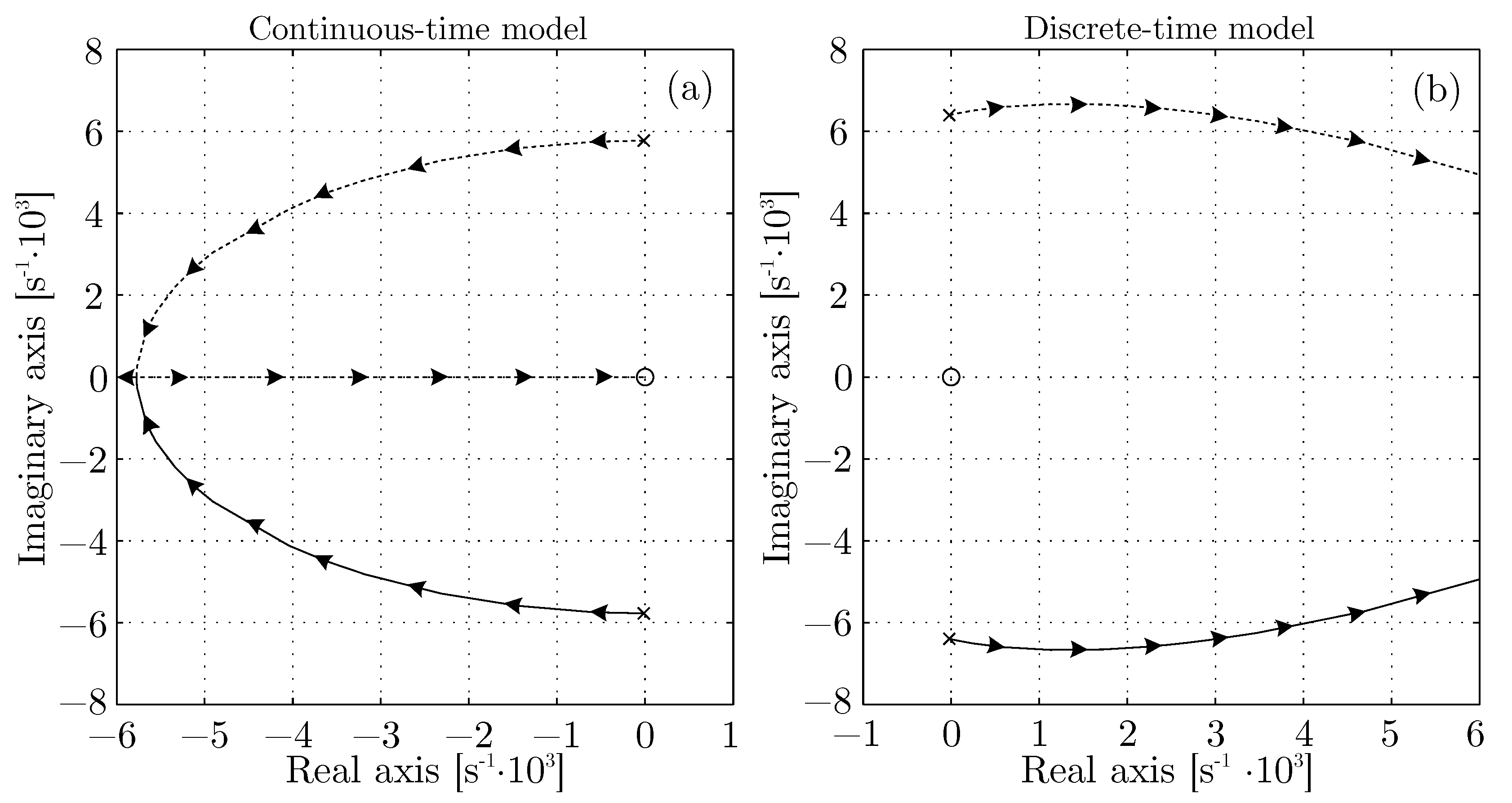
Figure 8 shows the transient and the closed-loop pole position for the two pole-placement alternatives. In both cases, the transient speed was made similar, as shown in Figure 8 (left). The value of the filter inductor () was modified in order to quantify the system robustness against variations in the parameters. For a variation of % in its value, the closed-loop system obtained by manual pole placement became unstable (see Figure 8, right). However, for the design based on the LQR controller the system remained stable. Clearly, for similar performance, the LQR alternative produced more robust controllers.
5.2. Closed-Loop System Analysis
The closed-loop system can be written as
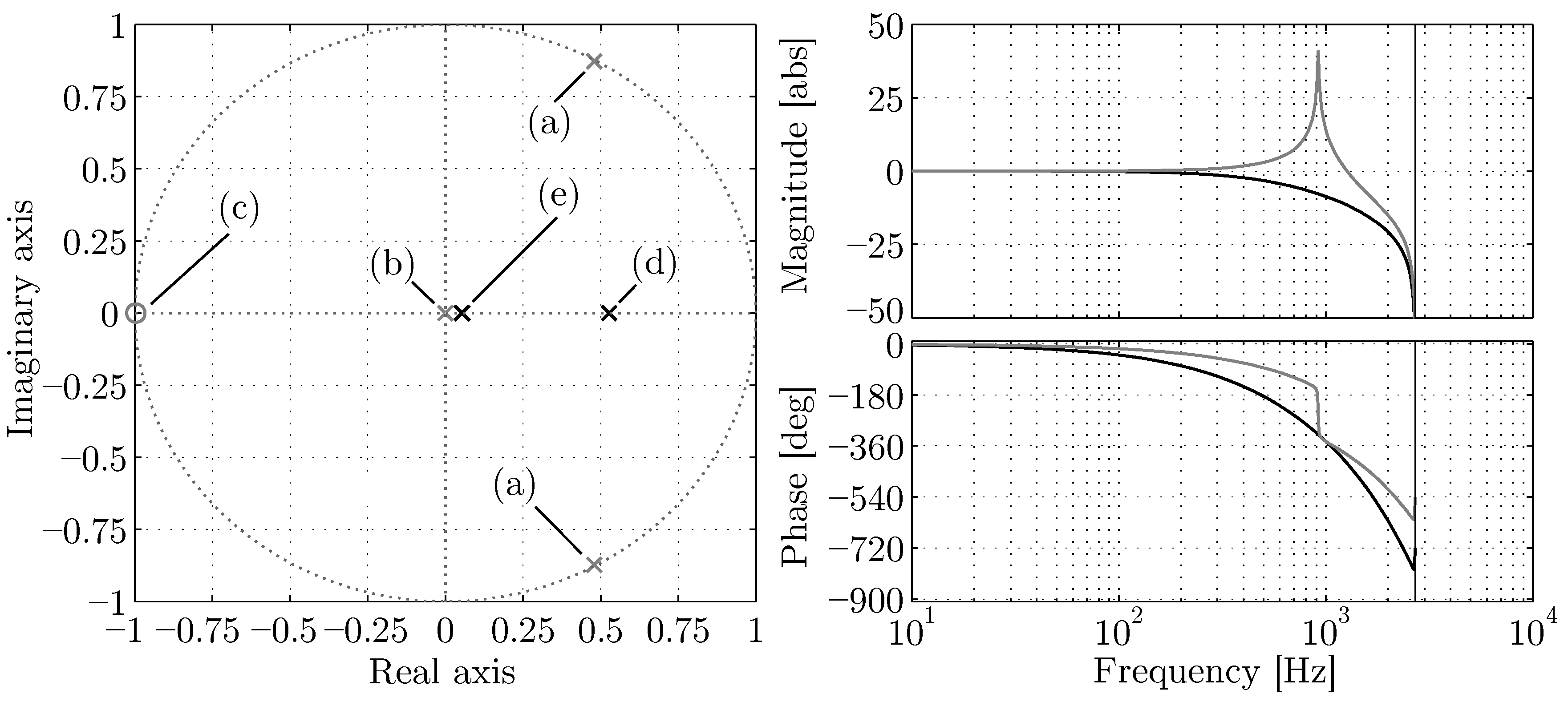
Figure 9 (left) compares the pole (×)-zero map of the plant (in grey) and of the compensated plant (in black). Meanwhile, Figure 9 (right) compares the frequency response of the plant (in grey) with the one of the closed-loop system (in black). The poles of the closed-loop system consist of (a) the poles related to the filter resonance, (b) two poles due to the delays, and (c) a zero due to the sampling process. The closed-loop system has (d) one dominant pole and (e) four high-frequency poles. The closed-loop system has five poles due to the integral term. Figure 9 (right) shows the frequency response of the plant (only the d-axis), where is the input and is the output. The closed-loop plant, , is also shown in that figure. Clearly, the resonance of the connection filter has been damped in a closed loop.
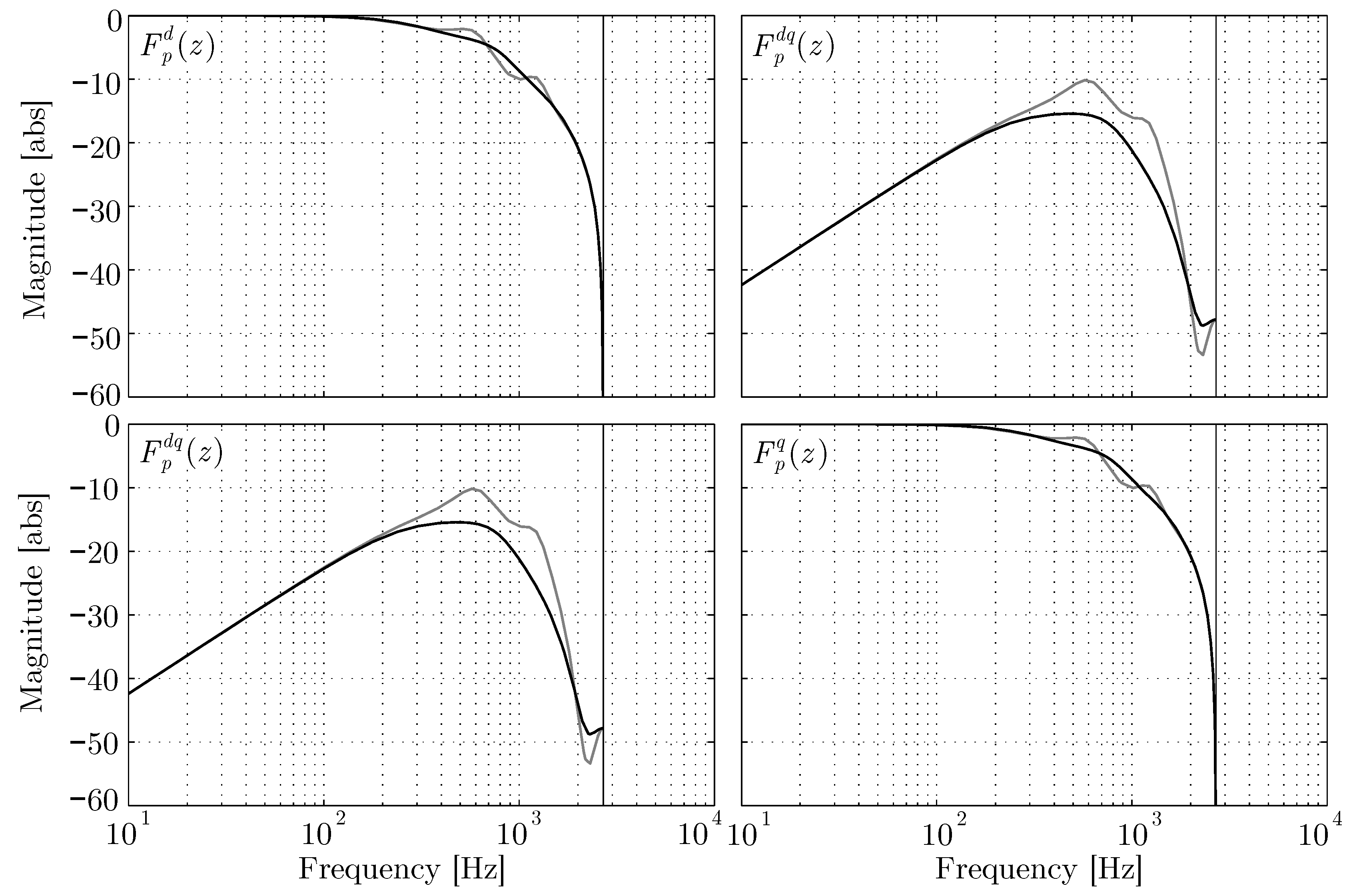
Figure 10 shows the frequency response magnitude of the transfer functions in Equation (25), with and without the state-variable predictions. For low frequencies both methods provide similar results, but near the resonance frequency the magnitude of the coupling terms were reduced by using predictions. This might be of interest when additional harmonic controllers are added to the control system.
5.3. Robustness Analysis
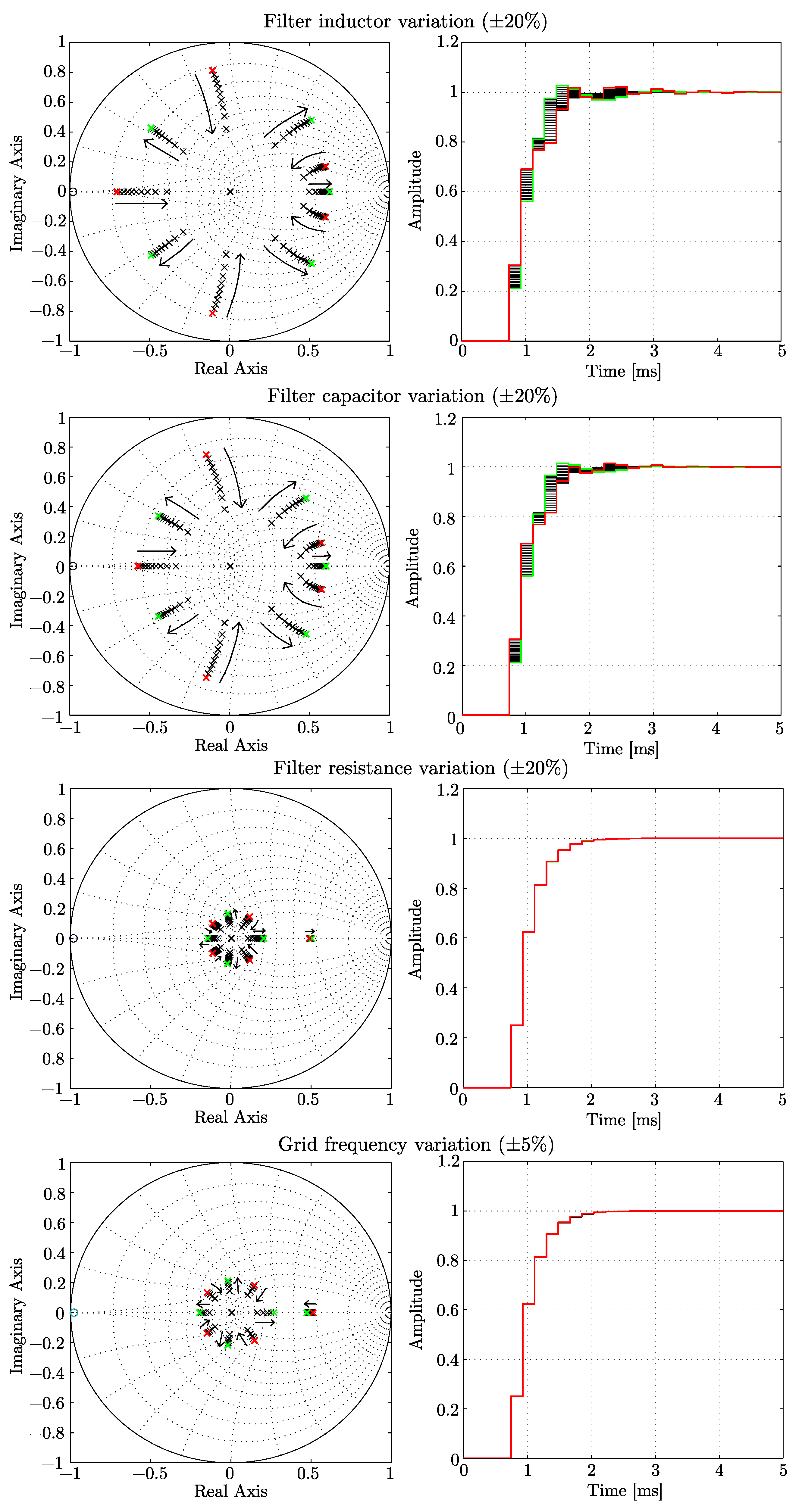
The control system robustness was tested against variations in the system parameters. Variations of % for the inductor, the capacitor, and the resistor of the connection filter were considered. Additionally, variations of % in the grid frequency were explored. Figure 12 shows the pole-zero map for the aforementioned cases. Variations in the filter inductor () and the filter capacitor () had a similar effect. In both cases, the resonance was less damped and the high-frequency poles approached the unit circle. This effect was more evident for the lowest values of and (in red). For variations in the filter resistor and in the grid frequency, the transient performance was almost unaffected, and only the high-frequency poles varied slightly. The controllability of the system was checked for all the possible cases, and the system was controllable (see Section 3.1 for more details).
5.4. Performance of the State-Feedback Controller
Voltage-Sag Compensation
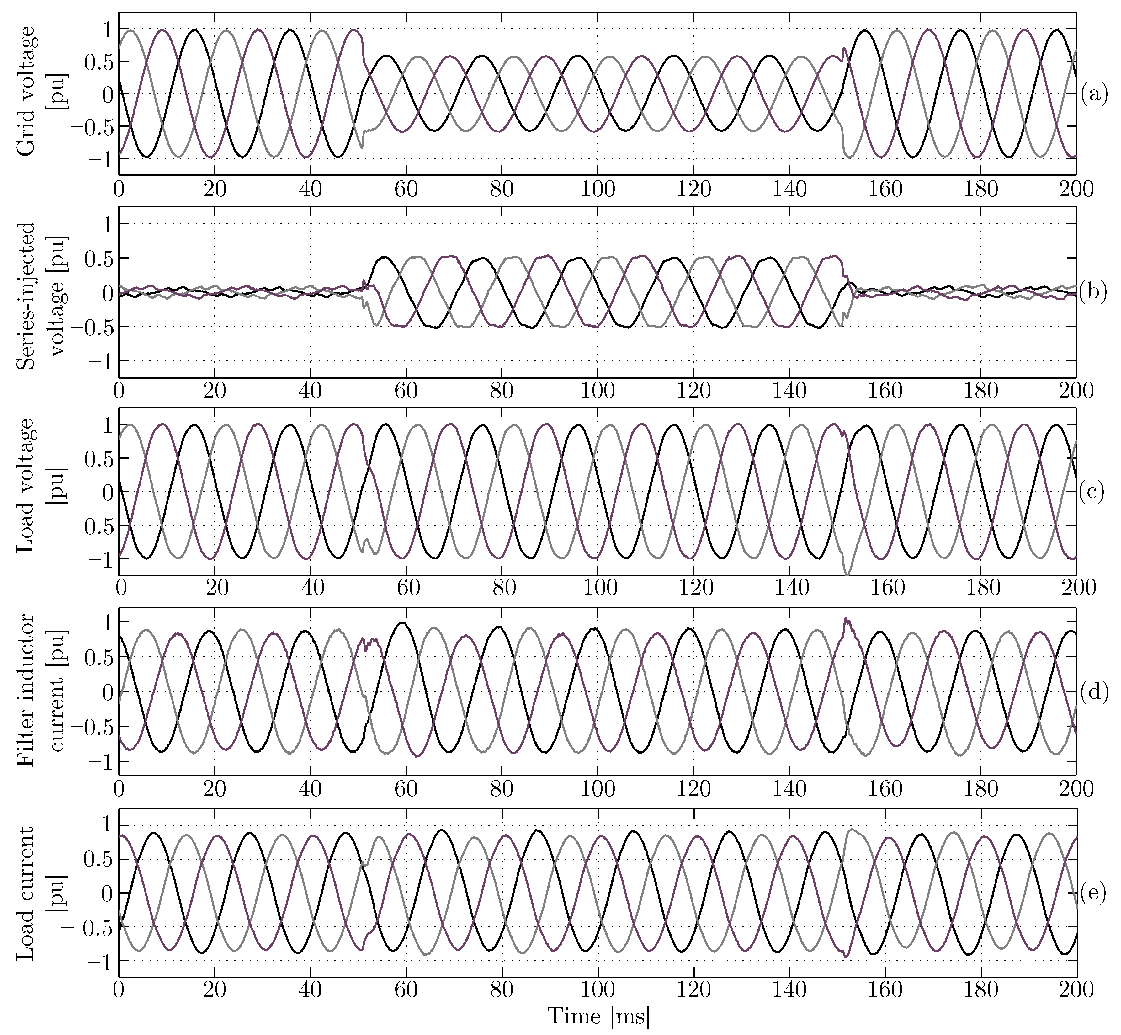
To start with, the DVR was tested under a three-phase voltage sag of 60% retained voltage. Figure 13 shows the experimental waveforms obtained for (a) the grid voltage, (b) the series-injected voltage, (c) the load voltage, (d) the current through the filter inductor, and (g) the load current. The series-injected voltage contains harmonic components due to the PWM process and the non-linearities of the coupling transformer. Therefore, the grid voltage Total Harmonic Distortion (THD) is 0.3% and the load voltage THD is 1.4%. At ms, a sag takes place and the DVR rapidly restores the load voltage. The filter inductor current had a small DC component during the transient, which decays slowly. This DC component is due to the transient of the load inductor flux (see Figure 7). When the sag ends, the DVR rapidly acts and the load voltage remains unaffected.
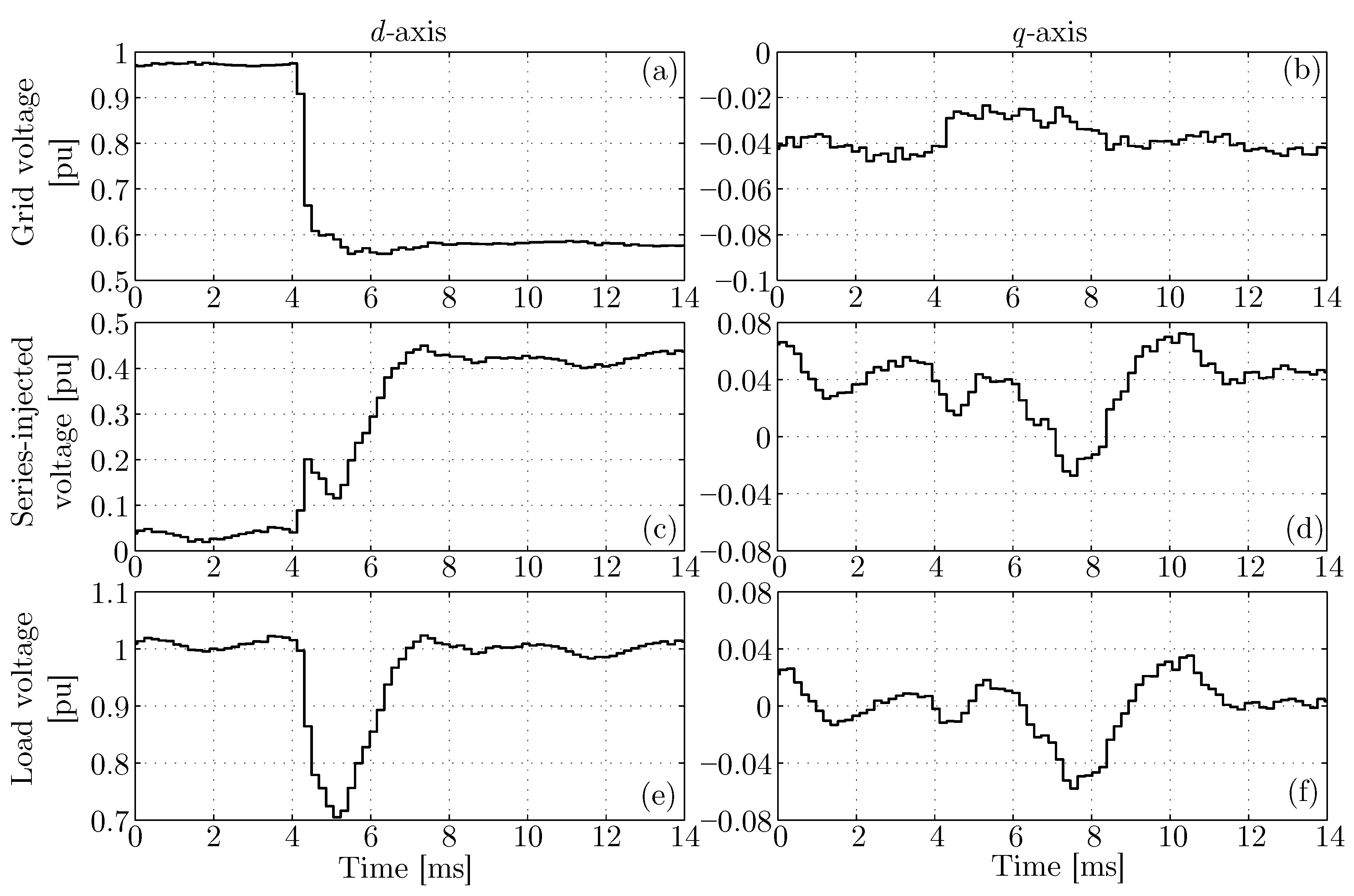
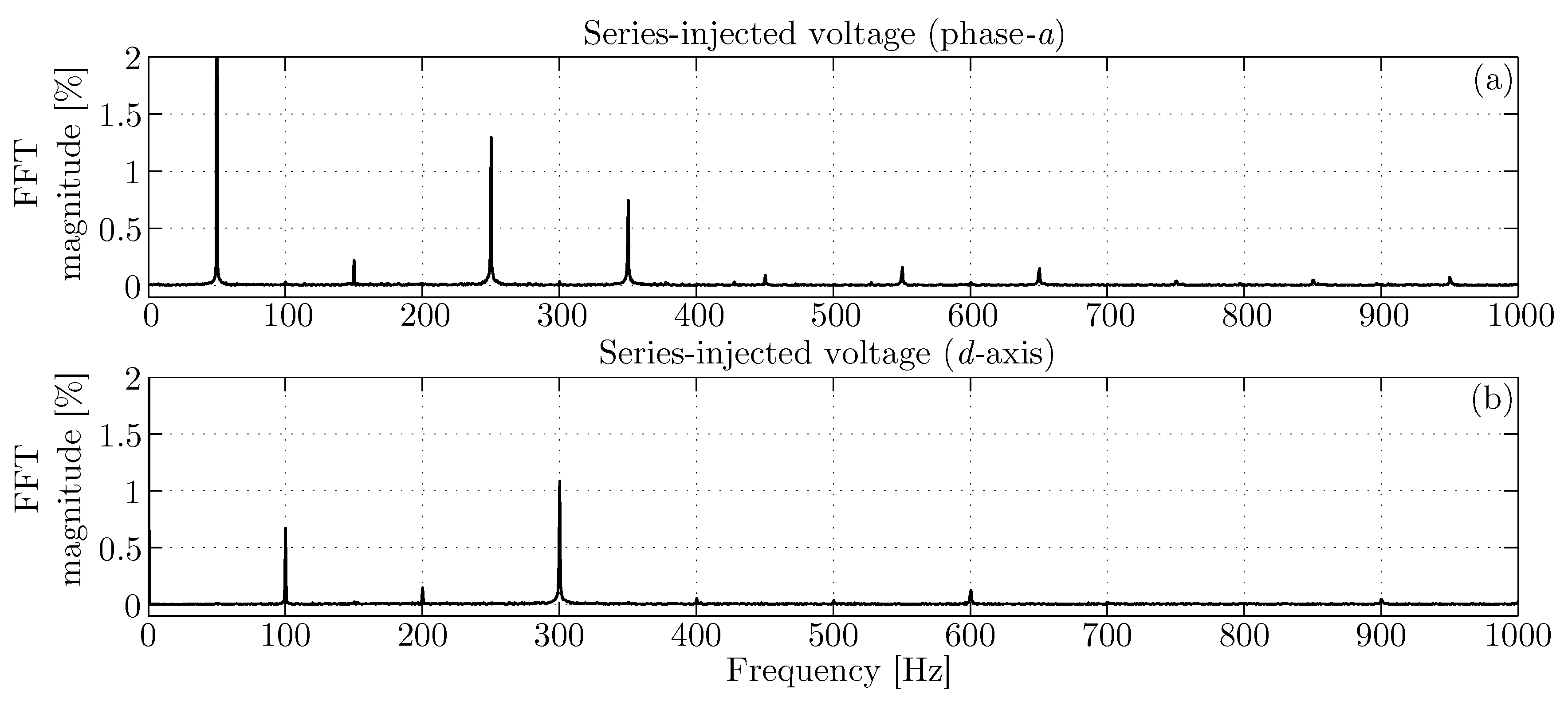
Figure 14 shows a detail of -components of (a and b) the grid voltage, (c and d) the series-injected voltage, and (e and f) the load voltage for the voltage sag in Figure 13. Before the sag, the d-axis component of the grid voltage is close to 1 pu because the PLL is forcing the SRF to rotate synchronously with the d-axis of the grid voltage. When the sag takes place, at ms of the time window shown, the DVR injects the required voltage, and, in less than 3 ms, the load voltage is restored. There is an oscillation with a period close to 3 ms in every picture in Figure 14 (e.g., Figure 14c), which corresponds to harmonics generated by the DVR. Figure 15 shows the results of a Fast Fourier Transform (FFT) applied to the load voltage over 75 cycles (1.5 s). The most important harmonics are 5th (negative sequence) and 7th (positive sequence) ( in three-phase variables and in ), which are likely generated by the coupling transformer. The component of frequency 100 Hz in corresponds to the negative-sequence component in three-phase variables.
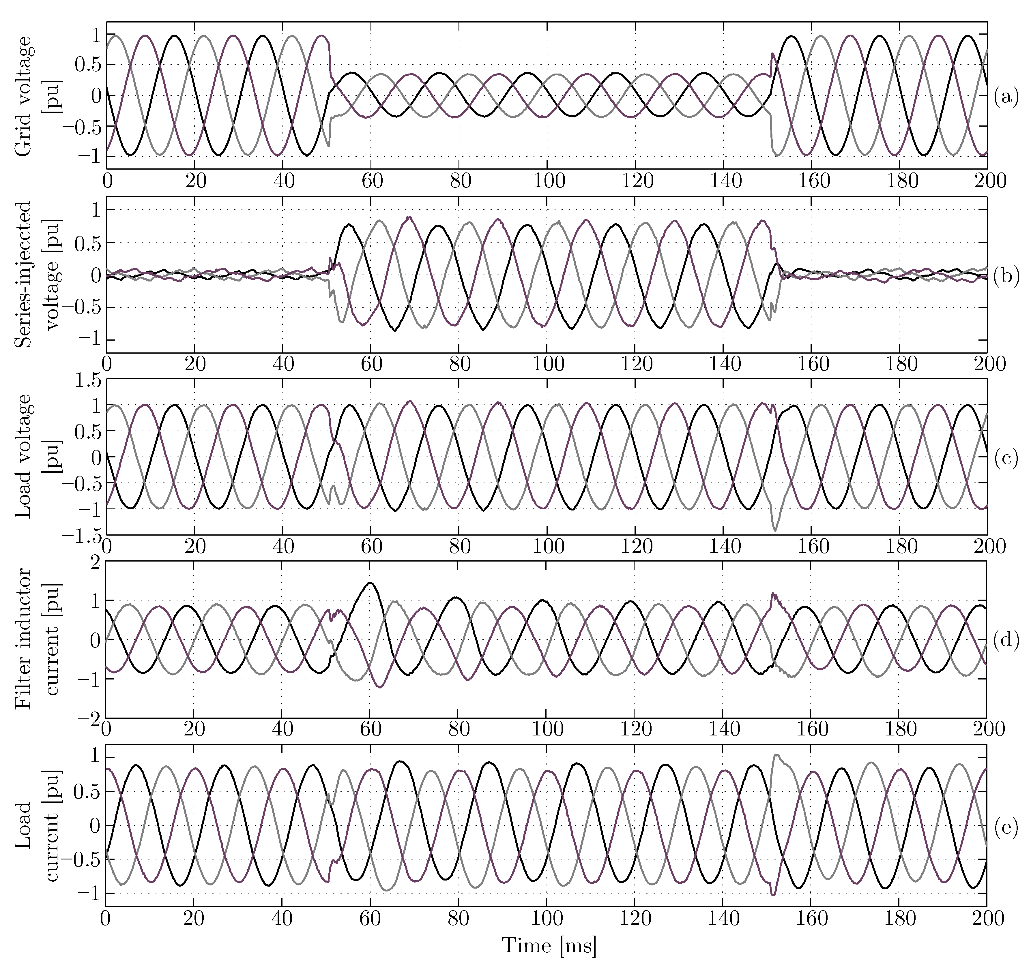
Figure 16 shows the DVR performance when compensating a deep voltage sag. Initially, the DVR was connected to the grid and all variables were in steady-state. At ms, a balanced voltage sag (35% retained voltage) took place and the DVR injected the series voltage needed to leave the load voltage undisturbed. One can see a large inrush current in Figure 16d when the compensation started because the coupling transformer saturated. The current through felt to its previous value after a few cycles, but the load current remained unbalanced because of the inductive load and the transient took several cycles to die out. This unbalance is due to the transient of the inductive load flux (see Figure 7).
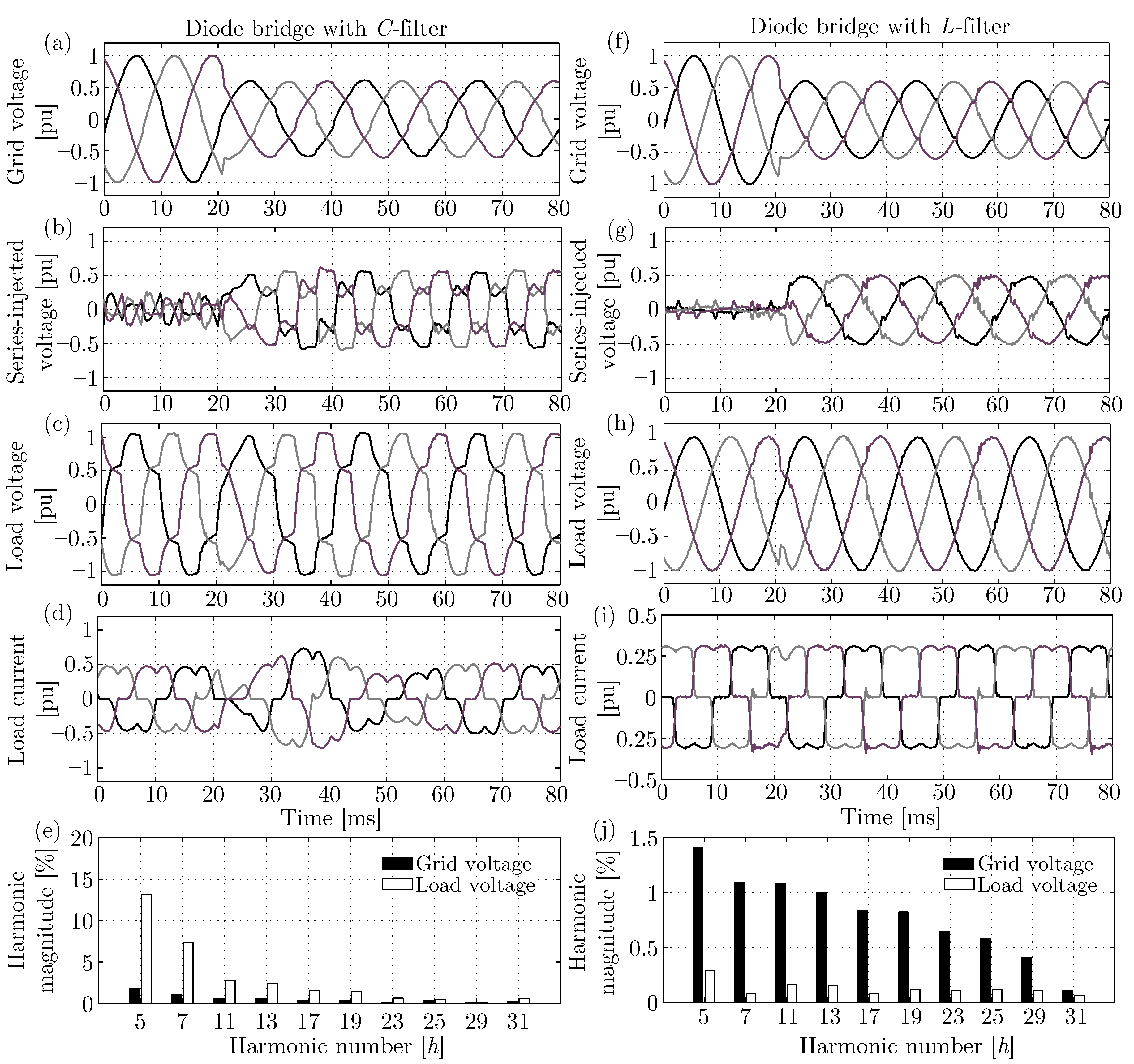
Figure 17 shows the transient performance of the DVR when the load was a diode bridge with (a) a C-filter (voltage-sourced load) and (b) an L-filter (current-sourced load). For the voltage-sourced load, the load voltage became highly distorted in steady state (THD was 24.6%). Figure 17e shows that the grid voltage quality deteriorated as well (THD was 4.6%). For the current-sourced load (Figure 17f–j) the load voltage THD was 3.2%, while the grid voltage THD was 3.8%. Therefore, the DVR worked better with current-sourced loads than with voltage-sourced loads.
5.5. Influence of the Load
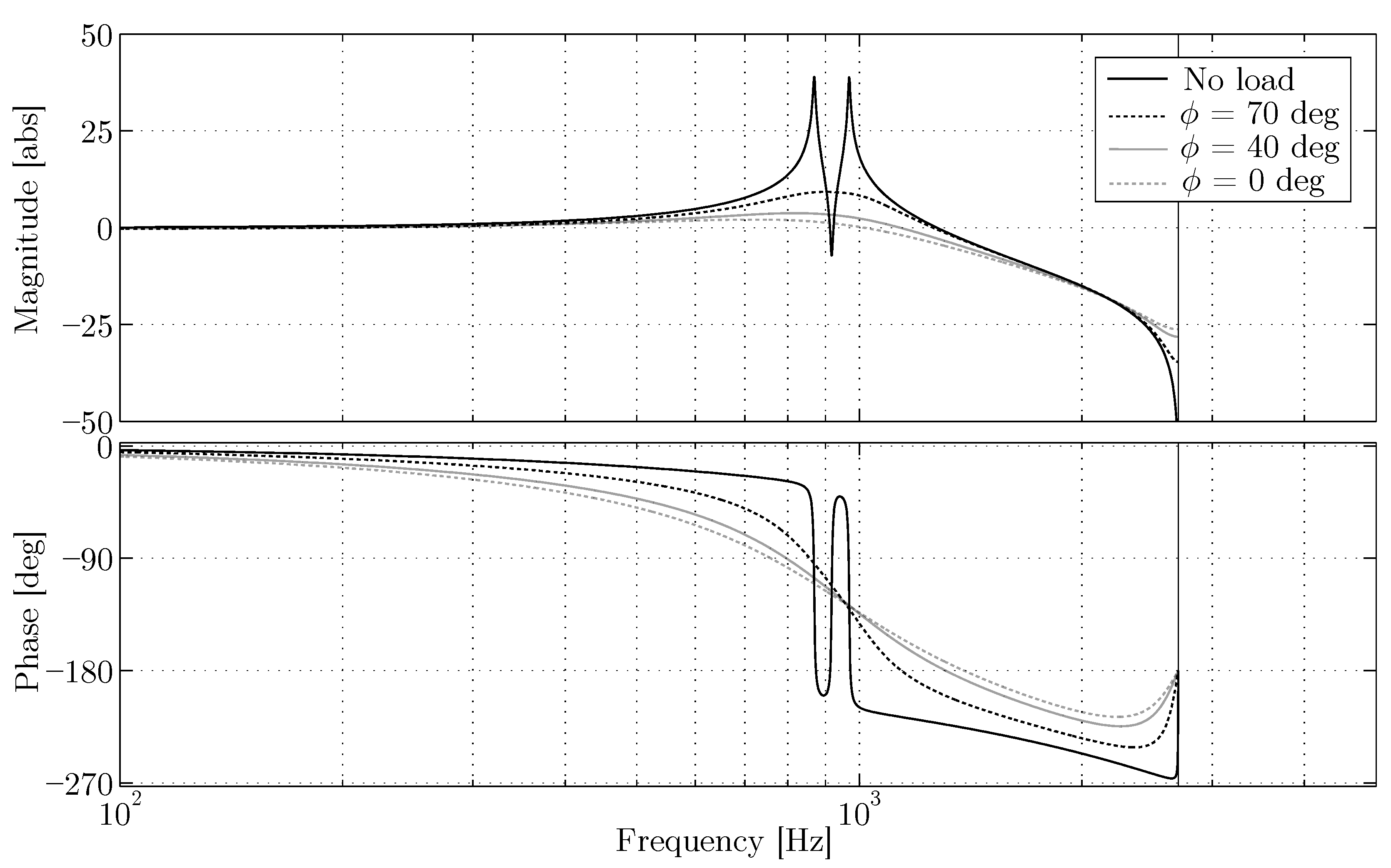
The DVR model obtained in Section 2 did not take into account the load. The load effects on the DVR performance can be reduced by adding a feed-forward of the load current, but this only compensates the low-frequency dynamics. The load can be modeled as an inductor () and a resistor () connected in parallel (see Figure 4):
Now, the load current is a state variable. Figure 18 shows the frequency response of the plant ( is the input and is the output) when adding a load of rated current with different power factors. The resonance is automatically damped, and the lower is (lower ), the lower the resonance peak is. Therefore, the DVR should work better when there is a load connected because the load clearly damps the resonance.
6. Alternatives for the Main Controller
The SF controller studied in Section 3 gives good results, but it has some considerable drawbacks. First of all, it is not easy to find a location for the closed-loop poles that results in reasonable stability margins, and, secondly, the design is not intuitive. In this section, two alternatives for the main controller are proposed and investigated, namely, a PID and a “cascade” controller. These are interesting alternatives because their design is more intuitive and they can be retuned in real time.
6.1. PID Controller
The set of decoupling equations suggested in Section 2 can accommodate several controller alternatives. In this section, the following continuous-time PID controller has been used:
which can be discretized by using the backward-Euler method [50], for example. This controller can be designed in continuous time by using frequency-response techniques [46]. However, the validity of the design has to be investigated after the discretization with the open- and closed-loop transfer functions. The model needed to design the controller can be obtained by converting the decoupled state-variable representation in Equation (15) into a transfer function [51]. The incremental controller approach can also be used to implement this controller, as suggested in Section 3.2 for the SF controller.
6.2. Cascade Controller
A “cascade” controller consists of two nested control loops, as shown in Figure 19. For a DVR, the inner controller handles the current through , and it is called the “inner-current controller.” The outer controller handles the load voltage modifying the current reference (), and it is called the “outer-voltage controller.” A cascade (multi-loop) controller is proposed by Vilathgamuwa et al. [52] for a DVR. However, the controller is implemented in a static RF, so zero steady-state error is not ensured for the fundamental component. This problem was solved by Wang et al. [53] by using a cascade controller referred to an SRF. However, neither Vilathgamuwa et al. [52] nor Wang et al. [53] investigated a discrete-time implementation.
The advantages of a cascade controller can be easily understood by using a single-phase continuous-time approach. Figure 19 shows the block diagram of the plant with the current and the voltage controllers. The plant seen by the outer-voltage controller can be obtained from Figure 19:
where is called virtual resistance. Clearly, the higher the value of () is, the better damped becomes, so can be easily designed. Once has been set, the voltage controller can be designed as a typical PID controller, where the open-loop transfer function is computed as follows:
where is shown in Figure 19. The proposed method simplifies the design of the inner controller, but the implementation must be investigated. Figure 20a shows the pole-zero diagram of modifying the value of , while Figure 20b shows the pole-zero diagram of (discrete-time equivalent of taking into account the ZOH and the calculus delay and anti-aliasing filters). In Figure 20b, the discrete-time poles have been moved to the continuous-time plane to simplify the comparison. It can be seen that, even if the closed-loop poles become stable, they move to the right-hand side of the complex plain when increases. Therefore, the filter resonance cannot be damped due to the delays present.
7. Main Controller Trade-offs
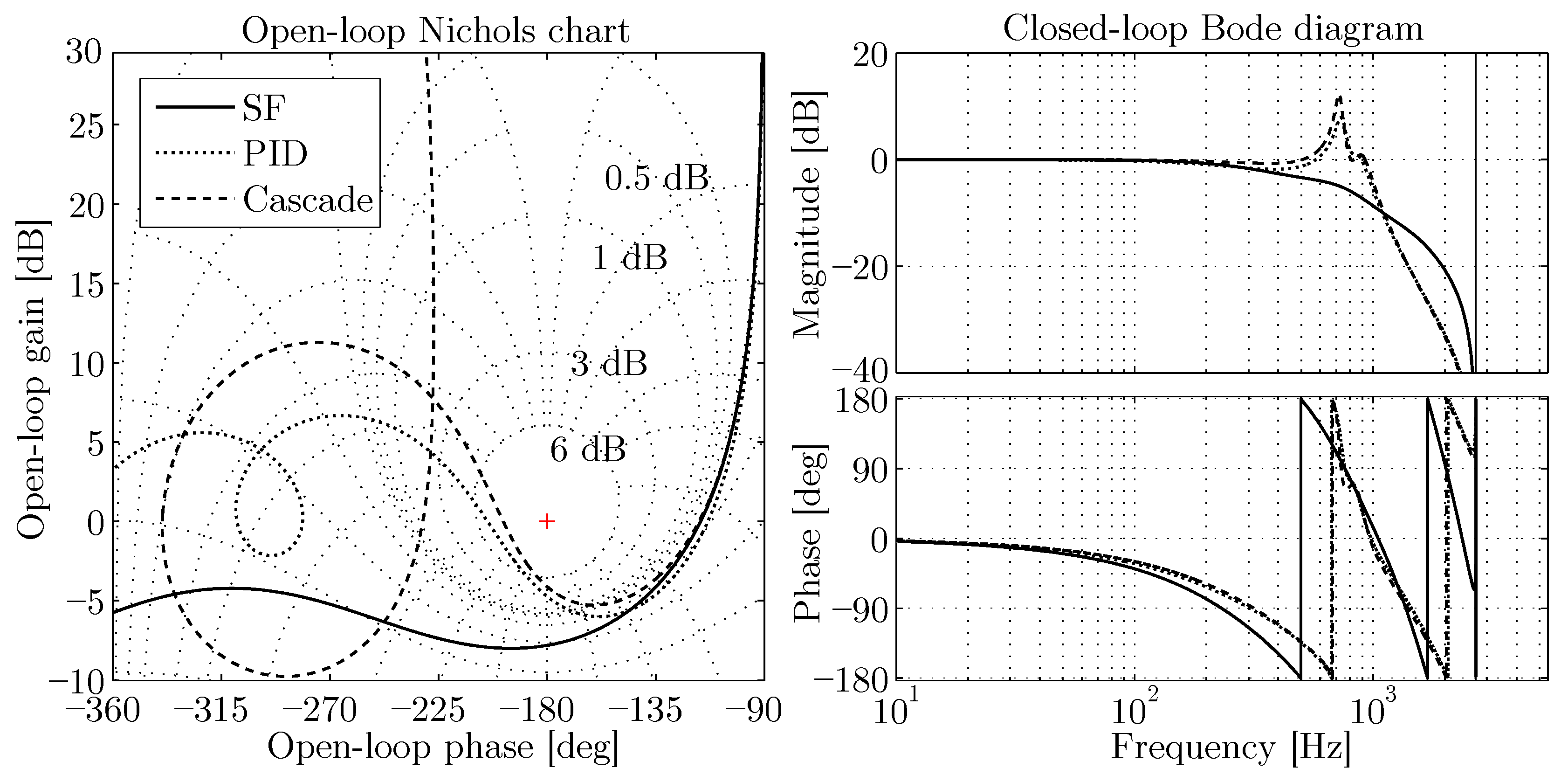
Figure 21 (left) shows the Nichols chart of (open-loop transfer function) for the SF, the PID, and the cascade controllers. All of them were designed to achieve the same phase margin of 60 deg (first crossing of 0 dB). It was assumed that the coupling effects between axes was negligible, so closed-loop stability was assessed by using Single-Input-Single-Output (SISO)s open-loop-based stability margins. The open-loop magnitude greatly increased at high frequency for the PID and the cascade controllers, suggesting that the resonance was not properly damped. In fact, Figure 21 (right) shows that the SF behaved better than the rest of the alternatives.
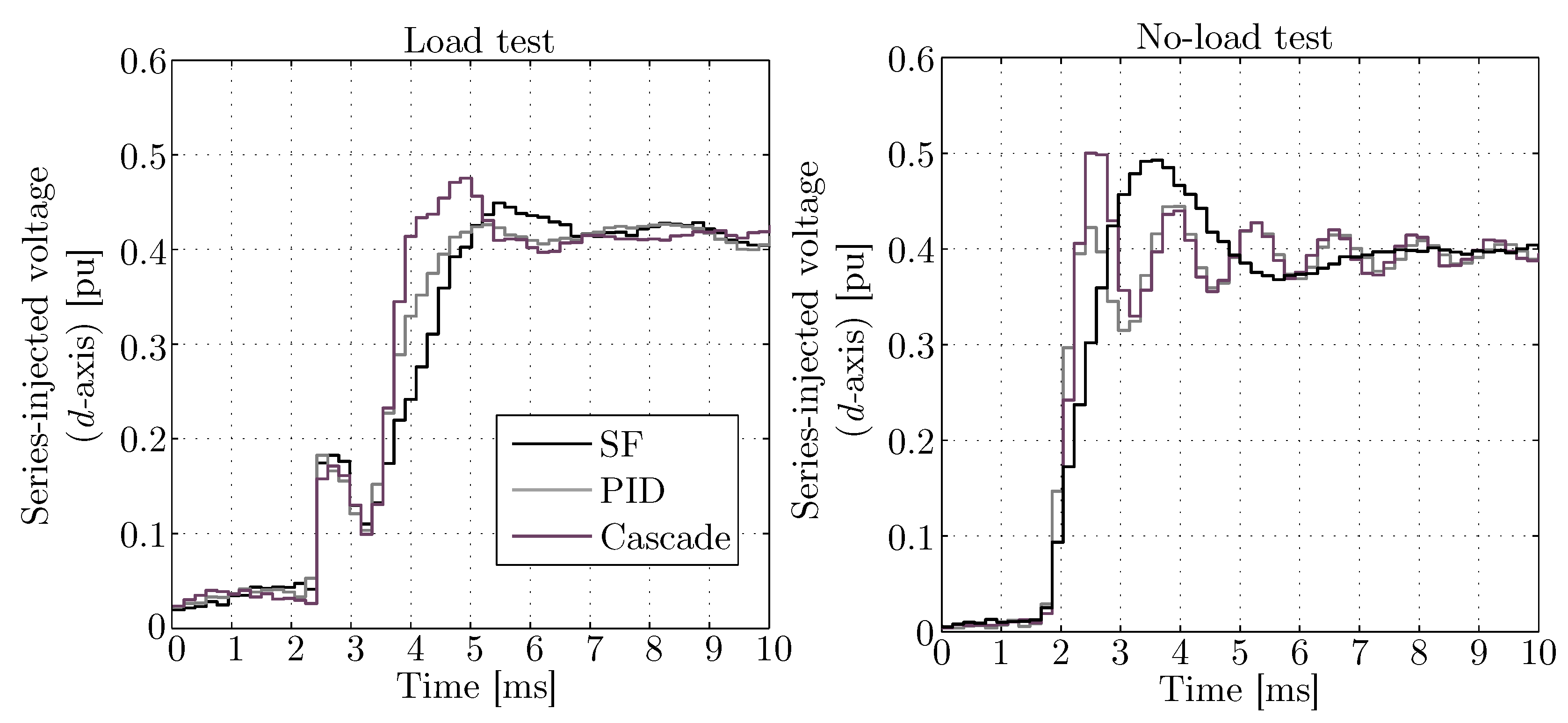
Figure 22 shows the transient of the DVR compensating a 60% retained-voltage sag when (left) there was a load connected downstream the DVR (230 V, 3.7 kW, and 2 kvar) and (right) there was no load. All the alternatives worked properly when a load was connected, but only the SF controller damped the resonance when there was no load (notice the oscillations with the PID and the Cascade controller).
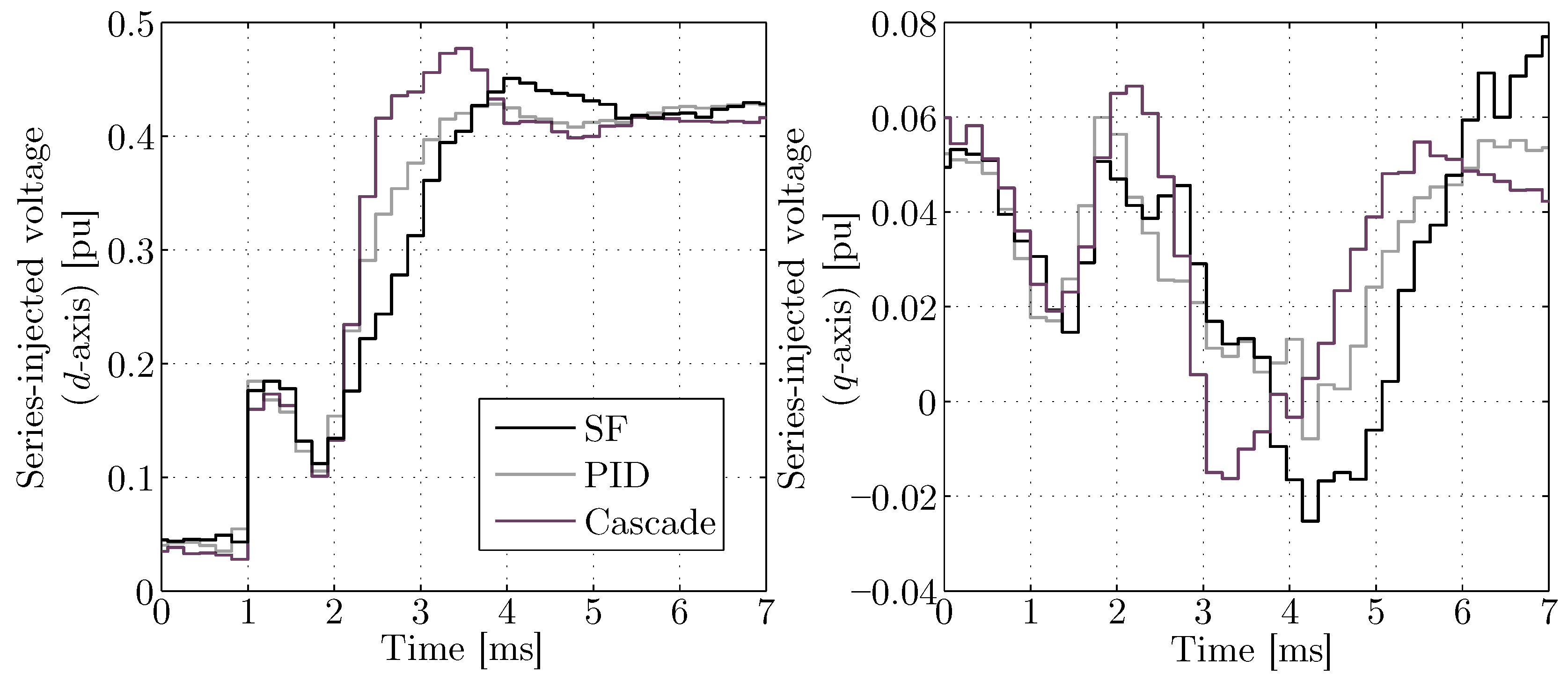
Figure 23 shows experimental results obtained when the DVR compensated a voltage sag of 60% retained voltage when there was a load connected (230 V, 3.7 kW, and 2 kvar). All the alternatives provided a fast transient response with reduced coupling effects and the cascade controller was the fastest one.
8. Conclusions
In this paper, the application of an SF controller for a DVR was presented. The DVR was modeled carefully and the state-space equations were discretized. An accurate method to decouple the dq-axis dynamics was developed and the controller was implemented in its incremental form. The proposed decoupling method minimized the coupling effects between the -axis dynamics. The design of the SF controller was carefully analyzed, including the effect of the load connected downstream the DVR. Two alternatives for placing the closed-loop poles were studied. It was found that both alternatives lead to similar results, although the LQR gave more robust controllers. Closed-loop system robustness was studied for variations in the filter parameters and in the grid frequency. It was found that the filter inductor and the filter capacitor had a more relevant impact, while the resistor and the frequency could be neglected. The DVR was tested protecting linear and non-linear loads. For current-source non-linear loads, the power quality of the output voltage deteriorated slightly. However, for voltage-source loads, the quality of the load voltage was poor. Two alternatives were compared with the SF controller: a PID and a cascade controller. The SF controller was less intuitive, but its design was straightforward. The PID and the cascade controllers exhibit accurate performance; however, when there was no load connected downstream the DVR, only the SF controller was able to properly damp the LC filter resonance. Control alternatives like hysteresis controllers can be found in the literature [23,24], and a comparative analysis with this alternative is of interest for further research. All the control system developments were validated in a 5 kVA prototype of a DVR, with accurate results.
Author Contributions
Formal analysis, J.R.-P., A.G.-C. and A.R.-C.; Investigation, J.R.-P.; Methodology, J.L.Z.-M.; Project administration, A.G.-C. and J.L.Z.-M.; Supervision, A.G.-C.; Validation, A.R.-C.; Writing—original draft, J.R.-P.; Writing—review & editing, A.G.-C. and J.L.Z.-M.
Funding
This research was funded by the Spanish Government’s grant number ENE2011-28527-c04-01.
Conflicts of Interest
The authors declare no conflict of interest.
References
- Bollen, M. Voltage sags: Effects, mitigation and prediction. Power Eng. J. 1996, 10, 129–135. [Google Scholar] [CrossRef]
- Carle, R. UPS applications: A mill perspective. IEEE Ind. Appl. Mag. 1995, 1, 12–17. [Google Scholar] [CrossRef]
- Roldán-Pérez, J.; García-Cerrada, A.; Ochoa-Giménez, M.; Zamora-Macho, J.L. On the Power Flow Limits and Control in Series-Connected Custom Power Devices. IEEE Trans. Power Electron. 2016, 31, 7328–7338. [Google Scholar] [CrossRef]
- Gyugyi, L.; Schauder, C.D.; Edwards, C.W.; Sarkozi, M. Apparatus and Method for Dynamic Voltage Restoration of Utility Distribution Networks. U.S. Patent 5,329,222, 12 July 1994. [Google Scholar]
- Antchev, M.; Petkova, M.; Gourgoulitsov, V.; Antchev, H. Investigation of Unified Voltage Conditioner (UVC). J. Power Electron. 2012, 12, 357–367. [Google Scholar] [CrossRef]
- Nielsen, J.G. Design and Control of a Dynamic Voltage Restorer. Ph.D. Thesis, Aalborg University, Aalborg, Denmark, 2002. [Google Scholar]
- Roldán-Pérez, J.; Zamora-Macho, J.L.; Ochoa-Giménez, M.; García-Cerrada, A. A steady-state harmonic controller for a series compensator with uncertain load dynamics. Electric Power Syst. Res. 2017, 150, 152–161. [Google Scholar] [CrossRef]
- Jimichi, T.; Fujita, H.; Akagi, H. An Approach to Eliminating DC Magnetic Flux From the Series Transformer of a Dynamic Voltage Restorer. IEEE Trans. Ind. Appl. 2008, 44, 809–816. [Google Scholar] [CrossRef]
- Li, B.H.; Choi, S.; Vilathgamuwa, D. Design considerations on the line-side filter used in the dynamic voltage restorer. IEE Proc. Gener. Transm. Distrib. 2001, 148, 1–7. [Google Scholar] [CrossRef]
- Choi, S.; Li, B.; Vilathgamuwa, D. Design and analysis of the inverter-side filter used in the dynamic voltage restorer. IEEE Trans. Power Deliv. 2002, 17, 857–864. [Google Scholar] [CrossRef]
- Goharrizi, A.Y.; Hossein, S.H.; Sabahi, M.; Charehpetian, G.B. Three-phase HFL-DVR with independently controlled phases. IEEE Trans. Power Electron. 2012, 27, 1706–1718. [Google Scholar] [CrossRef]
- Roncero-Sánchez, P.; Acha, E. Dynamic Voltage Restorer Based on Flying Capacitor Multilevel Converters Operated by Repetitive Control. IEEE Trans. Power Deliv. 2009, 24, 277–284. [Google Scholar] [CrossRef]
- Kim, H.; Sul, S.K. Compensation Voltage Control in Dynamic Voltage Restorers by Use of Feed Forward and State Feedback Scheme. IEEE Trans. Power Electron. 2005, 20, 1169–1177. [Google Scholar] [CrossRef]
- Ho, C.; Chung, H.; Au, K. Design and Implementation of a Fast Dynamic Control Scheme for Capacitor-Supported Dynamic Voltage Restorers. IEEE Trans. Power Electron. 2008, 23, 237–251. [Google Scholar] [CrossRef]
- Li, Y.W. Control and Resonance Damping of Voltage-Source and Current-Source Converters With Filters. IEEE Trans. Ind. Electron. 2009, 56, 1511–1521. [Google Scholar]
- Kanjiya, P.; Singh, B.; Chandra, A.; Al-Haddad, K. SRF theory revisited to Control Self-Supported Dynamic Voltage Restorer (DVR) for Unbalanced and Nonlinear Loads. IEEE Trans. Ind. Appl. 2013, 49, 2330–2340. [Google Scholar] [CrossRef]
- Li, Y.W.; Blaabjerg, F.; Vilathgamuwa, D.; Loh, P.C. Design and Comparison of High Performance Stationary-Frame Controllers for DVR Implementation. IEEE Trans. Power Electron. 2007, 22, 602–612. [Google Scholar] [CrossRef]
- Yazdani, A.; Iravani, R. Voltage-Sourced Converters in Power Systems; Wiley: Hooken, NJ, USA, 2010. [Google Scholar]
- Badrkhani Ajaei, F.; Afsharnia, S.; Kahrobaeian, A.; Farhangi, S. A Fast and Effective Control Scheme for the Dynamic Voltage Restorer. IEEE Trans. Power Deliv. 2011, 26, 2398–2406. [Google Scholar] [CrossRef]
- Roncero-Sánchez, P.; Acha, E.; Ortega-Calderón, J.; Feliu-Batlle, V.; García-Cerrada, A. Repetitive control for a dynamic voltage restorer for power-quality improvement. In Proceedings of the 13th European Conference on Power Electronics and Applications (EPE ’09), Barcelona, Spain, 8–10 September 2009; pp. 1–10. [Google Scholar]
- Hung, J. Feedback control with Posicast. IEEE Trans. Ind. Electron. 2003, 50, 94–99. [Google Scholar] [CrossRef]
- Mahdianpoor, F.; Hooshmand, R.; Ataei, M. A New Approach to Multifunctional Dynamic Voltage Restorer Implementation for Emergency Control in Distribution Systems. IEEE Trans. Power Deliv. 2011, 26, 882–890. [Google Scholar] [CrossRef]
- Petkova, M.; Antchev, M.; Gourgoulitsov, V. Investigation of single-phase inverter and single phase series active power filter with sliding mode control. Intech 2011. Available online: https://www.intechopen.com/books/sliding-mode-control/investigation-of-single-phase-inverter-and-single-phase-series-active-power-filter-with-sliding-mode (accessed on 1 June 2018). [CrossRef]
- Antchev, M.; Petkova, M.; Gurgulitsov, V. Sliding mode control of a single phase series active power filter. In Proceedings of the IEEE Conference EUROCON, Warsaw, Poland, 9–12 September 2007; pp. 1344–1349. [Google Scholar]
- Antchev, M.; Petkova, M.; Antchev, H.; Gourgoulitsov, V.; Valtchev, S. Study of Single-Phase Series Active Power Filter with Hysteresis Control. J. Energy Power Eng. 2012, 10, 1634–1641. [Google Scholar]
- Sasitharan, S.; Mishra, M. Constant switching frequency band controller for dynamic voltage restorer. IET Power Electron. 2010, 3, 657–667. [Google Scholar] [CrossRef]
- Jowder, F. Design and analysis of dynamic voltage restorer for deep voltage sag and harmonic compensation. IET Gener. Transm. Distrib. 2009, 3, 547–560. [Google Scholar] [CrossRef]
- Teke, A.; Bayindir, K.; Tumay, M. Fast sag/swell detection method for fuzzy logic controlled dynamic voltage restorer. IET Gener. Transm. Distrib. 2010, 4, 1–12. [Google Scholar] [CrossRef]
- Jurado, F. Neural network control for dynamic voltage restorer. IEEE Trans. Ind. Electron. 2004, 51, 727–729. [Google Scholar] [CrossRef]
- Elnady, A.; Salama, M. Mitigation of voltage disturbances using adaptive perceptron-based control algorithm. IEEE Trans. Power Deliv. 2005, 20, 309–318. [Google Scholar] [CrossRef]
- Saleh, S.; Moloney, C.; Azizur Rahman, M. Implementation of a Dynamic Voltage Restorer System Based on Discrete Wavelet Transforms. IEEE Trans. Power Deliv. 2008, 23, 2366–2375. [Google Scholar] [CrossRef]
- Loh, P.C.; Holmes, D.G. Analysis of multiloop control strategies for LC/CL/LCL-filtered voltage-source and current-source inverters. IEEE Trans. Ind. Appl. 2005, 41, 644–654. [Google Scholar] [CrossRef]
- Blasko, V.; Kaura, V. A novel control to actively damp resonance in input LC filter of a three-phase voltage source converter. IEEE Trans. Ind. Appl. 1997, 33, 542–550. [Google Scholar] [CrossRef]
- Cheng, P.T.; Chen, J.M.; Ni, C.L. Design of a State-Feedback Controller for Series Voltage-Sag Compensators. IEEE Trans. Ind. Appl. 2009, 45, 260–267. [Google Scholar] [CrossRef]
- Hasanzadeh, A.; Edrington, C.; Maghsoudlou, B.; Fleming, F.; Mokhtari, H. Multi-loop linear resonant voltage source inverter controller design for distorted loads using the linear quadratic regulator method. IET Power Electron. 2012, 5, 841–851. [Google Scholar] [CrossRef]
- Huerta, F.; Pizarro, D.; Cobreces, S.; Rodriguez, F.J.; Giron, C.; Rodriguez, A. LQG Servo Controller for the Current Control of LCL Grid-Connected Voltage-Source Converters. IEEE Trans. Ind. Electron. 2012, 59, 4272–4284. [Google Scholar] [CrossRef]
- Ochoa-Giménez, M.; García-Cerrada, A.; Zamora-Macho, J.L. Comprehensive control for unified power quality conditioners. J. Mod. Power Syst. Clean Energy 2017, 5, 609–619. [Google Scholar] [CrossRef] [Green Version]
- Roldán-Pérez, J.; García-Cerrada, A.; Zamora-Macho, J.L.; Roncero-Sánchez, P.; Acha, E. Troubleshooting a digital repetitive controller for a versatile dynamic voltage restorer. Int. J. Electr. Power Energy Syst. 2014, 57, 105–115. [Google Scholar] [CrossRef]
- Krause, P.C.; Wasynczuk, O.; Sudhoff, S.D. Analysis of Electric Machinery and Drive Systems, 2nd ed.; Wiley-IEEE Press: Piscataway, NJ, USA, 2002. [Google Scholar]
- Pinzón-Ardila, O. Selective Harmonic Compensation by Using Active Power Filters. Ph.D. Thesis, Comillas Pontifical University, Madrid, Spain, 2007. [Google Scholar]
- García-González, P. Modelling, Control and Application of “FACTS” based on Voltage Source Converters (VSCs). Ph.D. Thesis, Universidad Pontificia Comillas, Madrid, Spain, 2009. [Google Scholar]
- Åström, K.J.; Wittenmark, B. Computer Controlled Systems; Prentice-Hall: Upper Saddle River, NJ, USA, 1984. [Google Scholar]
- García-Cerrada, A.; Pinzón-Ardila, O.; Feliu-Batlle, V.; Roncero-Sánchez, P.; García-González, P. Application of a Repetitive Controller for a Three-Phase Active Power Filter. IEEE Trans. Power Electron. 2007, 22, 237–246. [Google Scholar] [CrossRef]
- García-González, P.; García-Cerrada, A. Control system for a PWM-based STATCOM. IEEE Trans. Power Deliv. 2000, 15, 1252–1257. [Google Scholar] [CrossRef]
- Roldán-Pérez, J.; García-Cerrada, A.; Zamora-Macho, J.L.; Roncero-Sánchez, P.; Acha, E. Adaptive repetitive controller for a three-phase dynamic voltage restorer. In Proceedings of the 3rd IEEE International Conference on Power Engineering, Energy and Electrical Drives, Malaga, Spain, 11–13 May 2011. [Google Scholar]
- Kuo, B. Automatic Control System; Prentice-Hall International London: London, UK, 1962. [Google Scholar]
- Astrom, K.J.; Hagglund, T. PID Controllers: Theory, Design, and Tuning, 2nd ed.; International Society for Measurement and Con: Research Triangle Park, NC, USA, 1995. [Google Scholar]
- Skogestad, S.; Postlethwaite, I. Multivariable Feedback Control: Analysis and Design; John Wiley & Sons: Chichester, UK, 2005. [Google Scholar]
- Rodríguez-Cabero, A.; Sánchez, F.H.; Prodanovic, M. A unified control of back-to-back converter. In Proceedings of the 2016 IEEE Energy Conversion Congress and Exposition (ECCE), Milwaukee, WI, USA, 18–22 September 2016; pp. 1–8. [Google Scholar]
- Kuo, B. Digital Control Systems; Oxford University Press: New York, NY, USA, 1992. [Google Scholar]
- Friedland, B. Control System Design: An Introduction to State-Space Methods; McGraw-Hill Series in Electrical Engineering: Control Theory; McGraw-Hill: London, UK, 1986. [Google Scholar]
- Vilathgamuwa, M.; Perera, A.; Choi, S. Performance improvement of the dynamic voltage restorer with closed-loop load voltage and current-mode control. IEEE Trans. Power Electron. 2002, 17, 824–834. [Google Scholar] [CrossRef]
- Wang, B.; Venkataramanan, G.; Illindala, M. Operation and control of a dynamic voltage restorer using transformer coupled H-bridge converters. IEEE Trans. Power Electron. 2006, 21, 1053–1061. [Google Scholar] [CrossRef]
Figure 1.
Most relevant dynamic voltage restorer (DVR) control strategies: (a) open-loop control, (b) single-loop control, (c) multi-loop control, and (d) single-loop control with current feed-forward.
Figure 1.
Most relevant dynamic voltage restorer (DVR) control strategies: (a) open-loop control, (b) single-loop control, (c) multi-loop control, and (d) single-loop control with current feed-forward.

Figure 2.
Single-phase schematics of the proposed set-up and the controller of a DVR.

Figure 3.
Overview of the control strategy for a DVR. Two independent controllers are used.

Figure 4.
Single-phase electrical model for the DVR.

Figure 5.
Incremental form of the state-feedback (SF) controller. stands for the incremental operator and stands for the accumulation operator (the state-variable predictions are not shown for simplicity).
Figure 5.
Incremental form of the state-feedback (SF) controller. stands for the incremental operator and stands for the accumulation operator (the state-variable predictions are not shown for simplicity).

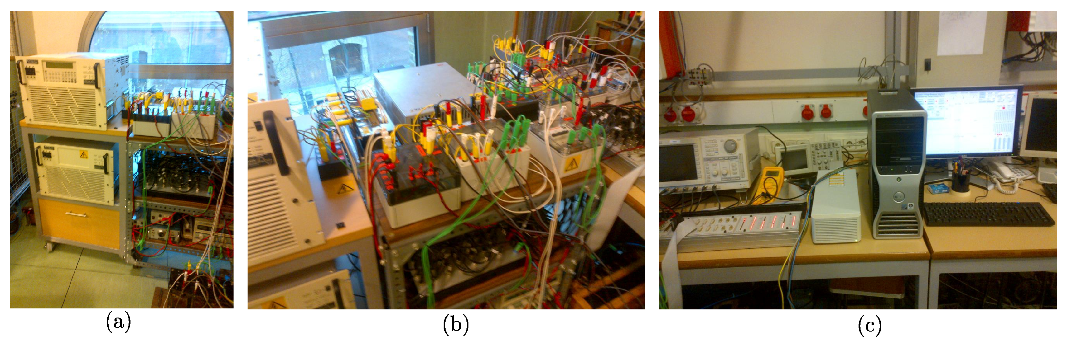
Figure 6.
Photographs of the experimental platform. (a) Programmable voltage source, (b) (left) DVR and connection elements and (right) loads, and (c) dSpace platform, oscilloscopes, and external computer.
Figure 6.
Photographs of the experimental platform. (a) Programmable voltage source, (b) (left) DVR and connection elements and (right) loads, and (c) dSpace platform, oscilloscopes, and external computer.

Figure 7.
Schematics of the prototype. The power can be taken from an auxiliary electrical network, the grid-side of the DVR, or the load-side of the DVR.
Figure 7.
Schematics of the prototype. The power can be taken from an auxiliary electrical network, the grid-side of the DVR, or the load-side of the DVR.

Figure 8.
Pole placement alternatives. (left) Step response with (blue) manual and (red) linear quadratic regulator (LQR) gain selection. Closed-loop system poles and zeros when the filter inductor varies from % to % for (center) LQR and (right) manual pole placement.
Figure 8.
Pole placement alternatives. (left) Step response with (blue) manual and (red) linear quadratic regulator (LQR) gain selection. Closed-loop system poles and zeros when the filter inductor varies from % to % for (center) LQR and (right) manual pole placement.

Figure 9.
(left) Pole-zero diagram of (grey) the uncompensated plant in Equation (15) ( is the input and is the output) and (black) the compensated plant, . (right) Bode diagram of (grey) the uncompensated plant and (black) the compensated plant.
Figure 9.
(left) Pole-zero diagram of (grey) the uncompensated plant in Equation (15) ( is the input and is the output) and (black) the compensated plant, . (right) Bode diagram of (grey) the uncompensated plant and (black) the compensated plant.

Figure 10.
Bode plot of , , , and , (black) with predictions and (grey) without predictions.

Figure 11.
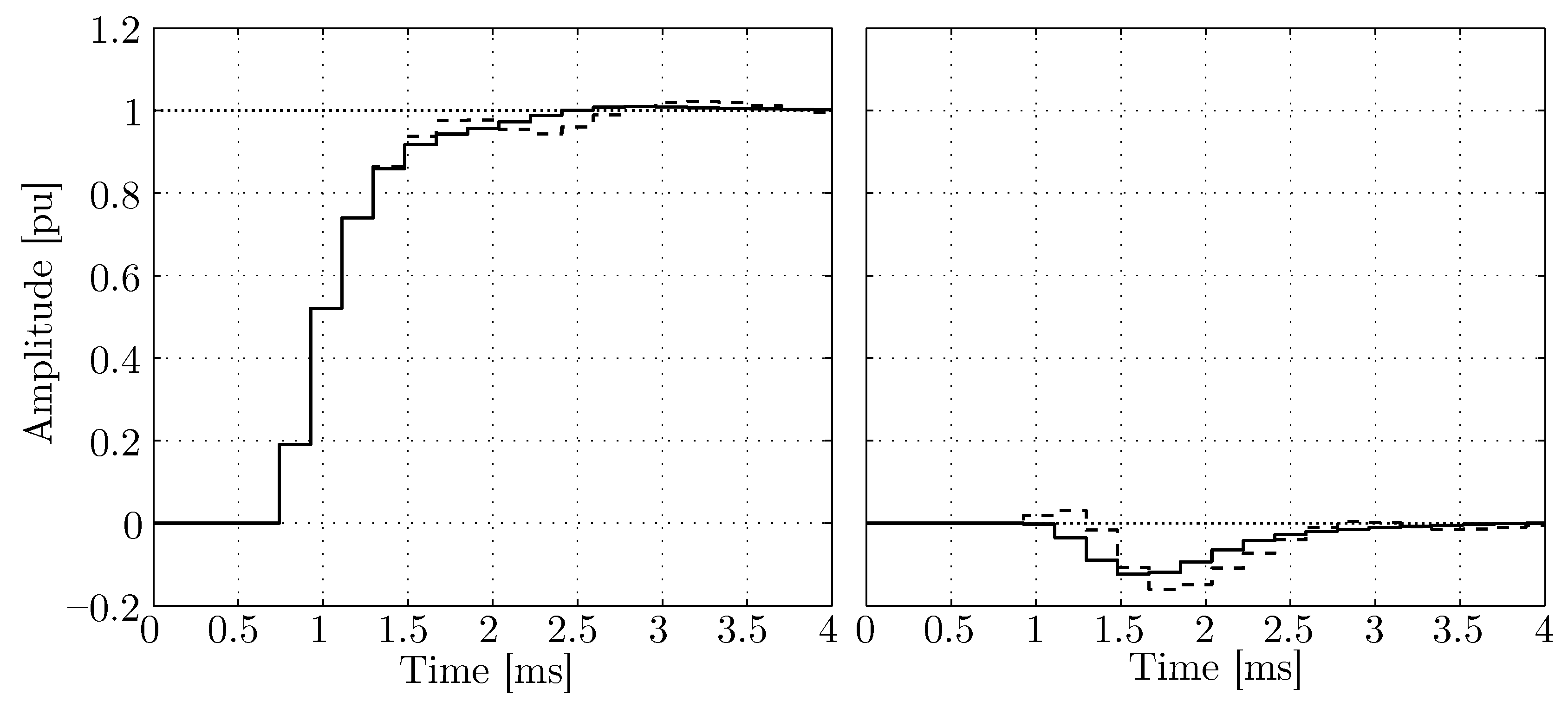
Simulation. Step response of (left) and (right) (solid) using predictions and (dashed) without predictions.
Figure 11.
Simulation. Step response of (left) and (right) (solid) using predictions and (dashed) without predictions.

Figure 12.
Pole-zero analysis of the closed-loop control system when the value of the hardware elements is modified. From top to bottom, filter inductor, filter capacitor, filter resistance, and grid frequency. (red) Initial value of (green) final value. Arrows indicate the increasing direction.
Figure 12.
Pole-zero analysis of the closed-loop control system when the value of the hardware elements is modified. From top to bottom, filter inductor, filter capacitor, filter resistance, and grid frequency. (red) Initial value of (green) final value. Arrows indicate the increasing direction.

Figure 13.
Experimental results. Mitigation of a sag (60% retained voltage) with the SF controller. (a) Grid voltage, (b) series-injected voltage, (c) load voltage, (d) filter inductor current, and (e) load current.
Figure 13.
Experimental results. Mitigation of a sag (60% retained voltage) with the SF controller. (a) Grid voltage, (b) series-injected voltage, (c) load voltage, (d) filter inductor current, and (e) load current.

Figure 14.
Experimental results. Mitigation of a 60% retained-voltage sag with an SF controller using in-phase compensation (signals referred to a synchronous reference frame (SRF)). (a) d- and (b) q-axis grid voltage, (c) d- and (d) q-axis series-injected voltage, and (e) d- and (f) q-axis load voltage.

Figure 15.
Experimental results. FFT modulus of the series-injected voltage: (a) phase-a and (b) d-axis.
Figure 15.
Experimental results. FFT modulus of the series-injected voltage: (a) phase-a and (b) d-axis.

Figure 16.
Experimental results. Voltage sag compensation (35% retained voltage) with the SF controller. (a) Grid voltage, (b) series-injected voltage, (c) load voltage, (d) filter inductor current, and (e) load current.
Figure 16.
Experimental results. Voltage sag compensation (35% retained voltage) with the SF controller. (a) Grid voltage, (b) series-injected voltage, (c) load voltage, (d) filter inductor current, and (e) load current.

Figure 17.
Experimental results. Mitigation of a 60% retained voltage sag when the load is a diode bridge with (a–e) a C-filter and (f–j) an L-filter. (a,f) Grid voltage, (b,g) series-injected voltage, (c,h) load voltage, (d–i) load current, and (e–j) harmonic content of the (black) grid and (white) load voltages.

Figure 18.
Frequency response of the plant when using a parallel load, for different values of ( is the angle of the load impedance). In all cases (except in the one called “no load”) the load consumes the nominal current at the rated voltage.
Figure 18.
Frequency response of the plant when using a parallel load, for different values of ( is the angle of the load impedance). In all cases (except in the one called “no load”) the load consumes the nominal current at the rated voltage.

Figure 19.
Simplified block diagram of a DVR with a cascade controller.

Figure 20.
Root locus of (a) and (b) , shifting the value of . The arrows indicate the zero-pole movement when increases.
Figure 20.
Root locus of (a) and (b) , shifting the value of . The arrows indicate the zero-pole movement when increases.

Figure 21.
(left) Open-loop Nichols chart and (right) closed-loop Bode diagram for (solid) the SF, (dotted) the PID, and (dashed) the cascade controllers.
Figure 21.
(left) Open-loop Nichols chart and (right) closed-loop Bode diagram for (solid) the SF, (dotted) the PID, and (dashed) the cascade controllers.

Figure 22.
Experimental results. d-axis component of the series-injected voltage for the PID, the cascade, and the SF controllers (left) with the load and (right) without the load.
Figure 22.
Experimental results. d-axis component of the series-injected voltage for the PID, the cascade, and the SF controllers (left) with the load and (right) without the load.

Figure 23.
Experimental results. -axis components of the series-injected voltage for the PID, the cascade, and the SF controllers when the load is connected. (left) d- and (right) q-axis component.
Figure 23.
Experimental results. -axis components of the series-injected voltage for the PID, the cascade, and the SF controllers when the load is connected. (left) d- and (right) q-axis component.


Table 1.
Base values used in this paper.
| Variable Name | Base Name | VSC Side | Grid Side |
|---|---|---|---|
| Apparent power (VA) | |||
| Phase voltage (V) | |||
| Current (A) | |||
| Impedance () | |||
| Frequency (rad/s) |
© 2018 by the authors. Licensee MDPI, Basel, Switzerland. This article is an open access article distributed under the terms and conditions of the Creative Commons Attribution (CC BY) license (http://creativecommons.org/licenses/by/4.0/).
Share and Cite
MDPI and ACS Style
Roldán-Pérez, J.; García-Cerrada, A.; Rodríguez-Cabero, A.; Zamora-Macho, J.L. Comprehensive Design and Analysis of a State-Feedback Controller for a Dynamic Voltage Restorer. Energies 2018, 11, 1972. https://doi.org/10.3390/en11081972
AMA Style
Roldán-Pérez J, García-Cerrada A, Rodríguez-Cabero A, Zamora-Macho JL. Comprehensive Design and Analysis of a State-Feedback Controller for a Dynamic Voltage Restorer. Energies. 2018; 11(8):1972. https://doi.org/10.3390/en11081972
Chicago/Turabian StyleRoldán-Pérez, Javier, Aurelio García-Cerrada, Alberto Rodríguez-Cabero, and Juan Luis Zamora-Macho. 2018. "Comprehensive Design and Analysis of a State-Feedback Controller for a Dynamic Voltage Restorer" Energies 11, no. 8: 1972. https://doi.org/10.3390/en11081972
Note that from the first issue of 2016, this journal uses article numbers instead of page numbers. See further details here.