Fast Transient Modulation for a Step Load Change in a Dual-Active-Bridge Converter with Extended-Phase-Shift Control


Faculty of Information Technology, Macau University of Science and Technology, Avenida Wai Long, Taipa, Macau SAR 999078, China
*
Author to whom correspondence should be addressed.
Energies 2018, 11(6), 1569; https://doi.org/10.3390/en11061569
Submission received: 8 May 2018
/
Revised: 11 June 2018
/
Accepted: 12 June 2018
/
Published: 14 June 2018
(This article belongs to the Section F: Electrical Engineering)
Abstract
:The manipulation of the bidirectional power in a dual-active-bridge converter relies on the adjustment of several phase-shift angles. Improper implementation of those adjustments during the transient process of a step load change may induce transient DC bias current in the transformer and accompanied high peak current, which may result in excess loss and safety issues potentially. The paper proposes a load transient modulation to execute the adjustments of the two phase-shift angles for extended-phase-shift (EPS) control in a predictive manner. An unknown phase-shift is introduced to the gating signals of one bridge arm, and the gating signals of other bridge arms would be modified accordingly to realize the required adjustment of the two phase-shift angles together. With the proper selection of the introduced phase-shift, the power adjustment can be done in less than one high-frequency cycle without resulting in DC bias and overshoot current. Although there are four different operation modes existing in EPS, a universal solution of the unknown phase-shift can be obtained for all possible power transition cases between different modes. Validation of the proposed method is performed by means of both simulation and experimental tests.
1. Introduction
Isolated bidirectional DC/DC converters (IBDCs) are the key components in energy storage systems in applications of renewable generation and electrical transportation [1,2,3,4,5,6,7,8,9,10,11,12,13,14,15,16,17,18]. Generally, it is used as an interface between two voltage sources for bidirectional power exchange. As a typical voltage-fed IBDC, the dual-active-bridge (DAB) DC/DC converter has been discussed continuously and extensively in the literature for more than two decades. Featured with high power density, high efficiency and a wide range of zero-voltage switching (ZVS) operations, initially, it was proposed to be controlled by an outer phase-shift, named phase-shifted modulation (PSM) or single phase-shift (SPS) [9,10,11]. However, there are two apparent drawbacks associated with SPS control: limited ZVS operation range with non-unity converter gain and high circulating current at partial load. Different modulation techniques are then proposed to either extend the ZVS range or alleviate the circulating current, which include extended phase-shift (EPS) [6,12,13,14,15,16], dual-phase-shift (DPS) [17,18,19,20,21] and triple-phase-shift (TPS) [22,23,24]. Generally, those advanced control strategies introduce one or two controllable inner phase-shifts, so that the power becomes a function of up to three variables. Additionally, there are some research works focusing on the modeling and closed-loop control of a DAB converter. Comparatively, there are only a few works reported concerning the transient performance of a DAB converter, especially the step-change of phase-shift angles [25,26,27,28,29,30,31]. When a step load change is requested in a DAB converter, one or more phase-shift angles are to be adjusted accordingly to let the converter move from one steady state to another. Those adjustments are realized by manipulating the gating signals of those active switches. It can be proven easily that unplanned and arbitrary implementation of those adjustments may induce transient DC bias current in the transformer and accompanied high peak current, which may result in excess loss and safety issues potentially. Using a series DC-blocking capacitor is a simple and effective way to eliminate DC bias in the high-frequency (HF) transformer current resulting from static inconsistencies of gating signals and switch parameters. However, the stored energy in the DC-blocking capacitor due to the step change of phase-shift angles could result in current oscillation and extend the settling period. Furthermore, the extra capacitor increases the cost and the volume of the converter. The instantaneous current control in a DAB converter [25] provides another effective solution at the cost of complicated control design and circuitry. In [26], the required increment of the outer phase-shift was distributed unevenly to the two bridges according to an optimized ratio so that no DC bias current would arise during the transition process. Following that principle, a transient strategy is developed in [27] that can be applied in EPS. However, no investigations of its capability to perform a transition in negative power modes and perform power direction reversion are revealed. Furthermore, when the converter gain approaches unity, the given solution with a near-zero denominator would result in an extra-large phase-shift, which will make the inductor current become discontinuous. A similar solution was given for a single-phase DAB under SPS control in [28] by changing the gating signals of two arms in one bridge twice continuously, which could also be applied to reverse the power flow instantly. However, it may induce a peak current under some specific conditions. In [29], the voltage-time balance during the process of changing load was maintained by temporarily introducing two more phase-shifts, though the steady-state control was still SPS. Furthermore, the transient effect on the magnetizing inductance of the HF transformer was considered in this work. The work presented in [30] tried to use a similar principle for a three-phase DAB converter under TPS control to eliminate the transient DC bias. However, the solution was given with an assumption of a fixed outer phase-shift angle. In order to avoid the saturation problem, an excellent, but complex method called “magnetic ear” was proposed in [31], which requires an auxiliary core and extra circuit to compensate for the DC bias. Conclusively, until now, most of the reported solutions were limited to SPS control. As mentioned early, many advanced control techniques have adopted two or more phase-shifts for power manipulation with more different operation modes. Consequently, there will be more different transition cases, and the complexity level to adjust more phase-shift angles together increases, as well. Therefore, it will be meaningful to search for a new transient modulation for those multi-phase-shift control schemes. In this work, a predictive load transient modulation for EPS control will be proposed to execute the adjustment of gating signals during the load-changing process. It will be proven to be applicable for any of the possible cases of transition between the different steady-state operation modes. The associated simple calculation and easy implementation make it an economic and effective solution.
The rest of the paper is organized as follows. Section 2 describes the principle of EPS control and its associated distinctive operation modes. One transition case is used as an example to illustrate the problems if direct transient modulation is used. The proposed load transient modulation is presented in Section 3 for fast and smooth transition, which are explained in detail in three different categories. In Section 4, the transition cases using the proposed transient modulation are verified by a series of experimental tests. Finally, conclusions are drawn in Section 5.
2. Load Transient Problem under EPS Control
The circuit schematic of a DAB converter with its steady-state equivalent circuit is shown in Figure 1. Two active full-bridges are connected via an HF transformer and a power inductor . The transformer magnetizing inductance is assumed to be infinite, and the transformer leakage inductance can be included as part of . The power can be exchanged between two DC voltage sources and . The series resistance is an equivalent parasitic resistance including the total winding resistance and the on-state resistances of switches.
The two phase-shifts adopted in EPS include one inner phase-shift and one outer phase-shift . According to [14,15], the inner phase-shift should be used on the high-voltage side to achieve better performance. In this work, it is assumed that is higher than . Therefore, the inner phase-shift is defined as the phase delay from the turn-on moment of to that of , which ranges from 0– regardless of the power direction. The outer phase-shift is defined as the phase delay from the turn-on moment of to those of , , which can be either positive or negative. Based on the relationship among , and average power , there are four different steady-state operation modes: A, A, B, B. The superscript indicates the power direction, with “+” for the power flowing from to and “−” for the power flowing from to . In Figure 2, the steady-state waveforms of the four modes are illustrated with the gating signals of all switches presented. It can be seen that those modes differ from each other in the power direction, the relationship of the two phase-shift angles and the shape of the inductor current. The range of phase-shift angles in each mode is illustrated in Figure 3. In each steady-state time interval, a general differential equation can be written by referring to the equivalent circuit in Figure 1:
Solving this first-order RLcircuit yields:
If the time constant is much larger than the duration of the time interval , Equation (2) can be approximated as:
which is widely used for steady-state analysis of DAB converters in the literature. Therefore, the instantaneous current values at the switching moments of all switches can be found as the functions of by solving Equation (3) in one HF period sequentially. Those currents are normalized by the base value and are concluded in Table 1. The converter voltage gain is defined as: .
When a step load change in a DAB converter happens, the two phase-shift angles are to be changed to accordingly. It is assumed that the values of will be determined by one preset control strategy for the purpose of some performance optimization. In the current work, the main focus is put on the effect of the implementation of those modifications of phase-shift angles on the transient performance in a DAB converter.
Since a DAB converter with EPS control has four different operation modes, the number of total transition cases is up to . In the later part, the notation {x, y} will be used to denote a transition from mode x to mode y, where x or y can be any of the four different modes. From the definition of , it can be seen that those two phase-shifts are relative positions referring to the turn-on moments of . Therefore, if are supposed to be adjusted, the simple and direct way is to change the related delay of the turn-on moments of and , referring to that of . One example of such a direct transient modulation (DTM) applied to the transition {A, A} is shown in Figure 4. It is assumed that the gating signals of switch arm (, ) will not be changed. Consequently, the turn-on moment of and the turn-on moment of , are delayed from the previous position by and , respectively. Thus, the adjustment of the two phase-shift angles is finished in . The values of the new steady-state tank current can be obtained as:
Compared with the content of Table 1, those values are different from the theoretical values expected at in Mode A. The valley current is the same as before, while the peak current is higher than the theoretical new peak current. While bringing up some extra conduction loss, this unexpected peak current or overshoot current may be out of the safe operation area (SOA) of the switches. Furthermore, the average current after the transition process is not zero:
The theoretical reason can be viewed from the waveform of shown in Figure 4a, as well. It is seen that the voltage-time product of the inductor in the initial steady state is . Due to the implementation of the adjustment of gating signals, the voltage-time product then becomes . Although the voltage-time balance is still kept after , there is a net increment from to :
which indicates the consequence of Equation (8). The simulation of such a transition using DTM for is presented in Figure 4b with the waveforms of , and . In the left part with a large time scale, the overshoot peak current after the transient modulation can be easily identified from the envelope of the inductor current. The vertical asymmetry of the current waveform reveals the existence of a DC bias current. The details of the transition process are demonstrated in the right part, which matches the theoretical prediction given in Figure 4a. In an actual DAB converter, the overshoot current and non-zero DC bias current will decay gradually due to the non-zero parasitic resistance . In Figure 5, simulation plots of transient responses under DTM with three different are presented. It can be seen that the larger is, the faster the DC bias current will decay. However, a larger is not preferable since it results in more copper loss. Theoretically, the negative effects due to direct changes of two phase-shift angles exist in other cases of transition, as well. Therefore, the adjustments to the two phase-shift angles should be executed in a proper manner so that the total transient duration is significantly reduced and has no dependance on . Meanwhile, the temporal overshoot current and DC bias current are expected to be zero.
3. Fast Transient Modulation For EPS Control
In this section, a new control method during the step load changing procedure called fast transient modulation (FTM) is proposed for fast and smooth transition, which can be applied in any of the possible cases in EPS control. The basic principle of the proposed FTM is to select one movable reference, to which all phase-shift angles will be adjusted. The reference selected in this work is the falling edge of (i.e., the turn-off moment of ). Different from the situation in DTM, the reference will be moved by an undetermined angle during the transient process, whose value should be chosen properly so that the resultant instantaneous current right after the transient state matches the expected value in the new steady state. According to the type of destination steady state mode, all possible transition cases with EPS can be divided into three categories, each of which will be dealt with one by one.
3.1. Type I: Within One Mode
All transition cases, in which the initial mode and the final mode are the same, fall into this category. The transition {A, A} is used as an example to explain the application of FTM. The theoretical waveforms of the proposed FTM in the transition {A, A} are illustrated in Figure 6a. Compared with the DTM in Figure 4, a unknown phase-shift is cut off from the on-duration of S. Accordingly the turn-on moment of S and the turn-on moment of , will be delayed by and , respectively. Except for those changes, other switches maintain the original 50% duty cycle operation. Therefore, the required adjustments of are completed during . The durations of each interval in the process are , , . Although the whole transition process lasts until , it can be found that the durations of each interval after already match those of the new steady state. The instantaneous current at can be calculated as:
Assuming that the value of is selected properly so that the converter enters into the expected new steady state after , the new steady-state value located at can be predicted according to Table 1:
The two currents above are expected to be equal, which yields:
The validity of the FTM can be explained again using the voltage-time balance across the inductor. According to the plot of in Figure 6a, the voltage-time products of the transient state are found as:
Thus, the net changes of the voltage-time product during the transient interval of [ ] and [ ] are:
To keep the voltage-time balance without delay, it is expected that . Through calculation, the expression of can be obtained the same as Equation (12). By inserting Equation (12) into Equations (14) and (15), it is found that:
This relationship shows the principle behind FTM in that the total increment of the voltage-time product is executed in two equal steps, i.e., a certain amount of energy more than before is stored in the inductor in the first step (), and the same amount of energy more than the stored energy is then released in the second step ().
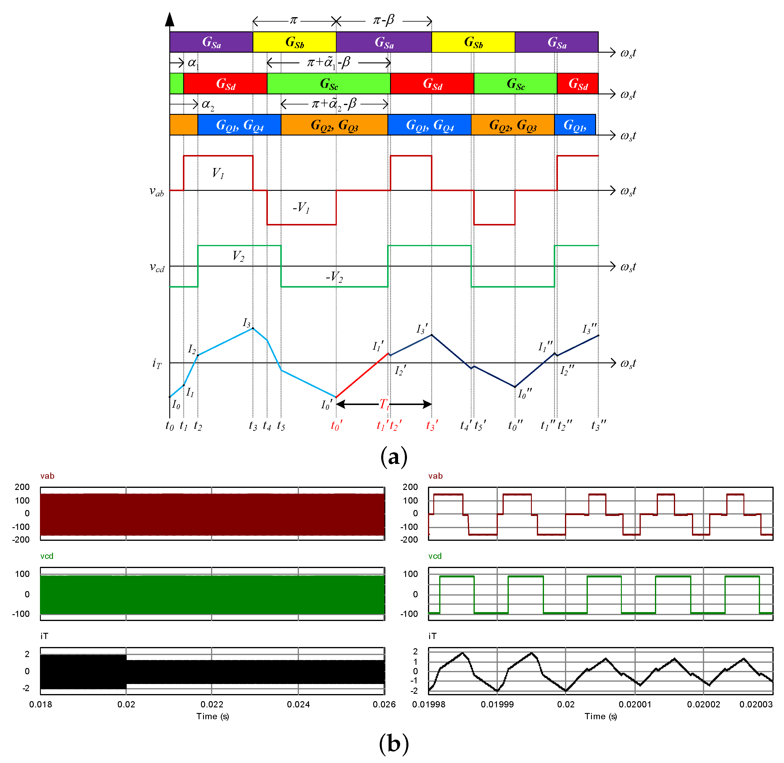
The simulated plots of such a transition case using FTM are presented in Figure 6b, which uses the same parameters as those in Figure 4b. With a time scale of 20 ms in the left part, there is no noticeable overshoot current in the envelope of the transformer current. The right part with a resolution of 10 s clearly matches the predicted waveforms in Figure 6a.
3.2. Type II: Between Two Modes with the Same Power Direction
A transition of Type II involves two different modes with the same power direction. Two examples for each power direction will be given to illustrate the transition process using FTM. The example for the positive power direction is the case of {A, B}. As presented in Figure 7a, the transition period starts at and ends at . The durations of three time intervals in the process are , , , respectively, which indicates that the new steady state can start from as early as . The instantaneous current at is given by:
It is supposed to be equal to the new steady-state value at , which can be predicted from Table 1:
By letting Equation (17) equal Equation (18), the obtained solution of is found to be the same as Equation (12). The validity of such an implementation can be proven by the simulated plots in Figure 7b with the almost instant step response of the tank current. It can be noticed that the rising edge of (from 0–) and that of swap positions during the transition period, which indicates the mode transition from A to B.
To give more evidence of this type, theoretical and simulated waveforms of {A, B} for negative power transfer are illustrated in Figure 8. It can be seen that the transient period includes four time intervals, which is different from the examples before. The durations of each intervals are , , , , respectively. The new steady state can be expected to start from . The instant current located at can be calculated as:
Since the final mode changes to B, is supposed to be the same as the new steady state current at the turn-on moment of . With the help of Table 1, is predicted as:
By equaling the two currents, the expression of for this transition can be obtained, which has the same result as Equation (12). Without noticeable overshoot and DC bias current in the transient process, the simulation proof shown in Figure 8b verified the effectiveness and correctness of FTM again. Furthermore, it can be observed that the polarity of outer phase-shift (the phase shift between the turn-on moment of and that of ) changes after the transition. It is seen that the Type II transition in negative power takes two more time intervals to complete the transient process. However, the expression of the key parameter still remains unchanged.
3.3. Type III: Between Two Modes with the Reverse Power Direction
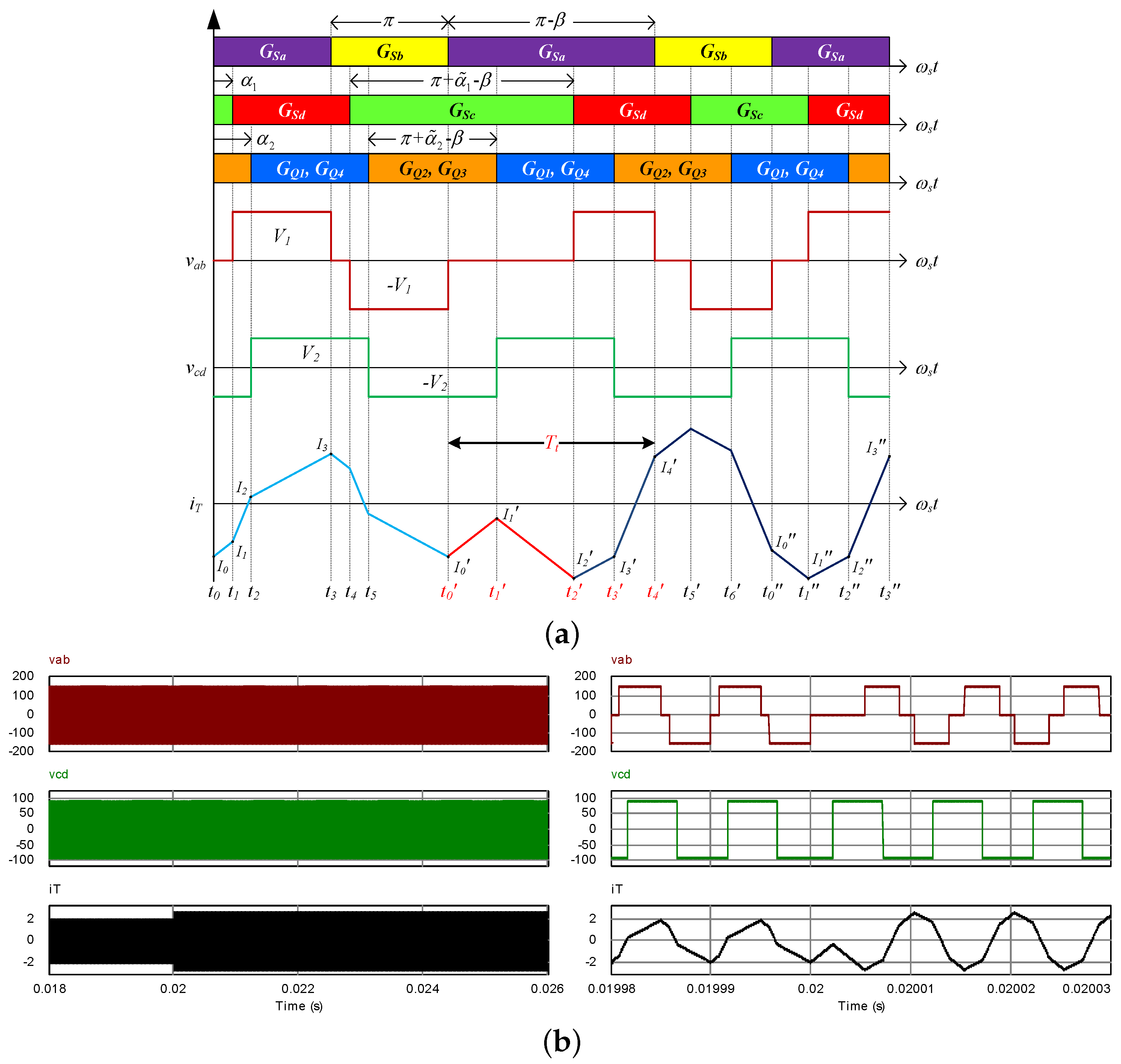
Generally, the transitions for reverse power tend to be more complicated. However, they can be realized similarly. For example, all reverse-power transitions can be accomplished in two steps: the power level in one direction can be adjusted to zero power in Step 1 and then changed from zero power to high power in the other direction in Step 2. Actually, the zero power under EPS control is the boundary between Mode B and Mode B, as indicated in Figure 3. Additionally, since there are no differences between Mode B and Mode B in terms of the expressions of instantaneous currents according to Table 1, the transition cases {A, B}, {A, B} would be the same as the previously discussed {A, B}, {A, B}, respectively. In the following discussion, the transition {A, A} is adopted as an example for direct transition from positive power to negative power. The ideal transition procedure using the proposed FTM is shown in Figure 9. The whole transition period starts from and ends at , which includes four time intervals. The durations of the four time intervals are , , and , respectively. Compared to the regular time intervals in Mode A, it can be seen that the new steady state is supposed to start from . The instantaneous current at is given as:
Again, this current is supposed to be equal to the new steady-state current , which is given by:
It can be found that the expressions in Equations (21) and (22) are the same as those in Equations (19) and (20) even though they have different meanings. Consequently, the value of can be solved by equalizing the two currents, which is the same as Equation (12) again. In Figure 9b, the simulation results of this case show the exact waveforms as the theoretical prediction.
Based on the discussion above, some features of the proposed FTM can be concluded as: (a) A phase-shift , which is dependent on the converter voltage gain, is applied on the gating signals of switch arm (, ). The gating signals of other arms will be adjusted accordingly to fulfill the increments , . (b) As for the effects on the two HF voltages, the rising edge (from 0–) and the falling edge (from –0) of and the rising edge of are shifted during the transition period . (c) The transient period always ends at the falling edge (from –0) of , while the sequence of the other two shifted edges may swap depending on the transition type. (d) The whole transition period has three or more time intervals depending on the transition types. However, the actual transient duration, which is between the initial and final steady state, is less than .
4. Experimental Verification
To verify the proposed FTM practically, a prototype of a DAB converter is built and tested in the lab. The voltage levels of two voltage sources are: = 150V; = 90V. The HF transformer is built using a ETD-49 ferrite core. The turns ratio is :1 = 10:10. Therefore, the converter voltage gain is . The measured magnetizing inductance and total leakage inductance are 390 H and 0.8 H, respectively. Including the leakage inductance of the transformer, the effective inductance of the power inductor is H. The switching frequency is kHz. The model of MOSFET switches on the high-voltage side is STP40NF20 with , and the model of MOSFET switches on the low-voltage side is IPP200N15N3 with . The key specifications of the experiment are concluded in Table 2, and a photo of the actual circuit setup is presented in Figure 10.
The layout for the implementation of the proposed FTM using a TI-F2835 DSP (Digital-Signal-Processor) development board is give in Figure 11. The flowchart of the program executed in the DSP is illustrated in Figure 12. The DSP program checks its input regularly for a new power command. Once a new power command of is confirmed, the power difference is evaluated. The actual power level P is calculated by sampling the DC voltage and current on one side. If is larger than a threshold value, the phase-shift selector will start to search for new of the target load level. As mentioned before, the strategy used in the phase-shift selector can be customized for the purpose of any performance requirement. In the experimental setup, a look-up table is just used as an example, of which the values of phase-shifts and their increments are selected for the purpose of the clear demonstration of the variation in the transformer current during the transition. Once the reference phase-shift angles are known, the increments of phase-shift angles and can be calculated and sent to the PWM unit. The detail of the PWM unit can be viewed from Figure 13. Three counters are set in up-down mode with a period of 750 cycles, which is equivalent to 5 s. The initial compared values are set at 375 to generate 50% duty cycle gating signals. Once the transient state is triggered in the interrupt service routine (ISR), the pulse-width of each gating signal would be modified according to and . The modification can be done by changing the period of the counter or changing the compared values on the rising or falling side.
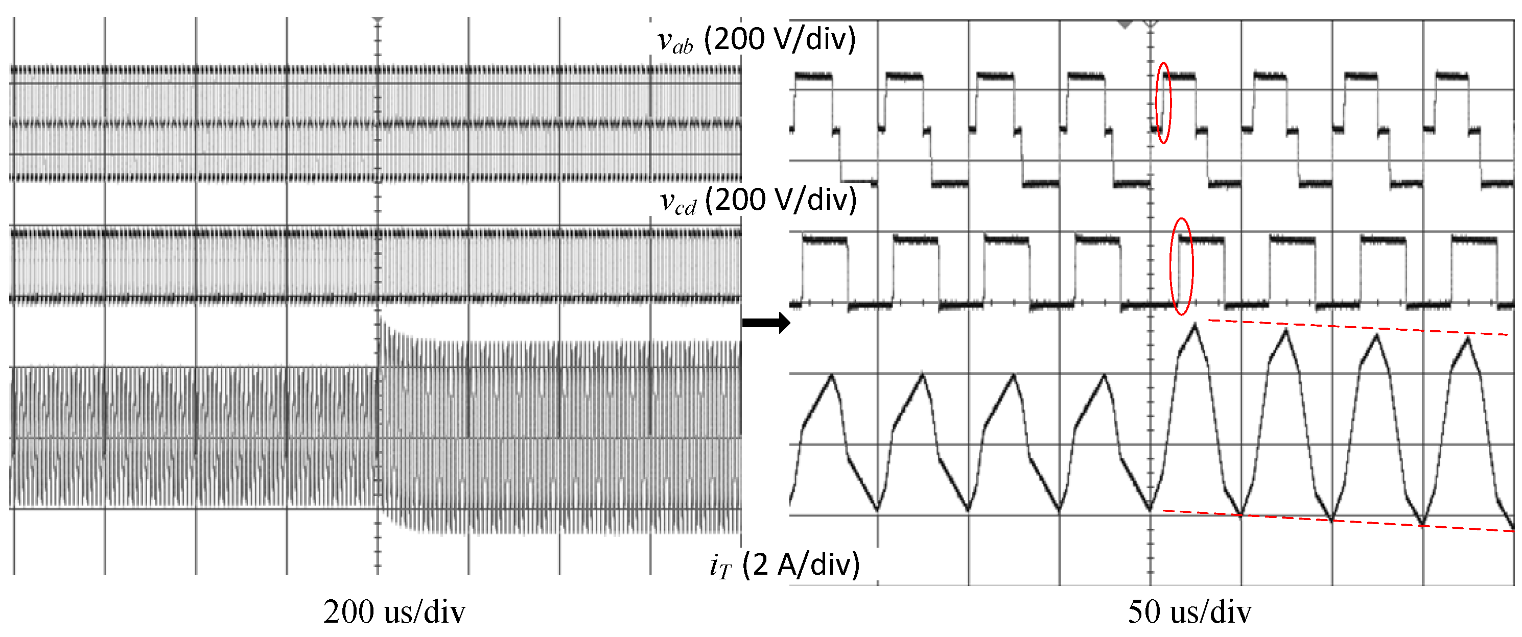
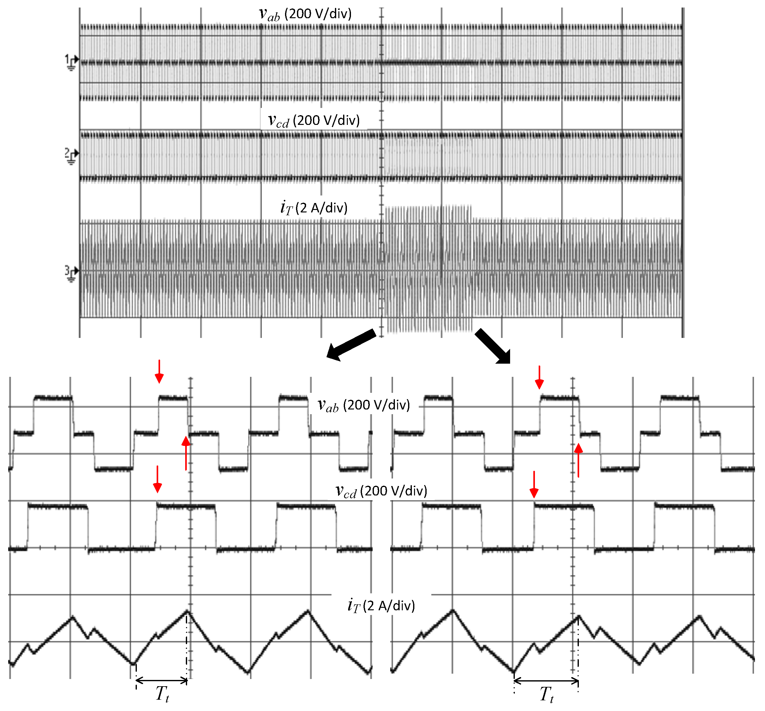
As shown in Figure 14, the first test case is the transition of {A, A} using DTM as a comparison benchmark. The original phase-shifts are at 100 W and the increments are . As seen in the upper part of Figure 14 (time scale 200s/div), the peak value of jumps from 1.95 A–3.52 A abruptly, which would results in a temporal DC bias current at 0.78 A. The envelope of then moves down gradually until it enters into the new steady state with an amplitude at 2.73 A at 130 W. The total transient process lasts for about 100s. The amplified detail of the process can be observed in the lower part of Figure 14 with a time scale of 10s/div. By referring to the rising edge of (from –0), the rising edge of (from 0–) and the rising edge of are delayed from their original positions by , , respectively. The tendency of to decay slowly after the modification of gating signals can be identified clearly. As seen in Figure 15, the similar long transition process with DC bias current also happens in the transition of {A, B} and {B, B} if DTM is still adopted.
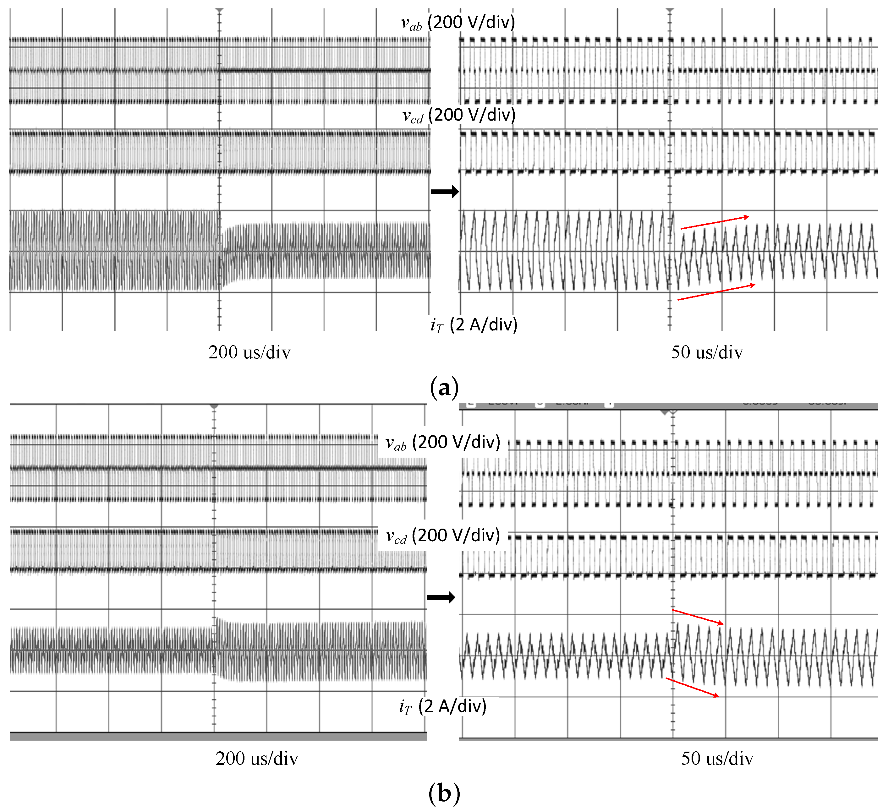
In Figure 16, Figure 17, Figure 18 and Figure 19, the experimental plots of the transition cases using the proposed FTM are presented. In each test case, the converter undergoes two consecutive opposite transitions with a time interval of 300s in between. In each figure, the upper part gives the view of the two consecutive transitions in a large time scale of 200s/div. The amplified view of each transition will be demonstrated in the lower part in a small time scale of 5s/div.
In Figure 16, the conditions of the first transition are the same as those in Figure 14, while the following second transition is the reverse process of the first one. According to Equation (12), and , . When the power is increased from 100 W–130 W, the rising edge (from 0–) and the following falling edge (from –0) of are shifted earlier by and respectively, which realizes the adjustment of to . Meanwhile, the rising edge of is delayed by , which realizes the adjustment of to . It can be seen from the current envelope that is always symmetric about the x-axis, though its amplitude undergoes two changes. Thus, the two transitions are completed almost instantly without introducing overshoot current and non-zero DC bias.
A shown in Figure 17, another example of the Type I case is the transition of {B, B}, in which the power level is increased from 25 W–60 W and then changed back. The initial phase-shifts are , and the increments are . The conditions for the power up transition are same as those in Figure 15 using DTM. With the help of FTM, the adjustments to the two edges of are and , respectively, and the adjustment to the rising edge of is . After 300 s, the process is reversed, and the converter is back to the initial steady state instantly. From both the envelope and the detail of current during the transient process, it can be seen that the adopted FTM effectively completes the transition as predicted in a fast and smooth way.
The measured plots shown in Figure 18 are for the transition of {A, B} and {B, A}. The conditions of {A, B} are the same as those in Figure 15 using DTM. The phase-shifts at 100 W (Mode A) are , and the phase-shifts at 55 W (Mode B) are . In the transition of {A, B}, the required adjustments are calculated as and , , while in the reverse process of {B, A}, the polarities of those values should be reversed. It can be seen that the peak current has two step changes from 1.95 A–1.36 A and then back to 1.95 A without any delay.
Experimental plots of transitions between two modes at negative power, {A, B} and {B, A}, are presented in Figure 19. The phase-shifts at high power W (Mode A) are , and the phase-shifts at low power W (Mode B) are . In the transition of {A, B}, the required adjustments are and , , while the polarities of those values should be reversed in the transition of {B, A}. Both transitions start from the falling edge of (from 0–). The difference is that lasts for four time interval intervals in {A, B} and five time intervals in {B, A}. The inductor current amplitude jumps from 2.52 A–1.19 A and jumps back after 30 HF periods. No noticeable overshoot current is observed from the current envelope at the transition moments.
According to the experimental plots, FTM shows satisfactory performance, which proves it to be a simple and easy-to-use solution. It is true that ZVS is not maintained for some switches for some cases from the experimental plot. However, this is the inherent feature of the steady-state mode itself. The application of FTM aims to achieve a fast load transition process without DC offset and does not bring extra switching loss. It is the duty of the phase-shit selector to choose a soft-switching control route.
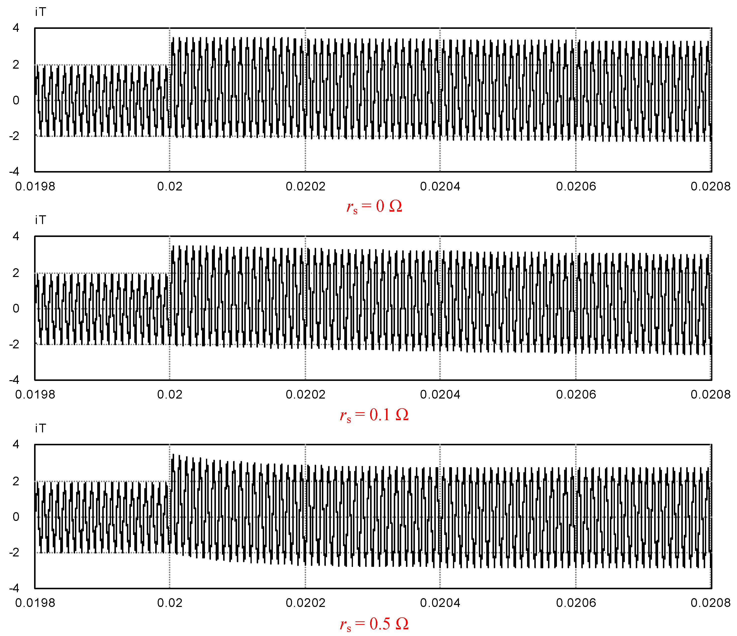
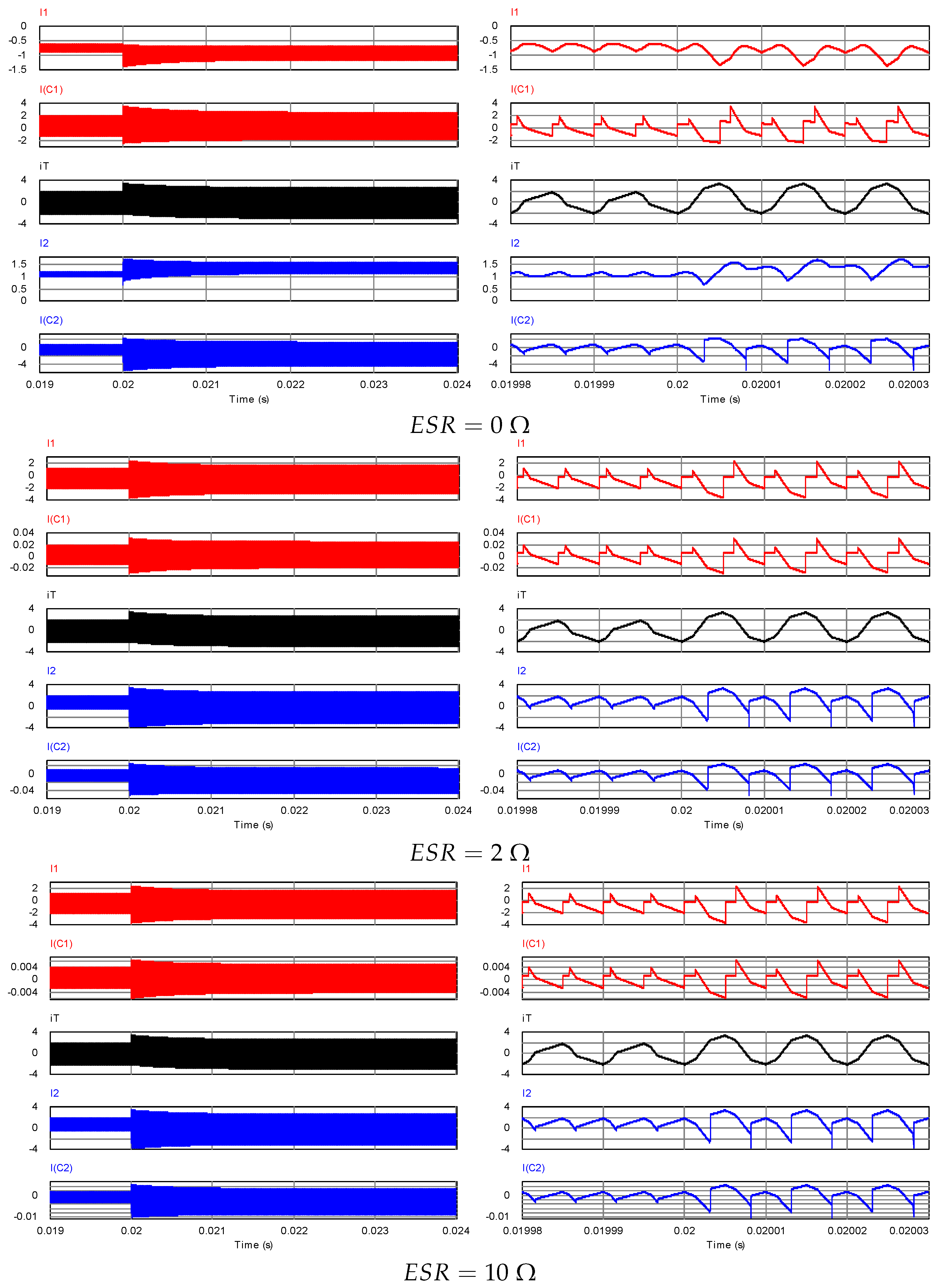
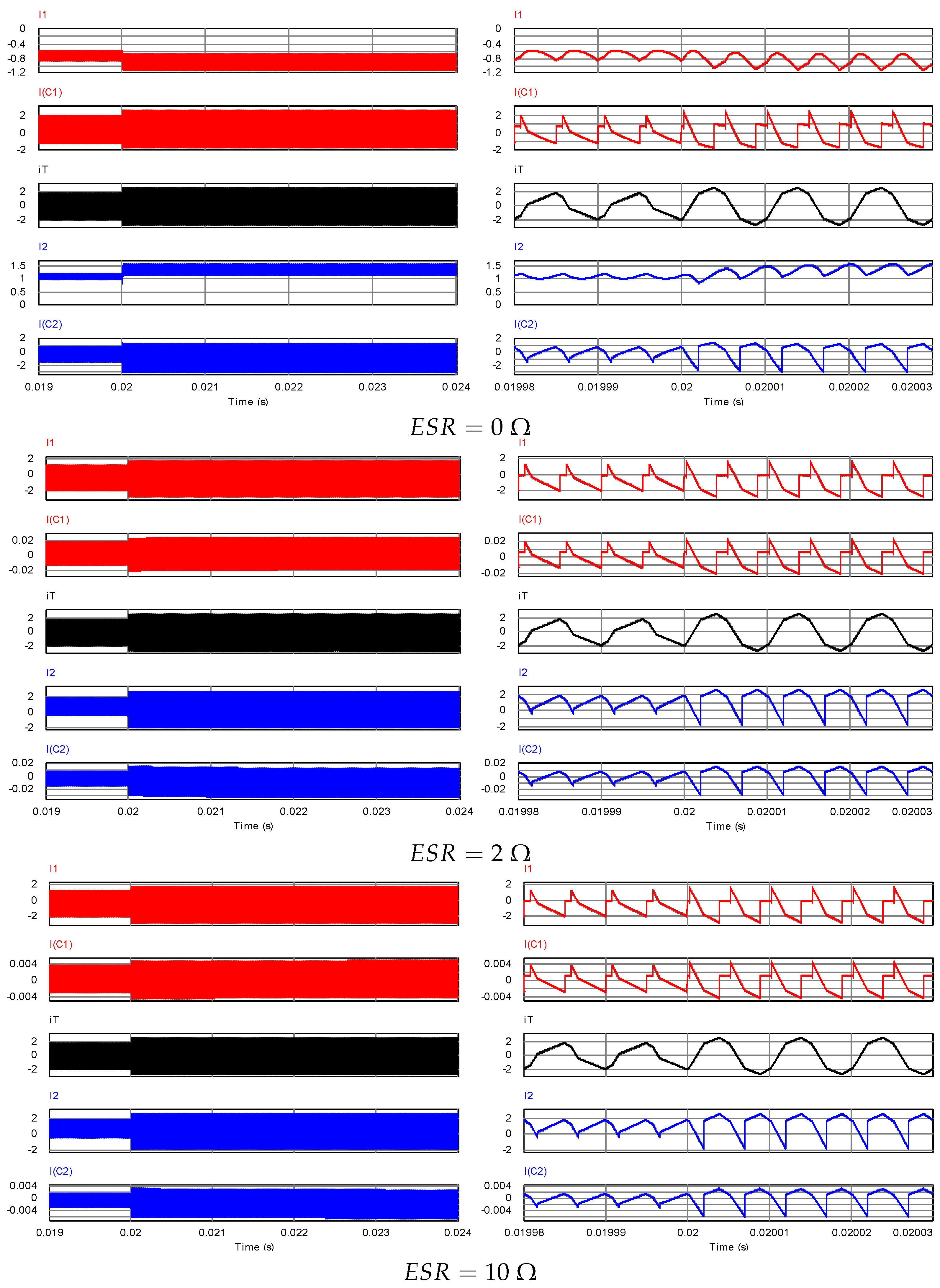
Theoretically, the existence of ESR (equivalent series resistance) of filter capacitors may affect the dynamic response of the capacitor voltage and consequentially affect the inductor current. In real applications, small ESR can be realized by parallel connection of electrolytic capacitors with large ESR and film capacitors with low ESR. To check the effect of filter capacitor ESR, three cases with different ESR values of and are evaluated for both DTM and FTM in simulation. It is assumed that the ESRs of and are the same, which are assumed to be , respectively. The plots of the transformer current , (current of ) and (current of ), (current of ) and (current of ) are displayed together. Besides, the internal resistance for both and are set at 0.2 in the simulation. According to Figure 20 and Figure 21, the effect of ESR on the inductor current is negligible for both steady state or transient response with either DTM or FTM. Due to the the non-zero ESR, the current ripples becomes higher in the two voltage sources. On the other side, the voltage source currents and show better dynamic response if the proposed FTM is applied regardless of the value of ESR of , , which is attributed to the improved transient response of .
5. Conclusions
In this paper, a transient modulation is proposed to realize fast and smooth transition at load changing in a DAB converter with EPS control. With this transient modulation, the required adjustments of involved gating signals are completed in less than one HF period in a specialized manner so that no overshoot current and DC bias will arise during the process. The key point lies in that the adjustments to the two phase-shift angles are distributed to different switch arms referred to a reference with a floating position , whose value is dependent on the converter voltage gain and the two phase-shift increments. The calculation of has a quite simple and universal expression regardless of the involved different operation modes in the transition, which makes it easy to implement in any micro-controller-based control platform. It is seen that the accuracy of relies on the precise measurement of the voltage levels of the two voltage sources in real-time mode and the phase-shift angle increments given by the adopted optimized control strategy. Thus, the proposed FTM may be incorporated with other close-loop control for execution of the orders given by the main controller, which deserves more efforts in the future. Moreover, the basic idea of the proposed FTM could be extended to TPS possibly to cope with the adjustments of three different phase-shift angles.
Author Contributions
C.S. did most of the theoretical analysis, derivation, circuit implementation, experimental testing and paper writing. X.L. was responsible for planning, coordination and proof reading.
Funding
This research was funded by Fundo para o Desenvolvimento das Ciências e da Tecnologia (060/2017/A).
Conflicts of Interest
The authors declare no conflict of interest.
References
- De Doncker, R.W.; Divan, D.M.; Kheraluwala, M.H. A three-phase soft-switched high power density DC/DC converter for high power applications. IEEE Trans. Ind. Appl. 1991, 27, 63–73. [Google Scholar] [CrossRef]
- Bal, S.; Rathore, A.K.; Srinivasan, D. Naturally Commutated Current-fed Three-Phase Bidirectional Soft-switching DC-DC Converter With 120∘ Modulation Technique. IEEE Trans. Ind. Appl. 2016, 52, 4354–4364. [Google Scholar] [CrossRef]
- Kheraluwala, M.H.; Gascoigne, R.; Divan, D.M.; Baumann, E. Performance characterization of a high power dual active bridge DC-to-DC converter. IEEE Trans. Ind. Appl. 1992, 28, 1294–1301. [Google Scholar] [CrossRef]
- Wang, Y.-C.; Ni, F.-M.; Lee, T.-L. Hybrid Modulation of Bidirectional Three-Phase Dual-Active-Bridge DC Converters for Electric Vehicles. Energies 2016, 9, 492. [Google Scholar] [CrossRef]
- Everts, J. Design and optimization of an efficient (96.1%) and compact (2 kW/dm3) bidirectional isolated single-phase dual active bridge AC-DC converter. Energies 2016, 9, 799. [Google Scholar] [CrossRef]
- Shi, X.; Jiang, J.; Guo, X. An efficiency-optimized isolated bidirectional DC-DC converter with extended power range for energy storage systems in microgrids. Energies 2012, 6, 27–44. [Google Scholar] [CrossRef]
- Pan, X.; Rathore, A.K. Novel Bidirectional Snubberless Naturally Commutated Soft-Switching Current-Fed Full-Bridge Isolated DC/DC Converter for Fuel Cell Vehicles. IEEE Trans. Ind. Electron. 2014, 61, 2307–2315. [Google Scholar]
- Rathore, A.K.; Prasanna, U.R. Analysis, Design, and Experimental Results of Novel Snubberless Bidirectional Naturally Clamped ZCS/ZVS Current-Fed Half-Bridge DC/DC Converter for Fuel Cell Vehicles. IEEE Trans. Ind. Electron. 2013, 60, 4482–4491. [Google Scholar] [CrossRef]
- Inoue, S.; Akagi, H. A bidirectional isolated DC-DC converter as a core circuit of the next-generation medium-voltage power conversion system. IEEE Trans. Power Electron. 2007, 22, 535–542. [Google Scholar] [CrossRef]
- Krismer, F.; Kolar, J. Accurate power loss model derivation of a highcurrent dual active bridge converter for an automotive application. IEEE Trans. Ind. Electron. 2010, 57, 881–891. [Google Scholar] [CrossRef]
- Mi, C.; Bai, H.; Wang, C.; Gargies, S. Operation, design and control of dual h-bridge-based isolated bidirectional DC-DC converter. IET Power Electron. 2008, 1, 507–517. [Google Scholar] [CrossRef]
- Zhao, B.; Yu, Q.; Sun, W. Extended-phase-shift control of isolated bidirectional DC-DC converter for power distribution in microgrid. IEEE Trans. Power Electron. 2012, 27, 4667–4680. [Google Scholar] [CrossRef]
- Wen, H.; Xiao, W.; Su, B. Nonactive power loss minimization in a bidirectional isolated DC-DC converter for distributed power systems. IEEE Trans. Ind. Electron. 2014, 61, 6822–6831. [Google Scholar] [CrossRef]
- Oggier, G.G.; Garcia, G.O.; Oliva, A.R. Modulation strategy to operate the dual active bridge DC-DC donverter under soft switching in the whole operating range. IEEE Trans. Power Electron. 2011, 26, 1228–1236. [Google Scholar] [CrossRef]
- Oggier, G.G.; Garcia, G.O.; Oliva, A.R. Switching control strategy to minimize dual active bridge converter losses. IEEE Trans. Power Electron. 2009, 24, 1826–1838. [Google Scholar] [CrossRef]
- Jain, A.K.; Ayyanar, R. PWM control of dual active bridge: Comprehensive analysis and experimental verification. IEEE Trans. Power Electron. 2011, 26, 1215–1227. [Google Scholar] [CrossRef]
- Krismer, F.; Kolar, J. Efficiency-optimized high-current dual active bridge converter for automotive applications. IEEE Trans. Ind. Electron. 2012, 59, 2745–2760. [Google Scholar] [CrossRef]
- Zhao, B.; Song, Q.; Liu, W. Efficiency characterization and optimization of isolated bidirectional DC-DC converter based on dual-phase-shift control for DC distribution application. IEEE Trans. Power Electron. 2013, 28, 1711–1727. [Google Scholar] [CrossRef]
- Zhao, B.; Song, Q.; Liu, W. Power characterization of Isolated bidirectional dual-active-bridge DC-DC converter with dual-phase-shift control. IEEE Trans. Power Electron. 2012, 27, 4172–4176. [Google Scholar] [CrossRef]
- Bai, H.; Mi, C. Eliminate reactive power and increase system efficiency of isolated bidirectional dual-active-bridge DC-DC converters using novel dual-phase-shift Control. IEEE Trans. Power Electron. 2008, 23, 2905–2914. [Google Scholar] [CrossRef]
- Zhao, B.; Song, Q.; Liu, W.; Sun, W. Current-stress-optimized switching strategy of isolated bidirectional DC-DC converter with dual-phase-shift control. IEEE Trans. Ind. Electron. 2013, 60, 4458–4467. [Google Scholar] [CrossRef]
- Wu, K.; de Silva, C.W.; Dunford, W.G. Stability analysis of isolated bidirectional dual active full-bridge DC-DC converter with triple phase-shift control. IEEE Trans. Power Electron. 2012, 27, 2007–2017. [Google Scholar] [CrossRef]
- Krismer, F.; Kolar, J.W. Closed form solution for minimum conduction loss modulation of dab converters. IEEE Trans. Power Electron. 2012, 27, 174–188. [Google Scholar] [CrossRef]
- Huang, J.; Wang, Y.; Li, Z.; Lei, W. Unified triple-phase-shift control to minimize current stress and achieve full soft-switching of isolated bidirectional DC-DC converter. IEEE Trans. Ind. Electron. 2016, 63, 4169–4179. [Google Scholar] [CrossRef]
- Engel, S.P.; Soltau, N.; Stagge, H.; de Doncker, R.W. Dynamic and Balanced Control of Three-Phase High-Power Dual-Active Bridge DC-DC Converters in DC-Grid Applications. IEEE Trans. Power Electron. 2013, 28, 1880–1889. [Google Scholar] [CrossRef]
- Li, X.; Li, Y.-F. An optimized phase-shift modulation for fast transient response in a dual-active-bridge converter. IEEE Trans. Power Electron. 2014, 29, 2661–2665. [Google Scholar] [CrossRef]
- Lin, S.-T.; Li, X.; Sun, C.; Tang, Y. Fast transient control for power adjustment in a dual-active-bridge converter. Electron. Lett. 2017, 53, 1130–1132. [Google Scholar] [CrossRef]
- Zhao, B.; Song, Q.; Liu, W.; Zhao, Y. Transient DC Bias and Current Impact Effects of High-Frequency-Isolated Bidirectional DC-DC Converter in Practice. IEEE Trans. Power Electron. 2016, 31, 3203–3216. [Google Scholar] [CrossRef]
- Takagi, K.; Fujita, H. Dynamic Control and Performance of a Dual-Active-Bridge DC-DC Converter. IEEE Trans. Power Electron. 2017. [Google Scholar] [CrossRef]
- Li, Z.; Wang, Y.; Cui, Y.; Shi, L.; Huang, J.; Lei, W. Fast Transient Current Control for Three-Phase Dual-Active-Bridge DC-DC Converters with Variable Duty Cycles. In Proceedings of the IEEE Applied Power Electronics Conference and Exposition (APEC), Tampa, FL, USA, 26–30 March 2017. [Google Scholar]
- Ortiz, G.; Fassler, L.; Kolar, J.W.; Apeldoorn, O. Flux Balancing of Isolation Transformers and Application of “The Magnetic Ear” for Closed-Loop Volt-Second Compensation. IEEE Trans. Power Electron. 2014, 29, 4078–4090. [Google Scholar] [CrossRef]
Figure 1.
The circuit schematic of a DAB DC/DC converter with its steady-state equivalent circuit.
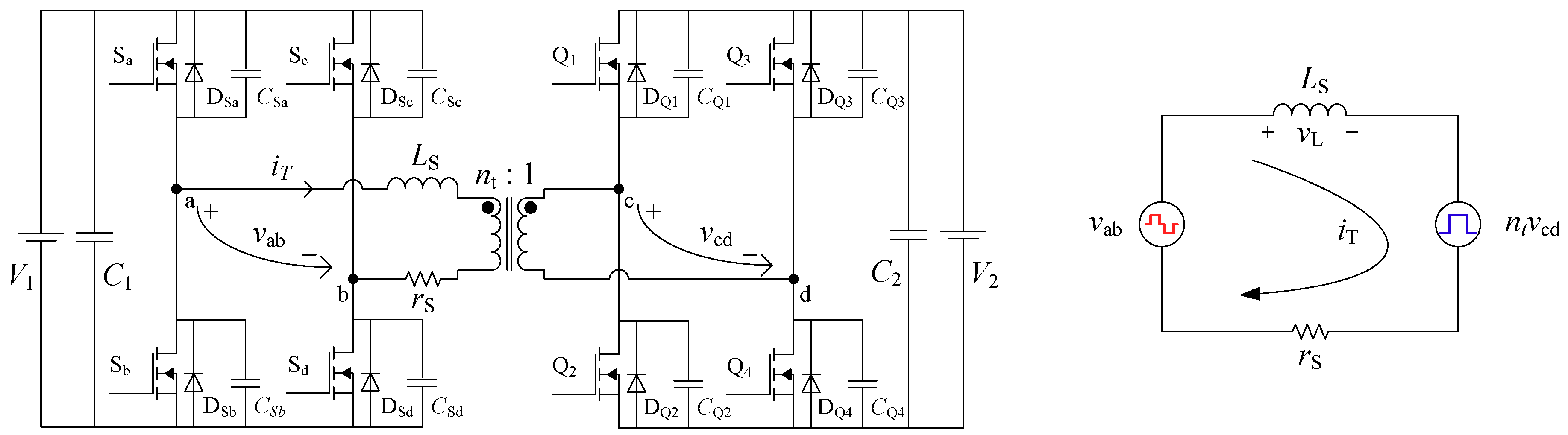
Figure 2.
Steady-state operation modes with EPS control.
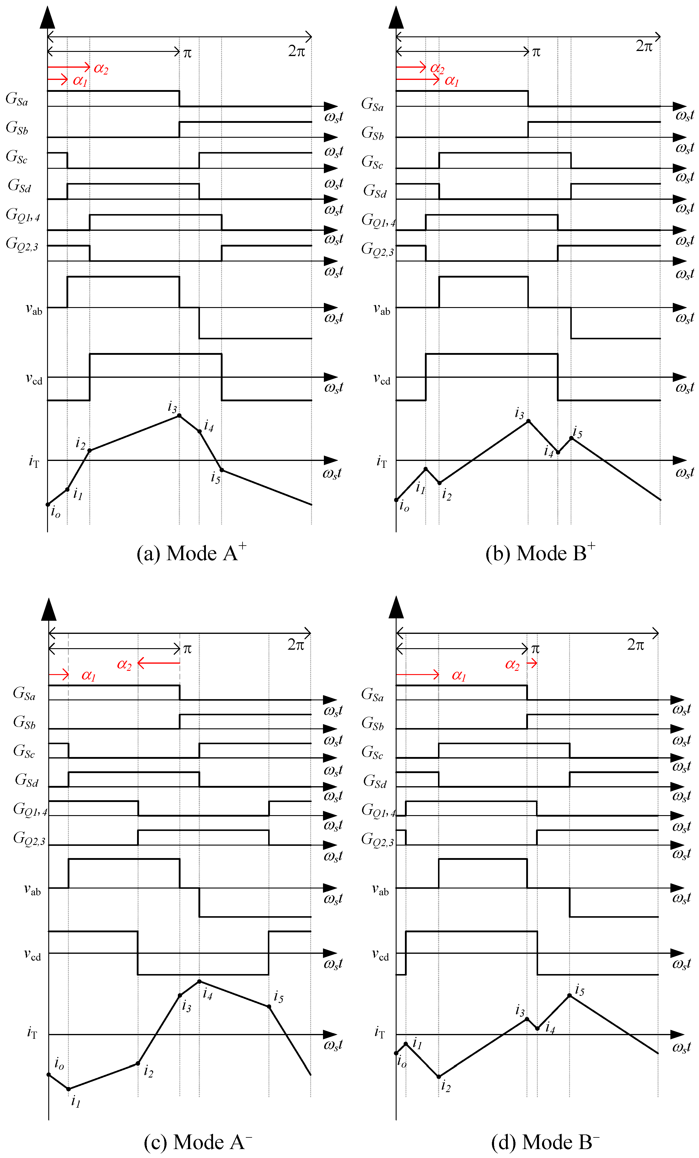
Figure 3.
Ranges of phase-shift angles in each mode.

Figure 4.
A transition of {A, A} using DTM: (a) theoretical waveforms; (b) simulated waveforms.
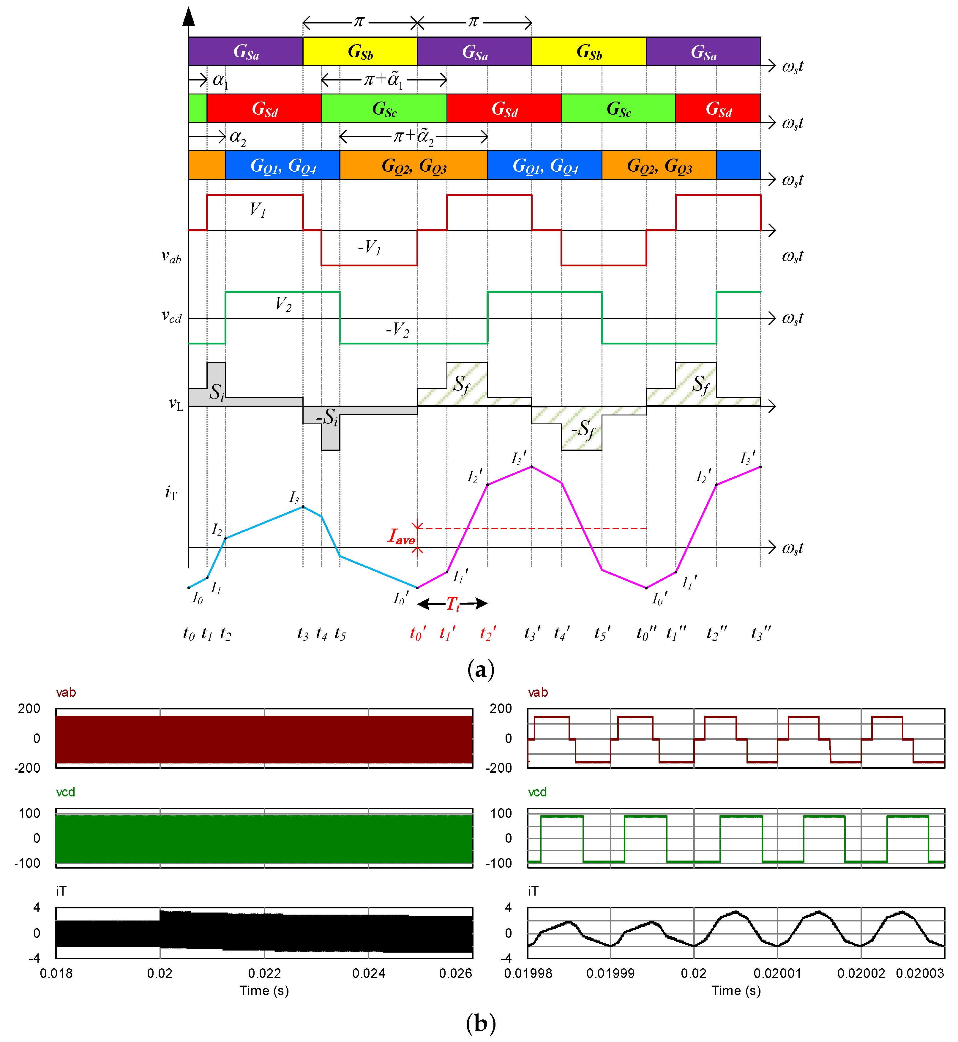
Figure 5.
A transition of {A, A} using DTM with different .

Figure 6.
Example of Type I: {A, A} using fast transient modulation (FTM): (a) theoretical plots; (b) simulated plots.
Figure 6.
Example of Type I: {A, A} using fast transient modulation (FTM): (a) theoretical plots; (b) simulated plots.
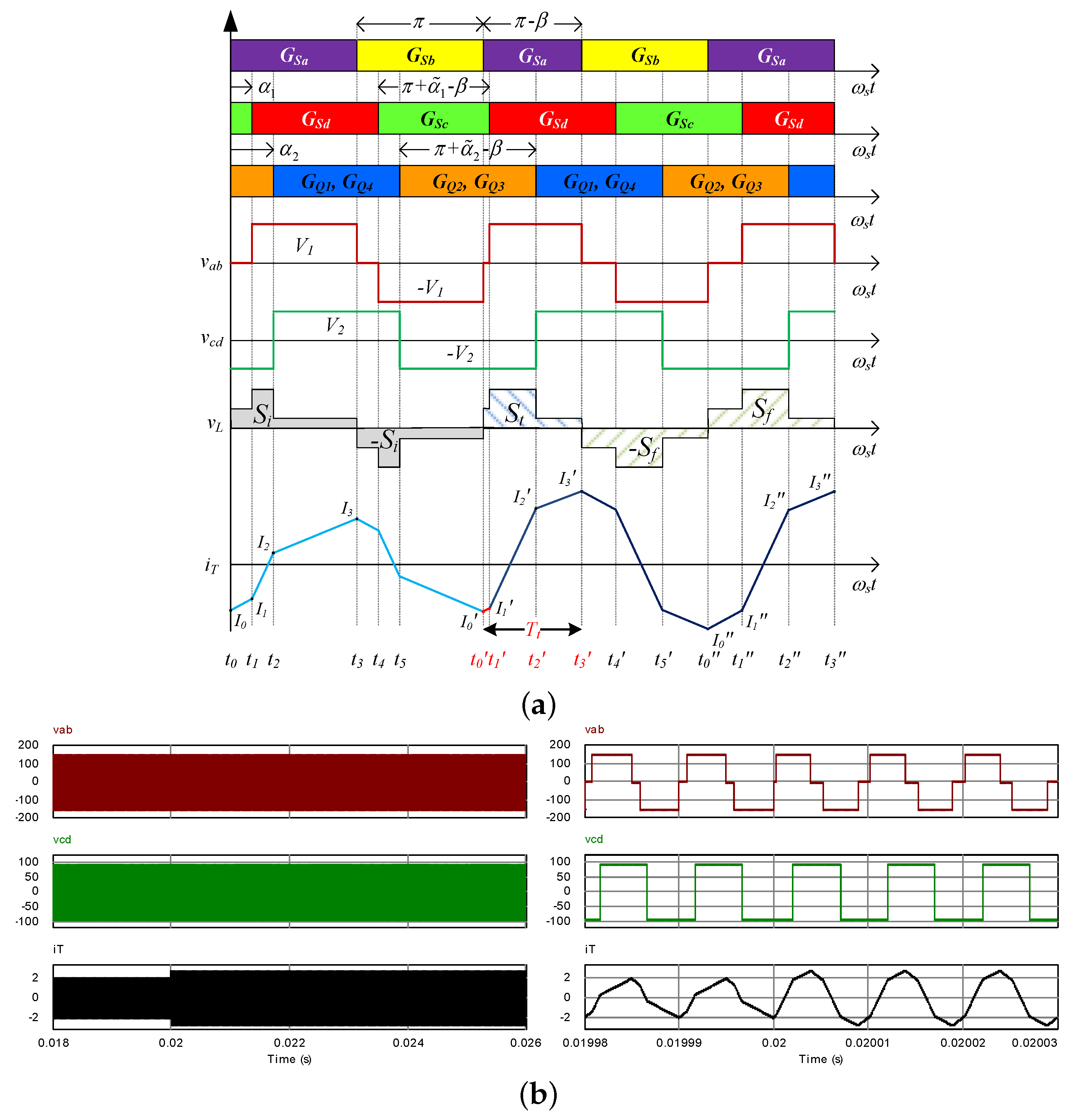
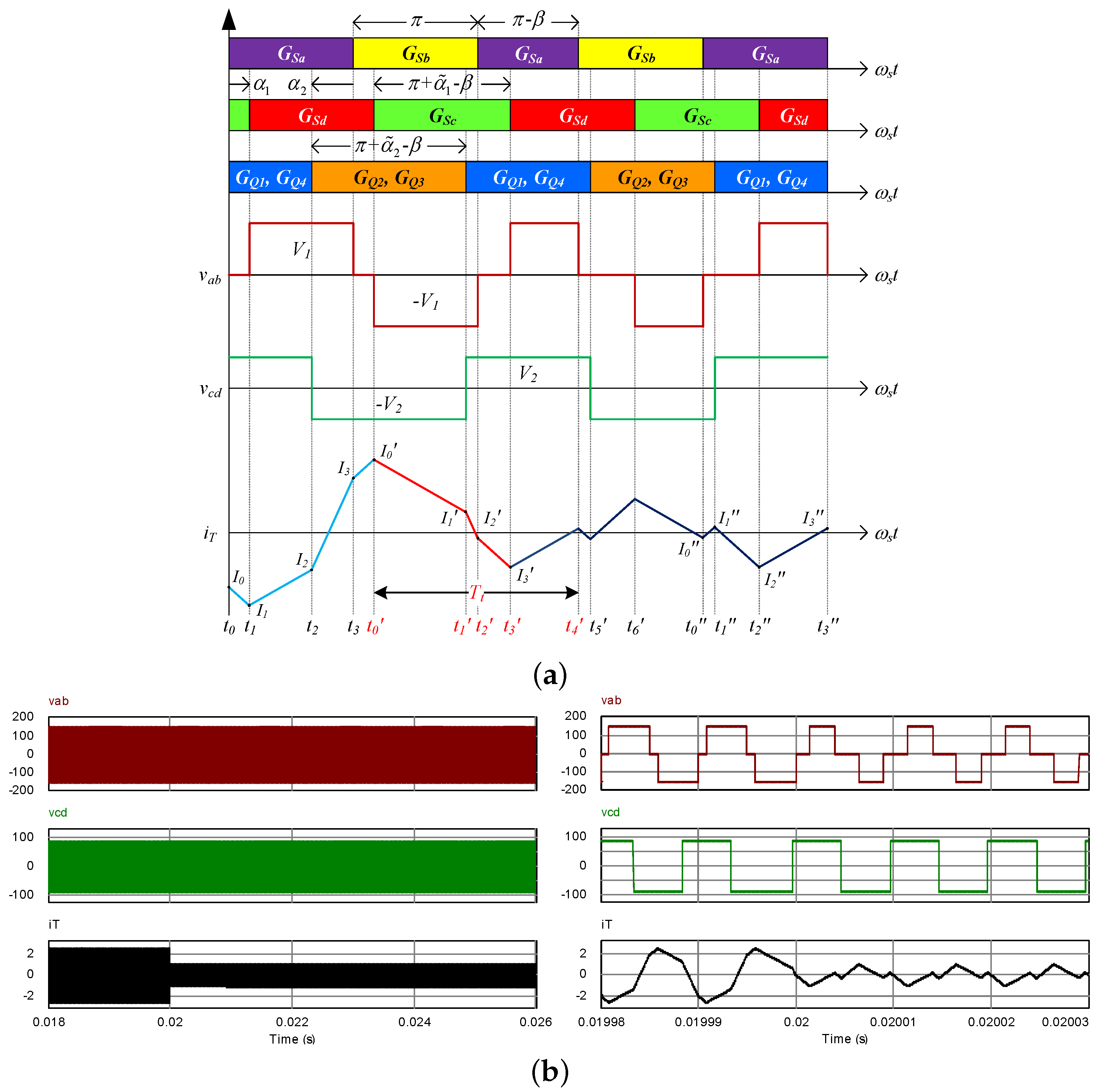
Figure 7.
Example of Type II: {A, B} using FTM: (a) theoretical plots; (b) simulation plots.

Figure 8.
Example of Type II: {A, B} (a) theoretical plots; (b) simulation plots.

Figure 9.
Examples of Category III: {A, A}. (a) theoretical plots; (b) simulation plots.

Figure 10.
Photo of the experimental setup.
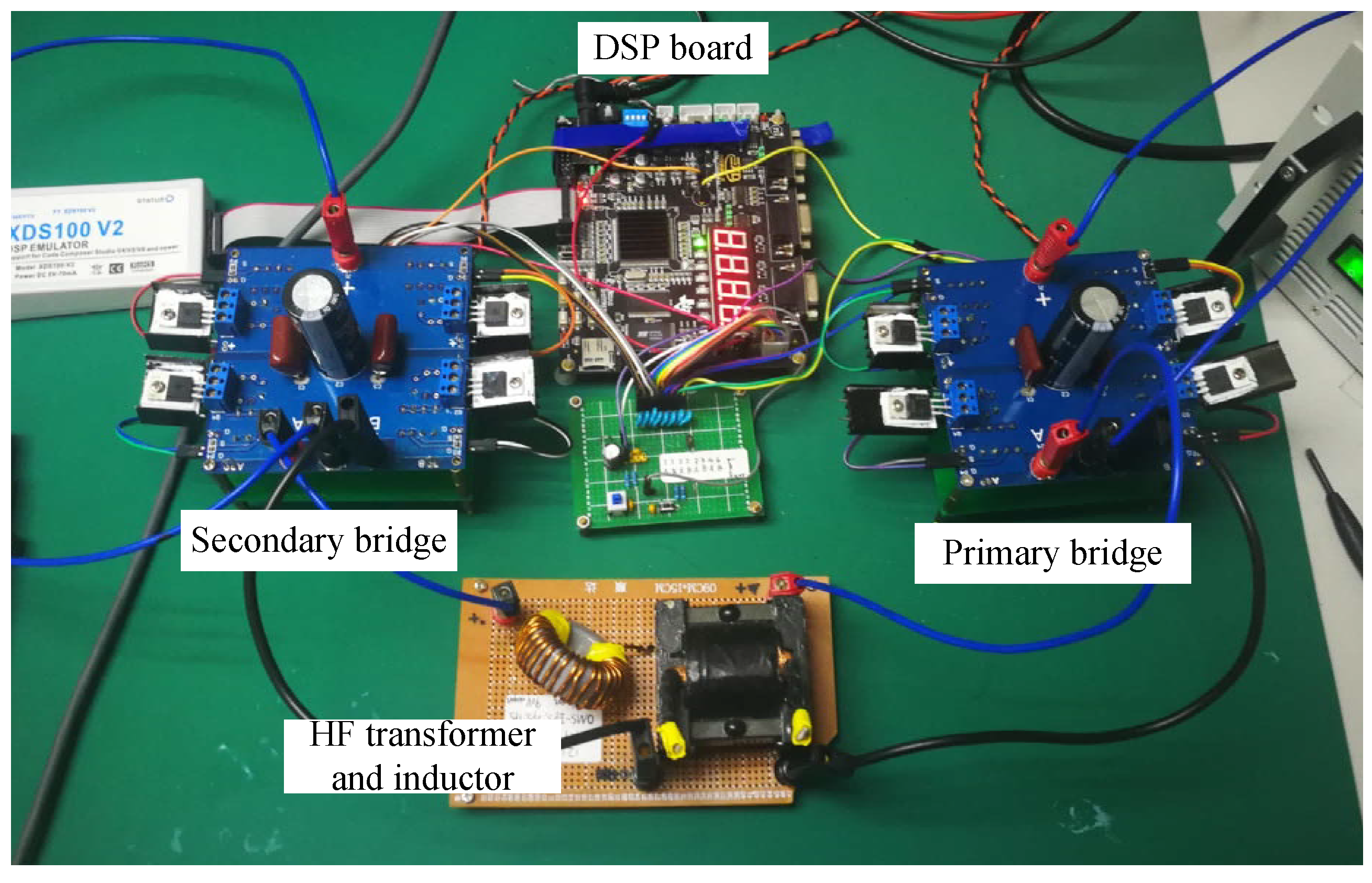
Figure 11.
Implementation of fast transient modulation (FTM) using a DSP development board.
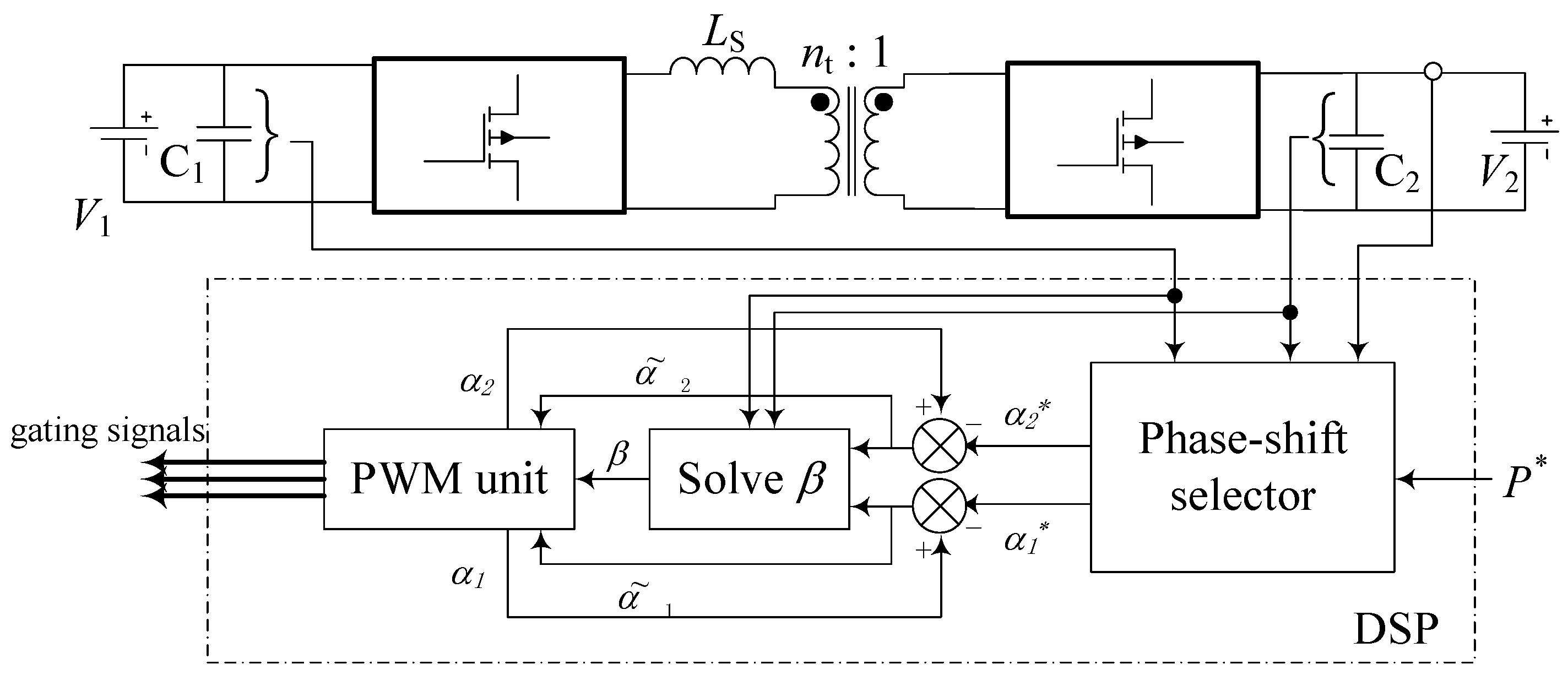
Figure 12.
The flowchart of DSP control program.
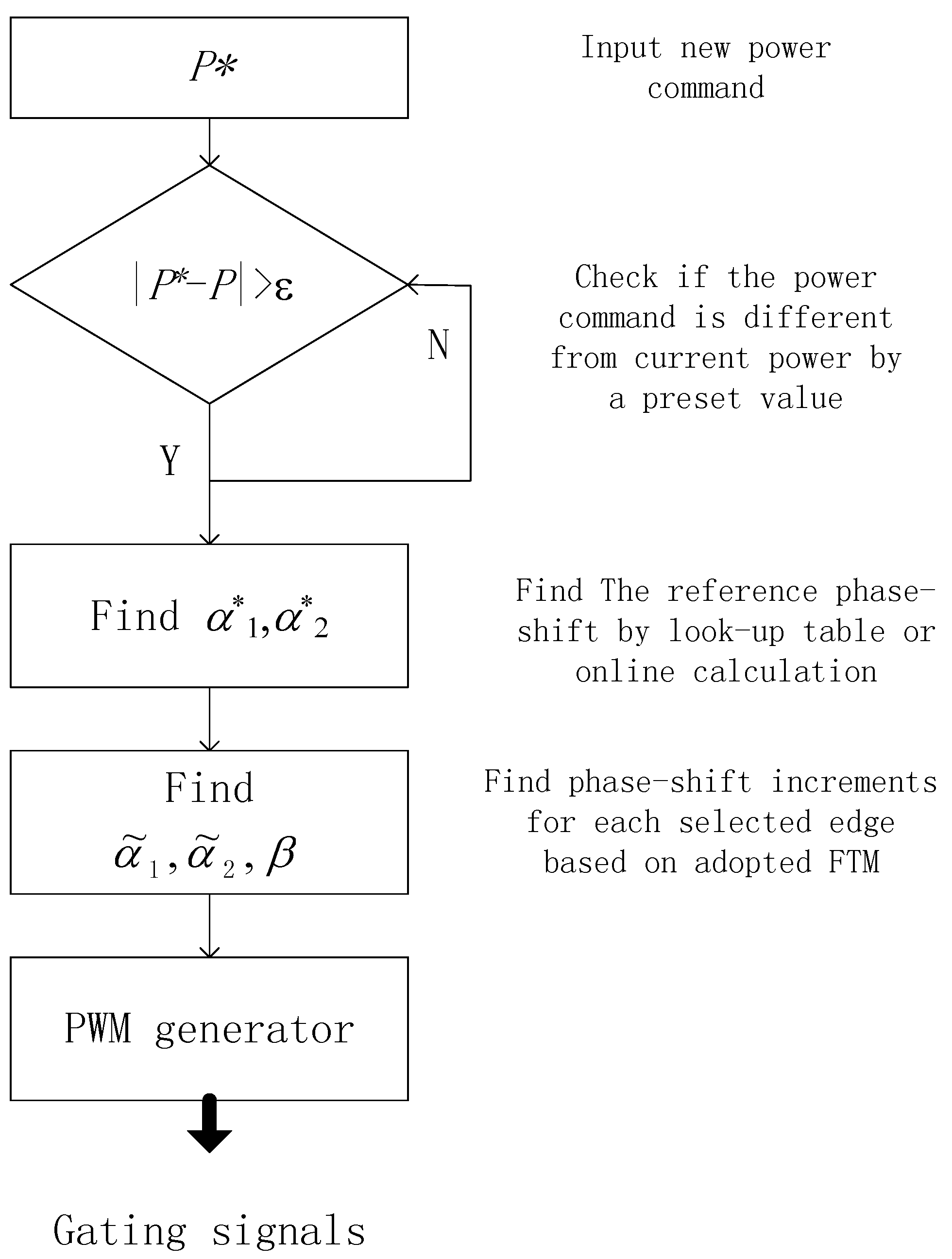
Figure 13.
Principles of the PWM unit in the DSP board.
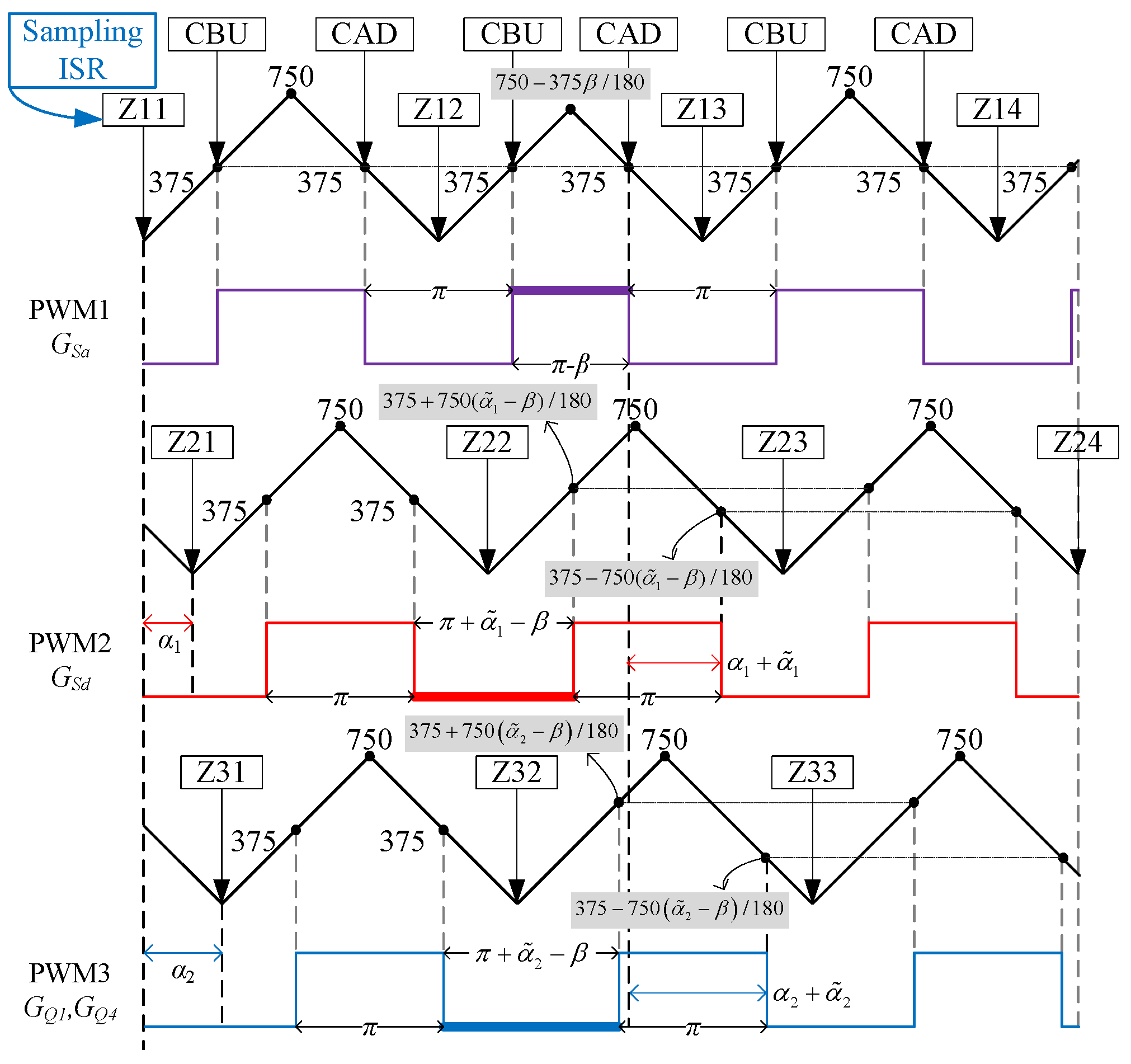
Figure 14.
Experimental plots of the transition {A, A} using DTM.

Figure 15.
Experimental plots of the transition (a) {A, B} and (b) {B, B} using DTM.

Figure 16.
Experimental plots of the transition {A, A} using FTM; the time scale is 200s/div (top) and 5s/div (bottom).
Figure 16.
Experimental plots of the transition {A, A} using FTM; the time scale is 200s/div (top) and 5s/div (bottom).
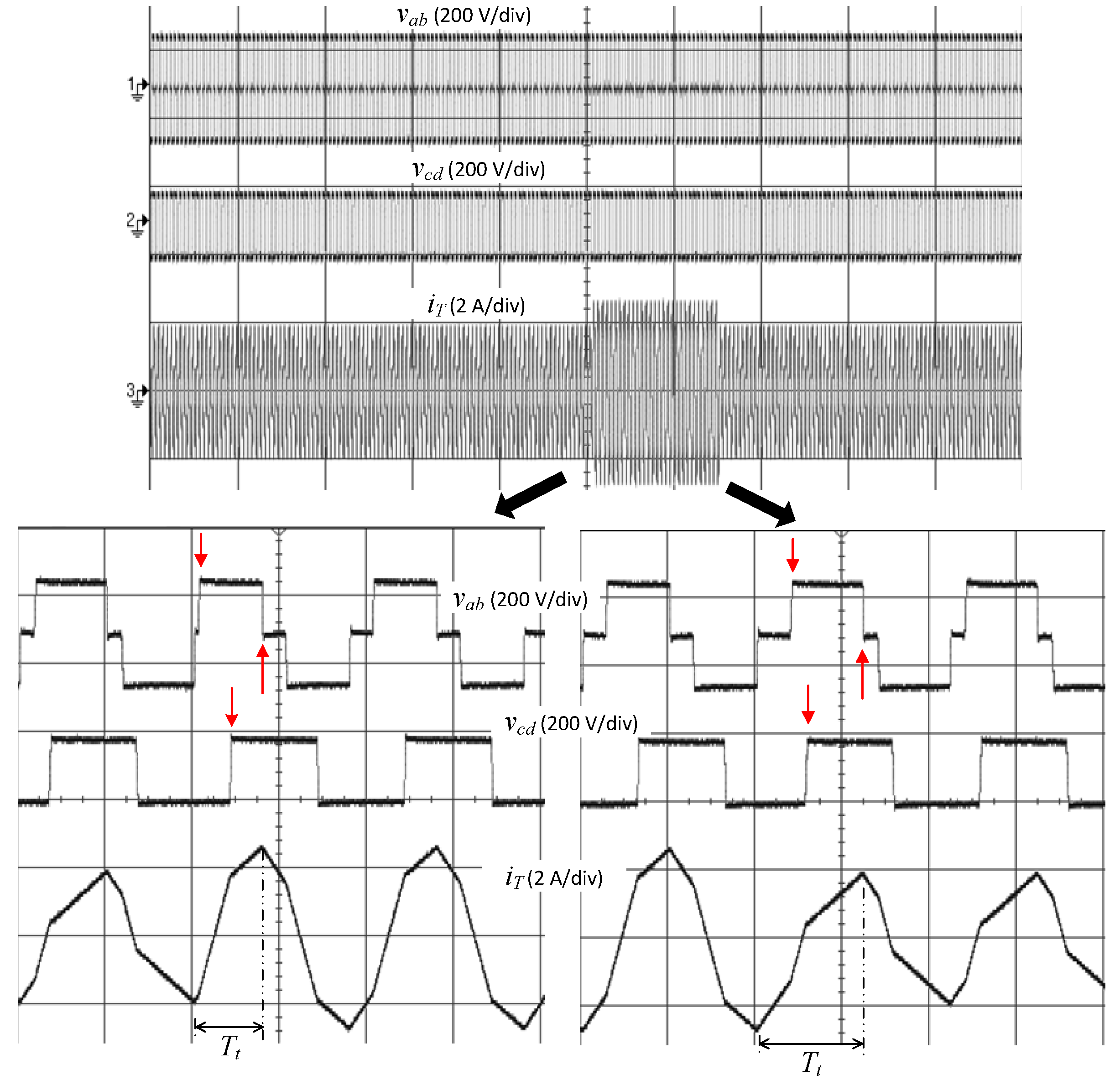
Figure 17.
Experimental plots of the transition {B, B} using FTM; the time scale is 200s/div (top) and 5s/div (bottom).
Figure 17.
Experimental plots of the transition {B, B} using FTM; the time scale is 200s/div (top) and 5s/div (bottom).

Figure 18.
Experimental plots of the transition {A, B} and {B, A} using FTM; the time scale is 200s/div (top) and 5s/div (bottom).
Figure 18.
Experimental plots of the transition {A, B} and {B, A} using FTM; the time scale is 200s/div (top) and 5s/div (bottom).
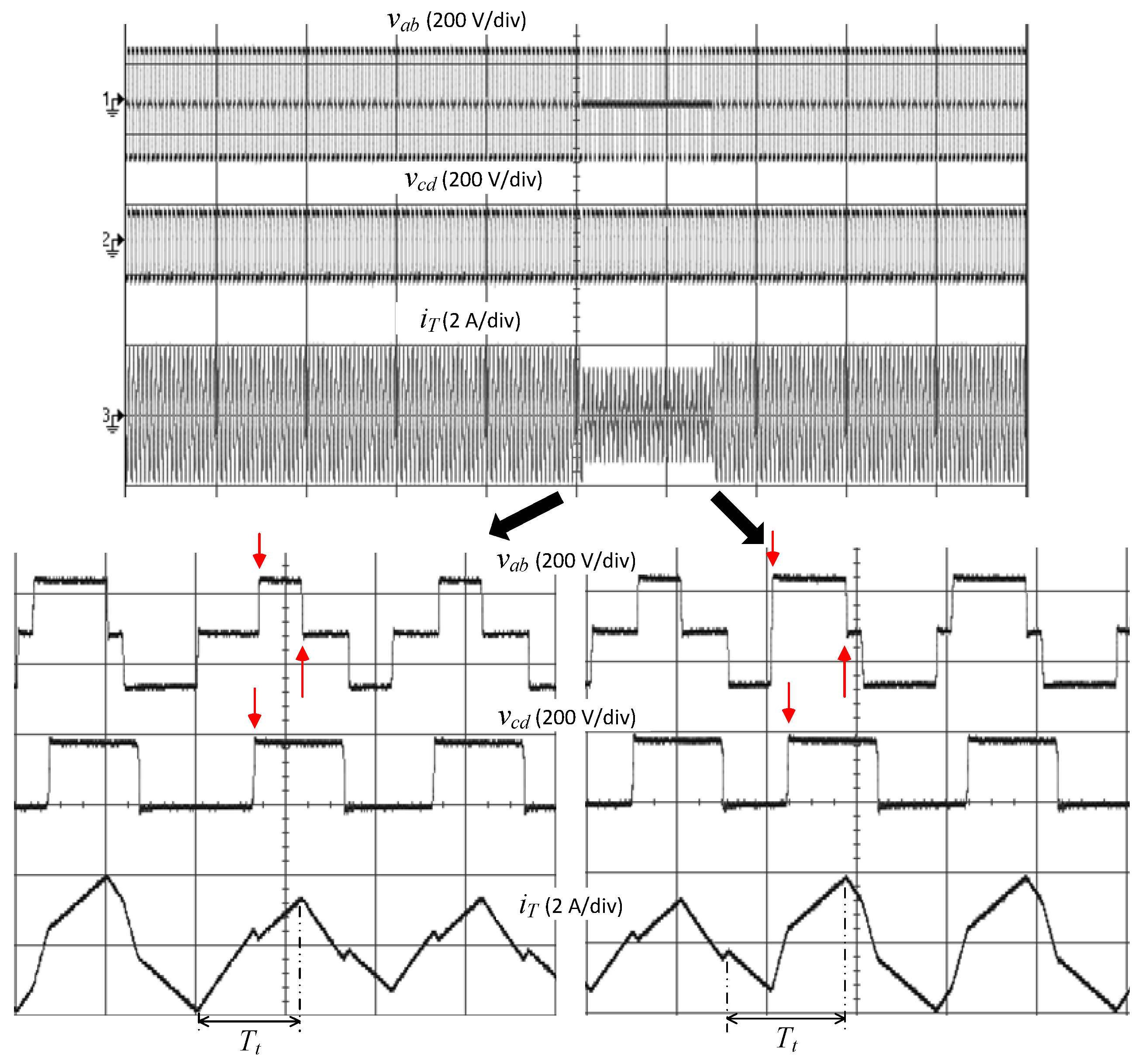
Figure 19.
Experimental plots of the transition {A, B} and {B, A} using FTM; the time scale is 200s/div (top) and 5s/div (bottom).
Figure 19.
Experimental plots of the transition {A, B} and {B, A} using FTM; the time scale is 200s/div (top) and 5s/div (bottom).
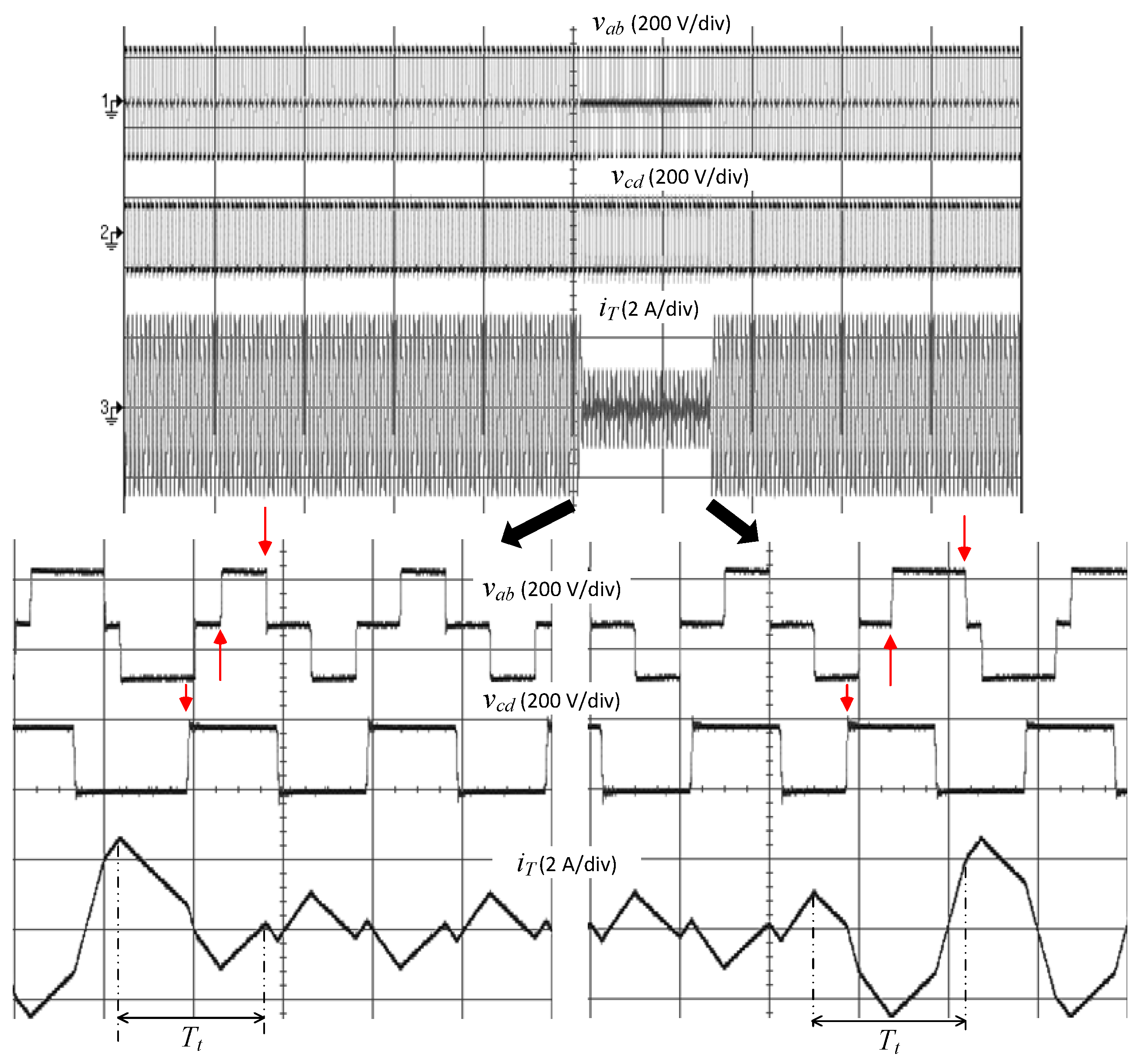
Figure 20.
Simulation plots of the transition {A, A} using DTM with different equivalent series resistances (ESRs) of the filter capacitor.
Figure 20.
Simulation plots of the transition {A, A} using DTM with different equivalent series resistances (ESRs) of the filter capacitor.

Figure 21.
Simulation plots of the transition {A, A} using FTM with different ESRs of the filter capacitor.
Figure 21.
Simulation plots of the transition {A, A} using FTM with different ESRs of the filter capacitor.


Table 1.
Mode characteristics under extended-phase-shift (EPS).
| Mode | Normalized Instantaneous Currents |
|---|---|
| A | |
| A | |
| B, B | |
Table 2.
The key specifications of the experiment.
| Parameter | Symbol | Value |
|---|---|---|
| DC input voltage | 150 V | |
| DC output voltage | 90 V | |
| Transformer turns ratio | :1 | 1:1 |
| Transformer ferrite core | - | PC40ETD49 |
| Series inductor inductance | 121.8 H | |
| Inductor material | - | MPPcore, CM400125 |
| HF filter capacitance | , | 330 F |
| Primary-side MOSFETs | – | STP40NF20, 200 V, 40 A, 0.038 |
| Secondary-side MOSFETs | – | IPP200N15N3 G, 150 V, 50 A, 0.020 |
| Switching frequency | 100 kHz |
© 2018 by the authors. Licensee MDPI, Basel, Switzerland. This article is an open access article distributed under the terms and conditions of the Creative Commons Attribution (CC BY) license (http://creativecommons.org/licenses/by/4.0/).
Share and Cite
MDPI and ACS Style
Sun, C.; Li, X. Fast Transient Modulation for a Step Load Change in a Dual-Active-Bridge Converter with Extended-Phase-Shift Control. Energies 2018, 11, 1569. https://doi.org/10.3390/en11061569
AMA Style
Sun C, Li X. Fast Transient Modulation for a Step Load Change in a Dual-Active-Bridge Converter with Extended-Phase-Shift Control. Energies. 2018; 11(6):1569. https://doi.org/10.3390/en11061569
Chicago/Turabian StyleSun, Chuan, and Xiaodong Li. 2018. "Fast Transient Modulation for a Step Load Change in a Dual-Active-Bridge Converter with Extended-Phase-Shift Control" Energies 11, no. 6: 1569. https://doi.org/10.3390/en11061569
Note that from the first issue of 2016, this journal uses article numbers instead of page numbers. See further details here.