IGBT Dynamic Loss Reduction through Device Level Soft Switching

1
School of Automation Engineering, University of Electronic Science and Technology of China, West High-Tech District, Chengdu 611731, China
2
Department of Electrical and Computer Engineering, NC State University, Raleigh, NC 27695, USA
3
Department of Electrical and Computer Engineering, The University of Texas at Austin, Austin, TX 78712, USA
*
Author to whom correspondence should be addressed.
Energies 2018, 11(5), 1182; https://doi.org/10.3390/en11051182
Submission received: 30 March 2018
/
Revised: 3 May 2018
/
Accepted: 7 May 2018
/
Published: 8 May 2018
(This article belongs to the Special Issue Emerging Power Electronics Technologies for Power Systems and Machine Drives)
Abstract
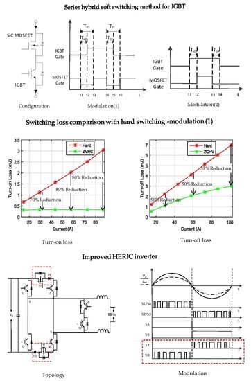
:Due to its low conduction loss, hence high current ratings, as well as low cost, Silicon Insulated Gate Bipolar Transistor (Si IGBT) is widely used in high power applications. However, its switching frequency is generally low because of relatively large switching losses. Silicon carbide Metal-Oxide-Semiconductor Field-Effect Transistor (SiC MOSFET) is much more superior due to their fast switching speed, which is determined by the internal parasitic capacitance instead of the stored charges, like the IGBT. By the combination of SiC MOSFET and Si IGBT, this paper presents a novel series hybrid switching method to achieve IGBT’s dynamic switching loss reduction by switching under Zero Voltage Hard Current (ZVHC) turn-on and Zero Current Hard Voltage (ZCHV) turn-off conditions. Both simulation and experimental results of IGBT are carried out, which shows that the soft switching of IGBT has been achieved both in turn-on and turn-off period. Thus 90% turn-on loss and 57% turn-off loss are reduced. Two different IGBTs’ test results are also provided to study the modulation parameter’s effect on the turn-off switching loss. Furthermore, with the consideration of voltage and current transient states, a new soft switching classification is proposed. At last, another improved modulation and Highly Efficient and Reliable Inverter Concept (HERIC) inverter are given to validate the effectiveness of the device level hybrid soft switching method application.
1. Introduction
The Si IGBT is one of the most important power semiconductor devices and is found in widespread high power applications, like medium voltage motor drives, EV traction inverters, and grid-connected inverters for PV and wind. To obtain high efficiency, high power density, and low junction temperatures, the switching losses must be kept low by fast switching of the IGBT [1]. However, under hard switching condition, the IGBT voltage and current have a substantial overlap during the turn-on and turn-off events that introduce significant switching losses, especially the switching-off loss. It exhibits a current tail during turn-off period that causes high turn-off switching loss, since IGBT is a minority-carrier device [2]. To reduce the switching loss, the design and optimization of IGBT is a non-stopping effort by device manufacturers, resulting in improved performance from one generation to another. One of the most effective ways to reduce the switching loss is manipulating the voltage and current waveforms of IGBT during the turn-on or off transition periods to eliminate or to reduce the overlap. There are two critical factors affects the voltage and current waveforms’ states of IGBT, which are the designs of gate driver circuit and the external circuit. A simple gate-boosting circuit is presented in [3], which achieved the reduction of current rise time and the turn-on loss. Moreover, based on the gate driver circuit, different open and closed loop control strategies have also been proposed. A multistage gate drive control concept has been proposed in [4,5] to realize the optimal turn-on and turn-off performance. According to the different feedback signals or constraints, adaptive feedback control [6] and dynamic gate current control [7] can also effectively reduce the IGBT switching loss with variable switching speed. By introducing the active voltage control technique and shaping the IGBT switching transient into a sophisticated ‘S’-shape, both switching loss reduction and acceptable Electromagnetic Interference (EMI) can be achieved in [8]. The main drawbacks that are associated with these methods are control complexity for accurate signals detection and limited switching loss reduction. Adding the auxiliary circuit is also a popular way to reduce the IGBT switching loss by achieving soft switching. A passive circuit, which is composed of an extra capacitor, inductor, and diode is one of the attractive ways to cut down the switching loss. By introducing an external capacitor that is paralleled with the IGBT, the voltage rise is softer during the turn-off transition, which results in the reduction of power loss [9,10]. In these papers, zero voltage switching ZVS is realized for the IGBT. However, the energy that is stored in the snubber capacitor is discharged through the IGBT, which causes a current spike during the turn-on transition. Adding an external inductor series with IGBT reduces the switching loss by achieving zero current switching [11,12]. However, it can result in an extra magnetic loss. There is also an active auxiliary circuit that includes the active switches to achieve IGBT soft switching. Varies approaches are proposed to reduce the switching loss of the main switches in the different application [13,14]. The cost of these active auxiliary circuits is higher when compared to the passive circuit. Also, to improve the efficiency of the application, the active switches should also operate under soft switching condition, which increases the control complexity [15]. With the help of the external circuit and various control strategies, the switching loss of IGBT can be efficiently reduced. However, there still a high cost for those solutions and the applicability is also limited.
When compared to the IGBT, the MOSFET has excellent switching characteristic. By combining the advantages of the MOSFET and the IGBT, a hybrid switch is proposed in [16], which are composed of an IGBT and a MOSFET. Based on the parallel connection of these two devices, the hybrid switch achieved better performance for the higher frequency. It also can improve the efficiency when introducing to different applications [17,18]. In recent years, emerging wide bandgap (WBG) devices, such as silicon carbide (SiC) MOSFET, provide an attractive solution to improve power converter efficiency and power density by reducing semiconductor losses, operating at higher switching frequencies, and higher temperatures in many different applications. However, the price of SiC MOSFET is usually three to five times of the same rating Si IGBT device [19]. Moreover, SiC unipolar devices strongly suffer from oscillatory behavior during turn-off switching due to the lack of excess carriers. To overcome these drawbacks, hybrid switches, which connect Si IGBT and SiC MOSFET in parallel were studied in [20,21,22]. The characteristics of hybrid switches have been analyzed in detail. Furthermore, with a comprehensive consideration of device losses, reliable operation, and overload capability, a current-dependent switching strategy was developed in [23] that is based on the Si/SiC hybrid devices. Most of these papers are proposed based on the paralleled hybrid switches, which focus on the current sharing behavior, while the switching loss reduction of IGBT is still limited. In this paper, a new soft switching classification is carried out firstly with the consideration of voltage and current transient states. Then, a new hybrid switching method is proposed to achieve IGBT operating under ZVHC turn-on and ZCHV turn-off soft switching conditions. In this method, the IGBT is series with a SiC MOSFET. A dead time is given by the SiC MOSFET to provide soft switching conditions for Si IGBT turn-on and turn-off. Thus, the dynamic switching losses of IGBT can be efficiently reduced through the device level soft switching method. With smaller switching loss, IGBT can operate at a higher frequency, which helps to reduce the size of passive elements. Two different IGBTs’ test results are also provided to study the modulation parameter’s effect on the turn-off switching loss. Furthermore, another improved modulation is given in this paper to help IGBT to achieve ZCZV turn-off soft switching. At last, an improved HERIC inverter is also presented to show that it is easy to apply this hybrid switching method to the existing converters.
This paper is organized as follows: to get the better understanding of soft switching, a detail IGBT soft switching classification is given in Section 2; the configuration and modulation of the hybrid switches are shown in Section 3, double pulse test simulation and experimental results for the hybrid switches are also analyzed. In Section 4, a different modulation strategy is also developed to achieve better performance. Furthermore, an application example—improved HERIC inverter is studied. The simulation results verify the effectiveness of hybrid switching method application. Finally, Section 5 concludes this paper.
2. IGBT Soft Switching Classification
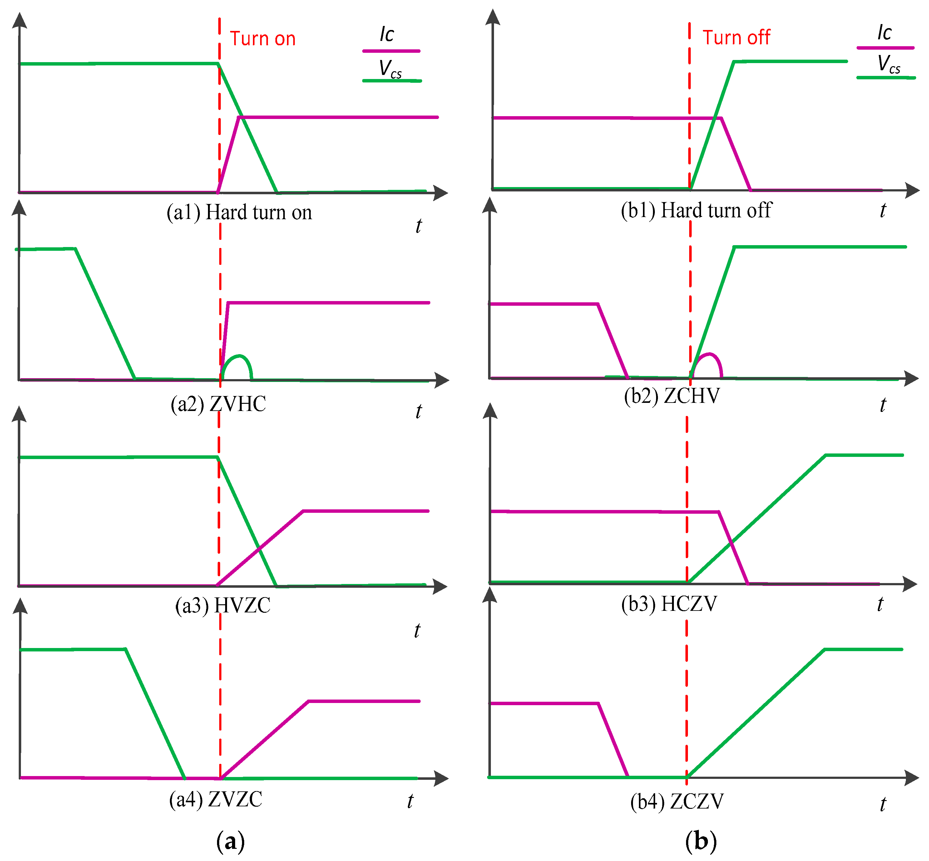
In hard switching, the IGBT voltage and current have a substantial overlap during the turn-on and turn-off events, resulting in large switching losses, as shown in Figure 1(a1,b1). To reduce the switching losses, the voltage and current waveforms can be manipulated in order to eliminate or minimize the overlap, which is the basic idea of soft switching. In the past, there are two typical soft switching types, which include zero-voltage switching and zero-current switching. Zero-voltage switching (ZVS) is defined as allowing the switching device to be turned on and off when the applied voltage across the device is effectively zero. Likewise, zero-current switching (ZCS) allows for the switching device to be turned off while the current conducted by the switching device is zero [2]. Also, a switching device, which is turned on under a zero-current switching condition, is also given in [9]. On the other hand, in recently, most of the papers specifically focus on the realization of ZVS condition for MOSFET and ZCS condition for IGBT based on the characteristics of the different switching device. ZVS is categorically used to describe the soft turn-on while ZCS is used to describe the soft turn-off. Both of these classifications are not very accurate for the IGBT device since the IGBT device dynamic loss depends on exactly how the voltage and current are applied, even if there is no ‘intended’ overlap. Detailed evaluation reveals that the classification must consider both the voltage transition and the current transient for both the turn-on and turn-off. A turn-on and turn-off switching classification are given in this paper, as shown in Figure 1. It is not only decided by if the voltage or current is zero before the switching device is turned on or off, but also take the states of the rising or falling edges of voltage and current into consideration. The turn-on and turn-off waveforms under hard switching condition are shown in Figure 1(a1,b1). The overlaps of voltage and current can be found in these switching transitions that cause the switching loss.
To reduce the switching loss, various gate driver circuits, additional passive snubber, and active auxiliary circuits are proposed. For example, in Figure 1(a2), the turn-on is named ZVHC turn-on since the voltage is reduced to zero before a hard imposed current rise (current rises with a high dI/dt). Similarly, Figure 1(b2) is named ZCHV turn-off since the current is reduced to zero before a high dV/dt applied to the IGBT. In the ZVHC turn-on, the high dI/dt generates a voltage bump, so there is some additional overlapping; hence, the turn-on loss is not zero. The voltage bump is caused by the bipolar IGBT physics since conductivity modulation needs time and current to establish. Similarly, in the ZCHV turn-off, the high dV/dt generates a current bump because stored carriers need time to recombine. In the case of ZCHV turn-off, the delay time between the ZC edge and the HV edge is critical in determining the current bump. In the case of the ZVHC case, the delay between the two edges (ZV and HC) does not affect the voltage bump since the delay does not help the establishment of the conductivity modulation. The voltage bump is strongly related to the applied dI/dt. With the help of the snubber circuit, the current rise during turn-on transition period and the voltage rise during turn-off transition period can slow down. As shown in Figure 1(a3), the current rise edge is softer than hard switching’s. It is defined as Hard Voltage Zero Current (HVZC) turn-on, which also indicates effective loss reduction. Similarly, Figure 1(b3) is defined as Hard Current Zero Voltage (HCZV) turn-off because of the soft voltage rise edge [9]. In Figure 1(a4), Zero Voltage Zero Current (ZVZC) turn-on is obtained since the voltage decreases to zero before the switching device is turned on, while the current also rises slowly [24]. In Figure 1(b4), ZCZV turn-off is achieved since the current decreases to zero before the switching device is turned off, while the voltage also rises slowly.
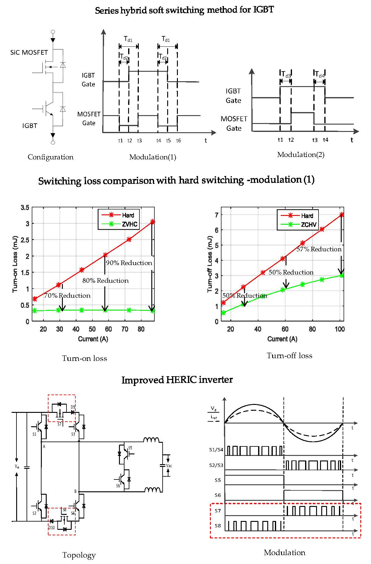
The ZVHC turn-on and ZCHV turn-off are frequently encountered in soft switching IGBT converters. Recently, such soft switching schemes are also proposed and are elegantly realized in a Si-SiC hybrid power switch. In this paper, a hybrid switching method is proposed to reduce the dynamic switching loss of IGBT. As shown Figure 2a, the SiC MOSFET is in series with the Si IGBT. The SiC MOSFET always keeps the off state during the IGBT switching-on or off transiation, as shown in Figure 2b. As a result, the IGBT can be turned on under ZVHC condition and turned off under ZCHV condition.
3. Hybrid Soft Switching Method Based on Device Level
3.1. Proposed Hybrid Switches Configuration and Modulation
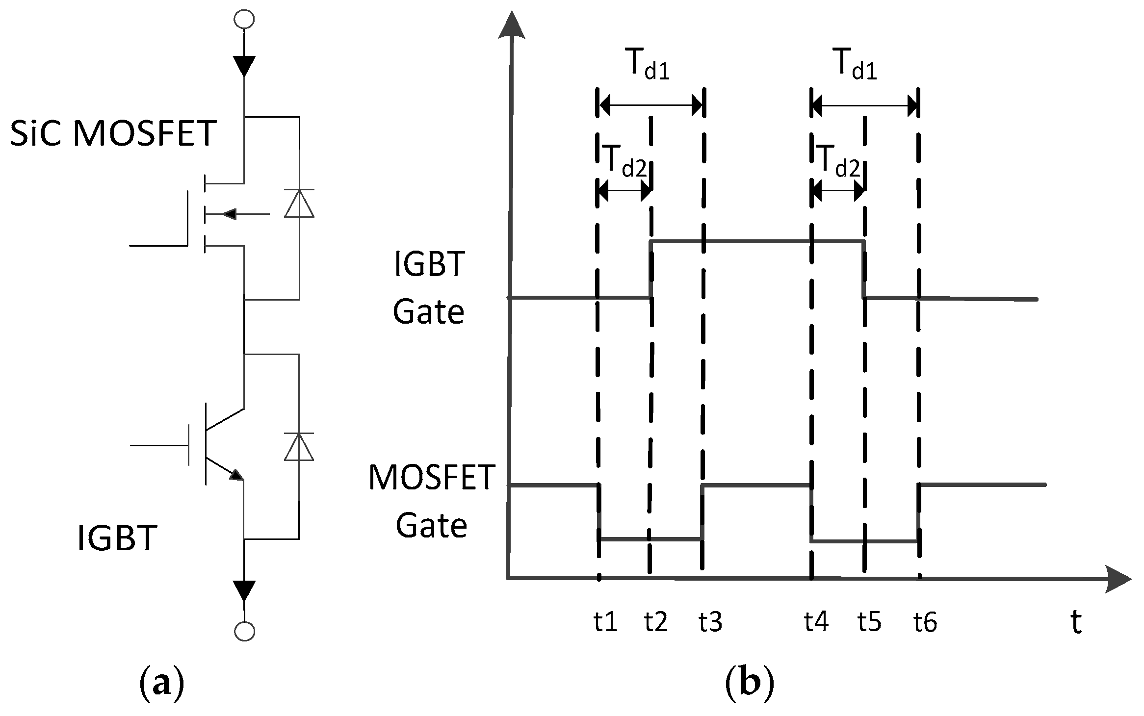
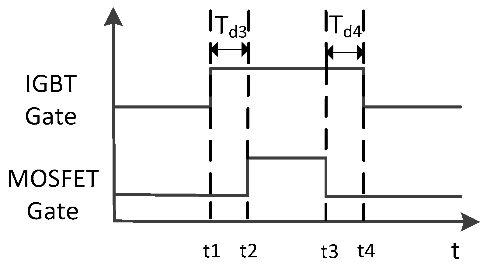
Figure 2 shows the series hybrid switches configuration and modulation. A SiC MOSFET is series with an IGBT, as displayed in Figure 2a. Providing SiC MOSFET a proper turn-off signal is the central concept to help IGBT achieve soft switching. In the turn-on period (t1~t3), at first, the voltage on the IGBT decreases to zero when the SiC MOSFET is turned off at t1. After a while, the IGBT is turned on at t2, which indicates that there will be no voltage and current crossing in theory. After the transient turn-on period of IGBT is finished, the SiC MOSFET is turned on again at t3. Then, the turn-on period of the hybrid switches is completed. In the turn-off period (t4~t6), at first, the current through IGBT decreases to when zero the SiC MOSFET is turned off at t4. After a while, the IGBT is turned off at t5, which indicates that there will be no voltage and current crossing in theory. After the transient turn-off period of IGBT is finished, the SiC MOSFET is turned on again at t6. Then, the turn-off period of the hybrid switches is completed. The dead time Td1 and delay time Td2, which have a significant effect on the switching loss, need to be carefully designed. To verify the proposed hybrid switching method, the series hybrid switches are applied to a common circuit-double pulse test, which is presented in the following sections.
3.2. Hybrid Soft Switching Method Analysis in Double Pulse Test
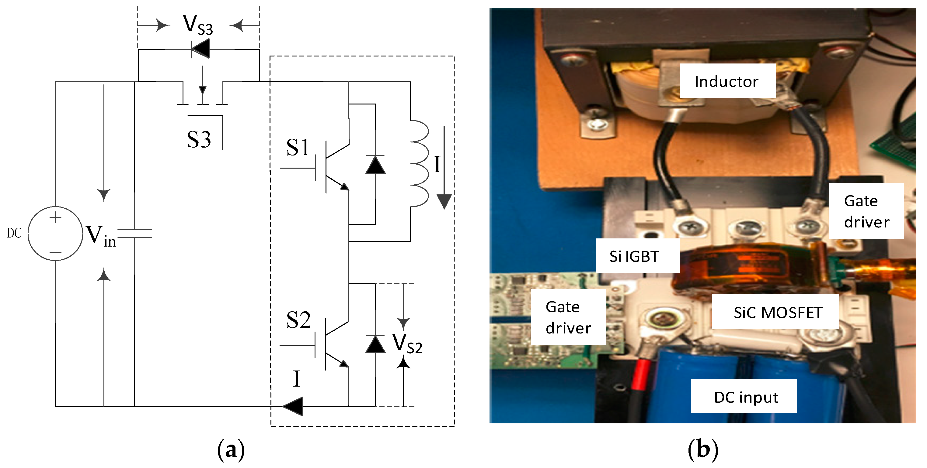
The common double pulse test circuit is given in the dashed box in Figure 3a. When testing the performance of switch S2, S1 is turned off all the time and is paralleled with an inductor. The double pulse drive signal is given to S2. By analyzing the voltage Vce and the current Ice of S2 in the whole switching period, Information, such as collector-emitter overvoltage, the reverse recovery current of diode, and switching loss can be found. As the overlap of switch’s voltage and current decide the switching loss, this paper provides a way to minimize such loss in order to achieve a better performance of IGBT. Figure 3a shows a new hybrid switches double-pulse testing circuit. S3 is a silicon carbide MOSFET connected in series with the primary circuit. S1 is turned off all the time. When S2 is about to be turned on or off, S3 will be turned off first and last for a specific time. After the switching transition of S2 is finished, S3 will be turned on again, as shown in Figure 2b. When the S3 is turned off, the current that is passed through S2 is forced to zero. The voltage and current states of three switches are different from the conventional one. There are six stages in switching-on or off period.
3.2.1. Turn-On Period
According to the proposed gate signals for the hybrid switches, which is shown in Figure 2b, there are six stages for the IGBT turn-on period t1~t3. Stage 1—before t1: S1 and S2 are off-state, while S3 is on-state. At this time, the voltage of S2 VS2 equals to input voltage Vin. Current of S2 Is2 and S3 Is3 are zero, while the current of S1 Is1 equals to the negative current of inductor IL; Stage 2—at t1: S3 is turned off at time t1. There is no voltage transfer in the circuit. The voltage will stay on S2. The current states of all the switches do not change too; Stage 3—t1~t2: during this time, the states of current and the voltage on each switch still keep unchanged; Stage 4—at t2: Figure 4a illustrates the equivalent circuit of hybrid switches double-pulse test at t2 in the switching-on period. As soon as S2 is turned on, the voltage of S2 transfers to the voltage of S3 VS3, which means that VS3 equals to Vin now. Red arrows show the current of each switch. S3’s capacitor is charged by the DC source. The current of inductor IL flows to the parallel diode. The S2’s capacitor voltage is discharged by itself. S3’s capacitor will stop charge until VS3 equals to Vin. Stage 5—t2~t3: during this time, the states of current and the voltage on each switch still keep unchanged; Stage 6—at t3: Figure 4b shows the equivalent circuit of hybrid switches double-pulse test at t3 in the switching-on period. As soon as S3 is turned on again, IL and S1’s diode reverse recovery current flow to S2. It brings the overcurrent of Is3 as a consequent. The S3’s capacitor voltage is discharged by itself. The voltage on the inductor equals to Vin; then, the whole switching-on period is finished.
3.2.2. Turn-Off Period
According to the proposed gate signals for the hybrid switches, which is shown in Figure 2b, there are also six stages for the IGBT turn-off period t4~t6. Stage 1—before t4: Before t4, S2 and S3 are on-state, while S1 is off-state. At this time, the voltage of S1 equals to input voltage Vin. Is2 and Is3 equal to IL; Stage 2—at t4: S3 is turned off at time t4. The equivalent circuit of hybrid switches double-pulse test at t4 in switching-off period is shown in Figure 5a. S3’s capacitor is charged by the DC source until VS3 equals to Vin. IL flows to the parallel diode of S2, while Is2 falls to zero; Stage 3—t4~t5, Stage 4—at t5, Stage 5—t5~t6: during this time, the states of current and the voltage on each switch still keep unchanged until S3 is turned on again. Stage 6—at t6: Figure 5b gives the equivalent circuit of hybrid switches double-pulse test at t6 in the switching-off period. At time t6, S3 is turned on. The S3’s capacitor voltage is discharged by itself until S3’s voltage falls to zero. Both the inductor current and the S1’s reverse recovery current flow to S2. S2’s capacitor voltage is charged until VS2 equals to Vin. Then, the whole switching-off period is finished. The current of S2 Is2 and S3 Is3 fall to zero, while the freewheeling current of inductor flows to anti-parallel diode gain.
3.3. Simulation and Experimental Results
3.3.1. Simulation Results
The simulations are carried out by using MATLAB/Simulink software (R2015a) to analyze and to initially verify the theoretical analysis. The parameters are used in the simulation are given in Table 1. Parasitic parameters are also considered for the devices. Input voltage Vin = 400 V, Td1 = 2 us, Td2 = 1 us. In the switching-on period, the voltage and current states keep the same in the stages 1, 2, 3. During this time, VS2 = Vin, IS2 = 0, VS3 = 0, as shown in Figure 6a. S2 is turned on at t2. The switching state becomes to S1S2S3 = 010. The voltage on S2 drops to zero, while the capacitor of S3 is charged to Vin. S3 is turned on again at t3. The switching state changes to S1S2S3 = 011. The voltage on S3 is discharged to zero. The current flows through S3, the inductor, and S2. The current rising edge of S2 can be observed at t3. The voltage and current waveforms of S2 and S3 in the switching-off period are shown in Figure 6b. S3 is turned off at t4. The switching state becomes to S1S2S3 = 010. The current of S2 falls to zero, while the capacitor of S3 is charged to Vin. The voltage and the current states keep the same in the stages 3, 4, 5. During this time, VS3 = Vin, IS2 = 0, VS2 = 0. S3 is turned on again at t6. The switching state changes to S1S2S3 = 001. The voltage on S3 drops to zero, while the capacitor of S2 is charged to Vin. Because of the impact of switches’ capacitor voltage change and parasitic inductor, there are current and voltage resonance happened in the circuit which can be observed at t2, t3, t4, and t6.
3.3.2. Experimental Results
- V-I Switching waveforms
For further verification, experimental results are also carried out. The parameters are listed in Table 1. Figure 7a,b shows the common double pulse test results for IGBT. Both in the turn-on and the turn-off period, there are overlaps between voltage and current waveforms, which cause switching losses-turn-on loss Eon and turn-off loss Eoff. It can be seen that IGBT operates under hard switching condition in the common double pulse test. IGBT module SKM100GB12T4 and SiC MOSFET module CAS120M12BM2 are adopted for the hybrid switches double-pulse experiment. Figure 3b shows the hardware test platform. In this test, Td2 is only 0.7 us, which can guarantee that the MOSFET turn-off transition is completed. Typical waveforms for the turn-on (87 A) and turn-off (102 A) during the test are shown in Figure 7c,d.
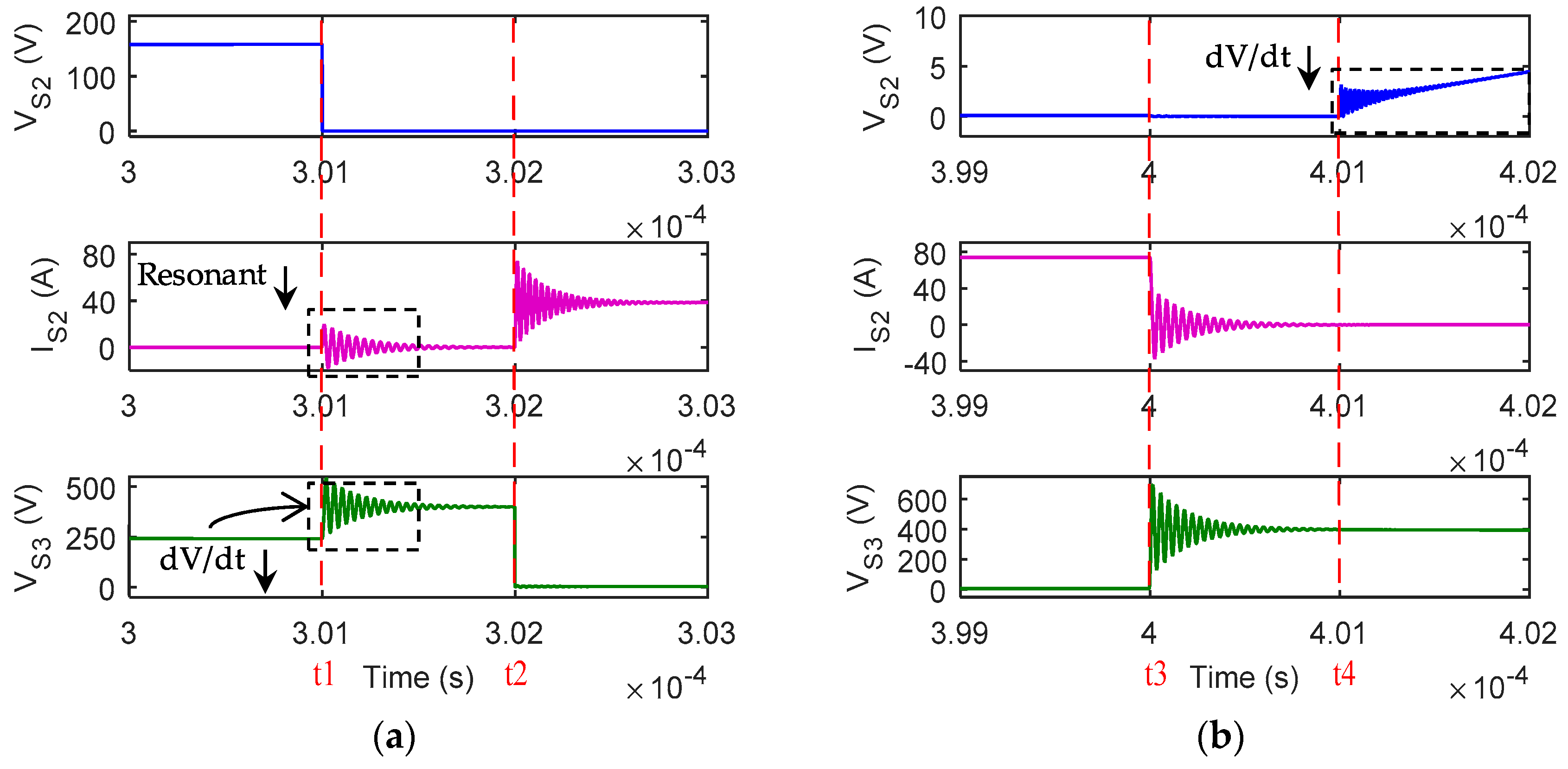
In the turn-on period, S3 is turned off at t1. The voltage of S2 is equal to the input voltage. After S3 finished its turn-off period, the S2 will be turned on at t2. As shown in Figure 7c, the voltage of S2 drops to zero. The capacitor of S3 will be charged by the DC source. Due to the impact of switches’ capacitor voltage change and the parasitic inductor, there is resonance that happened in the circuit. It can be observed a resonant current go through S2, which occurred in the dynamic period. S3 is turned on again at t3. The capacitor of S3 will be discharged to zero, while the voltage S1 equals to Vin. Because the freewheeling diode of S1 stops to conduct, the freewheeling current will directly go to S2. In addition, the reverse recovery current of the diode also flows to S2 which leads overshoot of the IGBT current at t3. Meanwhile, a small bump appears in IGBT voltage curve. It is caused by the bipolar IGBT physics since conductivity modulation needs time and current to establish. With the voltage bump that is generated by high dI/dt, there is some additional overlapping; hence, the turn-on loss is not zero. After the current is stable to the set value, the turn-on transition of the hybrid switches is finished. With the help of SiC MOSFET, the turn-on behavior of the IGBT under this condition can be defined as ZVHC turn-on. However, it can be seen that there still have the switching-on loss of IGBT, which consists of the loss occur at t2 and t3.
In the turn-off period, S3 is turned off at t4, as shown in Figure 7d. The voltage of S3 rises to Vin. At the same time, the current of S2 drops to zero. As aforementioned, there is also current resonance happened during the dynamic period. After S3 finished its turn-off period, the S2 will be turned off at t5. The current and voltage states on each switch keep unchanged. After 1.3 us, S3 is turned on again. The overshoot of voltage can be observed caused by the stray inductance in the circuit. It is higher than hard-switching’s, because of the high di/dt that is caused by the SiC MOSFET fast switching-on speed. With the high dV/dt happens on S2, a current bump is found because the stored carriers still need more time to recombine. The current bump brings the overlapping of current and voltage, which causes additional switching-off loss. It is the main reason that the switching-off loss is not zero as theoretical analysis. When the voltage S2 is equal to the DC input voltage, the turn-off transition of the hybrid switches is finished. There also have two parts of switching-off loss of IGBT that occur at t4 and t6. With the help of SiC MOSFET, the turn-off behavior of the IGBT can be defined as ZCHV turn-off.
- 2.
- Switching loss comparison
According to the new V-I curves of IGBT in the hybrid switches, the overlap of current and the voltage in turn-on period and turn-off period are much smaller when compared to the hard switching’s. The IGBT’s dynamic switching loss is efficiently reduced since it is the integration of voltage and current of the overlap [25]. As shown in Figure 7c,d, there are two parts of IGBT switching loss happened both during the turn-on and turn-off period. In this section, the common double pulse test experimental results also are carried out. The same type of IGBT is introduced in the test to get the switching loss under hard switching condition. As shown in Figure 8, the comparison results of switching loss under hard switching and soft switching at a different level of current are given in both the turn-on and turn-off period. In the turn-on period, the current is varies in the range of 0~90 A. As shown in Figure 8a, the red line is the switching-on loss under hard switching condition, while the green line is the switching-on loss under ZVHC turn-on condition. It can be seen that there still has a small switching-on loss for IGBT under ZVHC turn-on condition because of the voltage bump. However, at 87 A, more than 90% IGBT turn-on dynamic loss is reduced with the help of SiC MOSFET. During the turn-off period, the current varies in the range of 0~102 A. As shown in Figure 8b, at 102 A, only 57% turn-off loss is reduced in the turn-off period. There still has a considerable switching-off loss for IGBT under the ZCHV turn-off condition because of the current bump. Further study about the current bump is given in the following section.
- 3.
- Parameters design
There are two critical parameters in the design of SiC MOSFET gate signal, which are the dead time Td1 and the delay time Td2. For the design of the delay time Td2, the primary concern is making sure that the turn-off transition of SiC MOSFET is completed during this time. It can keep the whole circuit from the overlap of the SiC MOSFET switching transition time and the IGBT switching transition time. As mentioned previously, there is voltage bump in the IGBT’s turn-on period since the conductivity modulation needs more time and current to establish, while there is a current bump in the IGBT’s turn-off period because stored carriers need more time to recombine. As a result, the states of the voltage bump and the current bump are decided by the times of t2~t3 and t5~t6. When Td2 is fixed, the dead time Td1 becomes the critical factor that affects the voltage and the current bumps. Moreover, the switching losses of IGBT will also change with different Td1.
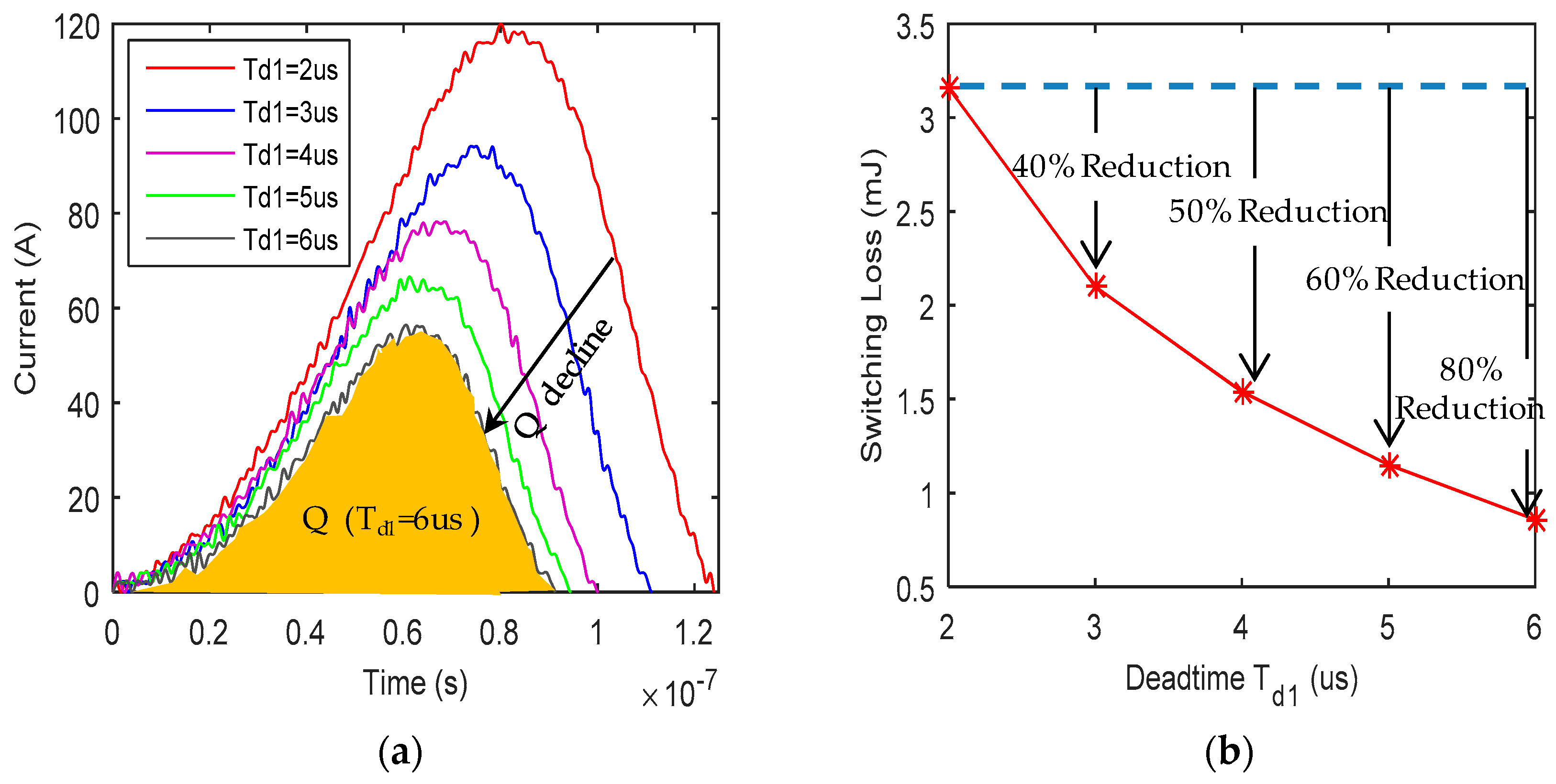
As shown in Figure 7d, there is considerable a current bump, which is the main reason for the significant switching-off loss under ZCHV turn-off condition. In order to reduce the switching-off loss, the relationship between the current bump, and the dead time Td1 is studied in this section. When the Td2 is fixed to 0.7 us, the turn-off current bumps of IGBT with various Td1 are shown in Figure 9a. It can be seen that the current bump is getting smaller with the increase of Td1. As the charge Q is the time integral of current, the Q is relatively decreased with a smaller current bump. As a result, the switching-off loss is also reduced, which is shown in Figure 9b. When the dead time increases to 6 us, 80% IGBT dynamic turn-off loss is decreased. Moreover, the voltage overshoot of IGBT can be also improved. However, the dead time also has an influence on the effective duty cycle for the switch. With a larger dead time, the distortion of output waveform will be more serious when the hybrid switches apply to the practical circuit. As a result, there is a trade-off between the switching loss and the duty loss for the design of the dead time. Moreover, with the application of different IGBT, the state of the current bump will be different too. As shown in Figure 10, Another MG300J2YS50 IGBT is also tested. Unlike Figure 9a, the relationship between Td1 and the current bump is also changed. The current bump can be cut down significantly by choosing the value of Td1 as 3 us instead of 2 us. However, there is barely reduction of the current bump when Td1 is longer than 4 us. In order to achieve the best design of Td1 with the consideration of distortion and switching loss reduction, the current bump state of IGBT is also essential to study.
4. Optimization and Application
4.1. Improved Modulation for the Hybrid Switches
4.1.1. Improved Modulation
With the help of the hybrid switching method, the IGBT dynamic switching is reduced significantly. However, there’s still has considerable switching loss, especially the switching-off loss. To improve the performance of the hybrid switches, an improved modulation method is also proposed. As shown in Figure 11, the IGBT is turned on at t1. Then, the MOSFET is turned on at t2. The delay time between t1 and t2 is Td3. At t3, the MOSFET is turned off first. After another delay time Td4, the IGBT is turned off at t4. Instead of high dV/dt that happened on the IGBT, the IGBT will have low dV/dt by sharing the input voltage with the MOSFET naturally. ZCZV turn-off can be realized, as shown in Figure 1 (b4).
4.1.2. Simulation Results
Simulation results of the hybrid switches with the improved modulation for the double test are carried out, as shown in Figure 12. The parameters are used in the simulation are given in Table 1. Input voltage Vin = 400 V, Td3 = 1 us, Td4 = 1 us. In the turn-on period, both S2 (IGBT) and S3 (MOSFET) are off-state before t1. The current of S2 IS2 is zero. The input voltage is shared by these two switches. The S2 is turned on at t1, as shown in Figure 12a. The voltage on the IGBT drops to zero, while the voltage on the S3 increases to the input voltage. With the smaller dV/dt, it can be seen that the resonant happened in the circuit is much smaller when compared to Figure 6a. After a delay time Td3, S3 is turned on. A high di/dt still can be observed. Figure 12b gives the V-I waveforms of the turn-off transition period. S3 is turned off at t3. IS2 falls to zero, while the voltage on S3 VS3 increases to 400 V. Because of the high dV/dt, there is still a resonant that happened in the circuit. When S2 is turned off at t4, the voltage of S2 VS2 starts to increase slowly to share the input the input voltage with S3. Since there is low dV/dt that is applied to the IGBT when compared to Figure 6b, Figure 12b is defined as ZCZV (Zero Current Zero Voltage) turn-off. The resonant is eliminated effectively due to the small dV/dt on S2. Moreover, the stored carriers of IGBT have more time to recombine with the small dV/dt, which helps to reduce the current bump. As a result, the dynamic turn-off loss of IGBT can be reduced effectively under the ZCZV turn-off condition. In addition, the MOSFET is switched on or off for one time in the improved modulation. It helps simplify the design and implement of the gate signal of MOSFET. For the design of the delay time, the main consideration of Td3 is still a trade-off between voltage bump and distortion. Unlike Td3, Td4 only need to make sure the switching-off transition of MOSFET is finished in this time. In conclusion, better performance of IGBT can be achieved with the improved modulation in the hybrid switches. Further application circuit of the hybrid switches is given in the next section.
4.2. Hybrid Switching Method Apply to HERIC Inverter
4.2.1. Configuration and Modulation
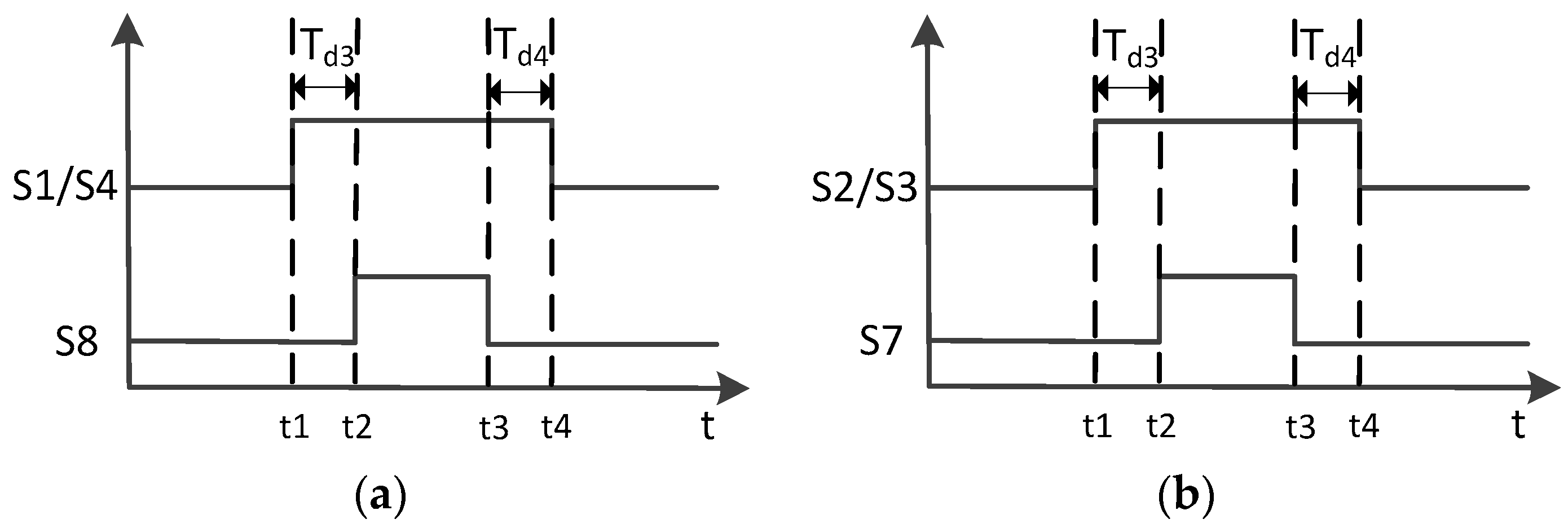
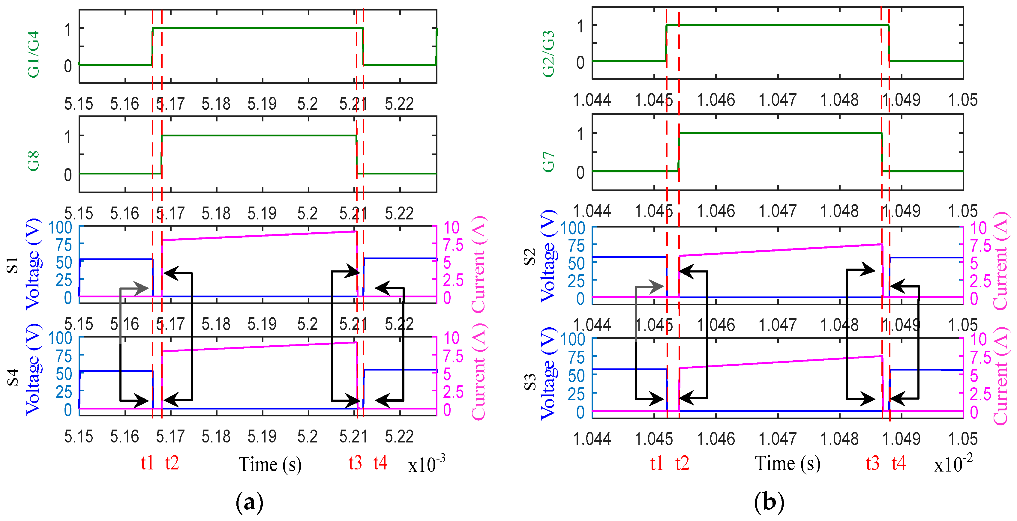
In the previous sections, with the help of SiC MOSFET, the dynamic loss IGBT is efficiently reduced. This hybrid switching method also can be applied to a practical circuit. As shown in Figure 13, an improved HREIC inverter is proposed with the application of the hybrid switches. Two SiC MOSFETs and two diodes are added to the common HERIC circuit, as shown in Figure 13a. The additional diodes are introduced to prevent the IGBT S1/S2 from current freewheeling. The improved modulation for the new HERIC inverter is given in the Figure 13b. The modulation of switches S1~S5 keep the same as the conventional one, while the gate signals for the MOSFET are designed according to the improved hybrid switches modulation. The gate signals detail in the positive and negative cycle is given in Figure 14.
In the positive cycle, S2, S3, S6, and S7 are off-state, while S5 is turned on. S1, S4, and S8 operate at high frequency. As shown in Figure 14a, S14S8 = 000 before t1. The freewheeling current goes through the anti-paralleled diode of S6 and S5. S1 and S4 are turned on at t1. The voltage on S1 and S4 are discharged to zero by themselves. By adopting the D9, the freewheeling current goes to S1 is blocked. There is no current flow to S4 either because S8 is turned off at this time. In conclusion, the freewheeling current path keeps the same before t2. S8 is turned on at t2. The currents of S1 and S4 start to increase. The inverter operates in the active mode, which means that the current flows through S1, ac side, S4, S8, and D10. The output voltage VAB is equal to the input voltage. As the turn-on transition is finished, it can be achieved that there is a gap between the voltage falling edge and the current rising edge of IGBT. As a result, the dynamic turn-on losses of S1 and S4 can cut down. At t3, S8 is turned off first. The currents of S1 and S4 fall to zero, while the freewheeling current flows to the anti-paralleled diode of S6 and S5 again. The voltages of S1 and S4 start to increase when S1 and S4 are turned off at t4. There is also a gap between the current falling edge and the voltage rising edge of IGBT, which will help to reduce the dynamic turn-off losses of S1 and S4. The gate signals in the negative cycle are shown in the Figure 14b. With the same operation principle, S7 is also able to help IGBT S2 and S4 cut down the dynamic switching loss in the negative cycle.
4.2.2. Simulation Results
With the proposed modulation, the output voltage of the improved HERIC inverter is perfect 240 V/60 Hz sinusoidal wave. The improved inverter works as a regular of the common HERIC inverter. Figure 15 shows the simulated waveforms of the proposed HERIC inverter in the positive and negative cycle. In the positive cycle, the gate signals of S1, S4, and S8 are given in Figure 15a. The voltages of S1 and S4 drop to zero when S1 and S4 are turned on at t1. Since the freewheeling current is blocked by D9, the currents of S1 and S4 keep at zero until S8 is turned on. At t2, S8 is turned on. There is a current path that is composed by S1, ac side, S4, D10, and S8. The current goes through S1 and S4 start to increase then. As the switching-on transition is finished, a ZVHC turn-on is realized for the IGBT. S8 is turned off first at t3. The current goes through S1 and S4 drops to zero again, while the voltages of S1 and S4 keep at zero since S1 and S4 are still turned on at this time. At t4, S1 and S4 are turned off. The voltages of S1 and S4 start to increase. As the switching-off transition is finished, a ZCZV turn-off is realized for the IGBT. As shown in Figure 15b, the ZVHC turn-on and the ZCZV turn-off are also achieved for IGBT S2 and S3 with the help of S7 and D10 in the negative cycle. As a result, the dynamic switching losses of the high-frequency switch IGBT S1~S4 can be efficiently reduced. With smaller thermal stress coming from switching loss, IGBTs in the inverter can push to operate at the higher switching frequency.
5. Conclusions
This paper presents a novel series hybrid switching method to achieve IGBT’s dynamic switching loss reduction by switching under Zero Voltage Hard Current (ZVHC) turn-on and Zero Current Hard Voltage (ZCHV) turn-off conditions. A SiC MOSFET is utilized to generate a dead time in order to help IGBT avoiding voltage and current crossing during the switching transition periods. Theoretically, the IGBT switching loss is zero, but the stored minority charge will have an impact on the actual loss. 90% turn-on loss reduction and 57% turn-off loss reduction still can be achieved in theexperimental results. In addition, the hybrid switching method can be easily applied to the voltage source converters. The modulation for SiC MOSFET is easy to design because it is only decided by the gate signal of the series IGBT. With the improved modulation strategy, only one SiC MOSFET and a diode can help two high-frequency switches to reduce the dynamic switching loss in the improved HERIC inverter. The cost can be cut down significantly when compared with the parallel hybrid switch. However, there still have considerable switching-off loss that is caused by the current bump with the proposed method. It still needs improvement for the hybrid switching method. To reduce the current bump efficiently, the approach by using the lifetime killer or decreasing the voltage rise ratio (dv/dt) can be further studied. Moreover, although the SiC MOSFET can help IGBT to reduce the stress of high switching loss, the conduction loss of the hybrid switches is increased because of the series SiC MOSFET. To improve the efficiency of the hybrid switching method, more research needs to be done for the further application in the future.
Author Contributions
Lan Ma and Alex Q. Huang proposed the hybrid soft switching method for IGBT; Hongbing Xu and Jianxiao Zou built the simulation model; Lan Ma and Alex Q. Huang performed the experiments for the hybrid soft switching method; Lan Ma and Hongbing Xu analyzed the simulation and experimental results; Lan Ma and Kai Li wrote the paper.
Conflicts of Interest
The authors declare no conflict of interest.
References
- Velander, E.; Kruse, L.; Wiik, T.L.; Wiberg, A.; Colmenares, J.; Nee, H.P. An IGBT Turn-ON Concept Offering Low Losses Under Motor Drive dv/dt Constraints Based on Diode Current Adaption. IEEE Trans. Power Electron. 2017, 99, 1143–1153. [Google Scholar] [CrossRef]
- Chen, K.; Stuart, T.A. A study of IGBT turn-off behavior and switching losses for zero-voltage and zero-current switching. In Proceedings of the Applied Power Electronics Conference and Exposition, Boston, MA, USA, 23–27 February 1992; pp. 411–418. [Google Scholar]
- Hochberg, M.; Sack, M.; Mueller, G. Simple Gate-boosting Circuit for Reduced Switching Losses in Single IGBT Devices. In Proceedings of the International Exhibition and Conference for Power Electronics, Intelligent Motion, Renewable Energy, and Energy Management, PCIM-Europe, Nuremberg, Germany, 10–12 May 2016; pp. 1–6. [Google Scholar]
- John, V.; Suh, B.S.; Lipo, T.A. High-performance active gate drive for high power IGBTs. IEEE Trans. Ind. Appl. 1999, 2, 1519–1529. [Google Scholar]
- Sun, Y.; Sun, L.; Esmaeli, A.; Zhao, K. A Novel Three Stage Drive Circuit for IGBT. In Proceedings of the 2006 1ST IEEE Conference on Industrial Electronics and Applications, Singapore, 24–26 May 2006; pp. 1–6. [Google Scholar]
- Sokolov, A.; Mascarella, D.; Joos, G. Variable-speed IGBT gate driver with loss/overshoot balancing for switching loss reduction. In Proceedings of the 2014 IEEE Energy Conversion Congress and Exposition, Pittsburgh, PA, USA, 14–18 September 2014; pp. 1232–1239. [Google Scholar]
- Wang, Z.; Shi, X.; Tolbert, L.M.; Wang, F.F.; Blalock, B.J. A di/dt Feedback-Based Active Gate Driver for Smart Switching and Fast Overcurrent Protection of IGBT Modules. IEEE Trans. Power Electron. 2014, 29, 3720–3732. [Google Scholar] [CrossRef]
- Yang, X.; Long, Z.; Wen, Y.; Huang, H.; Palmer, P.R. Investigation of the trade-off between switching losses and EMI generation in Gaussian S-shaping for high-power IGBT switching transients by active voltage control. IET Power Electron. 2016, 9, 1979–1984. [Google Scholar] [CrossRef]
- Caponet, M.C.; Profumo, F.; Tenconi, A. Evaluation of power losses in power electronic converters for industrial applications: Comparison among hard switching, ZVS, and ZVS-ZCS converters. In Proceedings of the IEEEPower Conversion Conference, PCC-Osaka 2002, Osaka, Japan, 2–5 April 2002; pp. 1073–1077. [Google Scholar]
- Gautam, D.S.; Musavi, F.; Eberle, W.; Dunford, W.G. A zero voltage switching full-bridge DC-DC converter with capacitive output filter for a plug-in-hybrid electric vehicle battery charger. IEEE Trans. Appl. Power Electron. 2012, 28, 1381–1386. [Google Scholar]
- Choe, H.J.; Chung, Y.C.; Sung, C.H.; Yun, J.J.; Kang, B. Passive Snubber for Reducing Switching-Power Losses of an IGBT in a DC–DC Boost Converter. IEEE Trans. Power Electron. 2014, 29, 6332–6341. [Google Scholar] [CrossRef]
- Liu, F.; Yan, J.; Ruan, X. Zero-Voltage and Zero-Current-Switching PWM Combined Three-Level DC/DC Converter. IEEE Trans. Ind. Electron. 2010, 57, 1644–1654. [Google Scholar]
- Stein, C.D.; Hey, H.L. A true ZCZVT commutation cell for PWM converters. IEEE Trans. Power Electron. 2000, 15, 185–193. [Google Scholar] [CrossRef]
- Tarzamni, H.; Babaei, E.; Gharehkoushan, A.Z. A Full Soft-Switching ZVZCS Flyback Converter Using an Active Auxiliary Cell. IEEE Trans. Ind. Electron. 2017, 64, 1123–1129. [Google Scholar] [CrossRef]
- Ning, G.; Chen, W.; Shu, L.; Qu, X. A Hybrid ZVZCS Dual-Transformer-Based Full-Bridge Converter Operating in DCM for MVDC Grids. IEEE Trans. Ind. Electron. 2017, 32, 5162–5170. [Google Scholar] [CrossRef]
- Hoffmann, K.F.; Karst, J.P. High-frequency power switch—Improved performance by MOSFETs and IGBTs connected in parallel. In Proceedings of the European Conference on Power Electronics and Applications, Dresden, Germany, 11–14 September 2005. [Google Scholar]
- Lai, J.S.; Yu, W.; Sun, P.; Leslie, S.; Arnet, B.; Smith, C.; Cogan, A. A Hybrid-Switch-Based Soft-Switching Inverter for Ultrahigh-Efficiency Traction Motor Drives. IEEE Trans. Ind. Appl. 2012, 50, 1966–1973. [Google Scholar] [CrossRef]
- Sun, P.; Lai, J.S.; Liu, C.; Yu, W. A 55-kW Three-Phase Inverter Based on Hybrid-Switch Soft-Switching Modules for High-Temperature Hybrid Electric Vehicle Drive Application. IEEE Trans. Ind. Appl. 2012, 48, 962–969. [Google Scholar] [CrossRef]
- Ning, P.; Li, L.; Wen, X.; Cao, H. A Hybrid Si IGBT and SiC MOSFET Module Development. CES J. Mag. 2017, 1, 360–366. [Google Scholar]
- Rahimo, M.; Canales, F.; Minamisawa, R.A.; Papadopoulos, C.; Vemulapati, U.; Mihaila, A.; Kicin, S.; Drofenik, U. Characterization of a Silicon IGBT and Silicon Carbide MOSFET Cross-Switch Hybrid. IEEE Trans. Power Electron. 2015, 30, 4638–4642. [Google Scholar] [CrossRef]
- Song, X.; Huang, A.Q.; Lee, M.C.; Peng, C. High voltage Si/SiC hybrid switch: An ideal next step for SiC. In Proceedings of the 2015 IEEE 27th International Symposium on Power Semiconductor Devices & IC’s (ISPSD), Hong Kong, China, 10–14 May 2015; pp. 289–292. [Google Scholar]
- Minamisawa, R.A.; Vemulapati, U.; Mihaila, A.; Papadopoulos, C.; Rahimo, M. Current Sharing Behavior in Si IGBT and SiC MOSFET Cross-Switch Hybrid. IEEE Electron. Device Lett. 2016, 37, 1178–1180. [Google Scholar] [CrossRef]
- He, J.; Katebi, R.; Weise, N. A Current-Dependent Switching Strategy for Si/SiC Hybrid Switch Based Power Converters. IEEE Trans. Ind. Electron. 2017, 64, 8344–8352. [Google Scholar] [CrossRef]
- Dudrik, J.; Pástor, M.; Lacko, M.; Žatkovič, Z. Zero-Voltage and Zero-Current Switching PWM DC-DC Converter Using Controlled Secondary Rectifier with One Active Switch and Non-Dissipative Turn-Off Snubber. IEEE Trans. Power Electron. 2017, 33, 6012–6023. [Google Scholar] [CrossRef]
- Kai, L.; Zhao, J.C.; Wu, W.J.; Li, M.S.; Ma, L.; Zhang, G. Performance Analysis of Zero Common-Mode Voltage Pulse-Width Modulation Techniques for Three-Level Neutral Point Clamped Inverters. IET Power Electron. 2016, 9, 2654–2664. [Google Scholar] [CrossRef]
Figure 1.
Turn-on and turn-off switching classification (a) Turn-on; and, (b) Turn-off.

Figure 2.
(a) Proposed Hybrid Switches Configuration; and, (b) Modulation.

Figure 3.
Double Pulse Test (DPT) for the hybrid switches (a) DPT Circuit; and, (b) DPT platform.

Figure 4.
Turn-on period (a) Stage 4-at t2; and, (b) Stage 6-at t3.
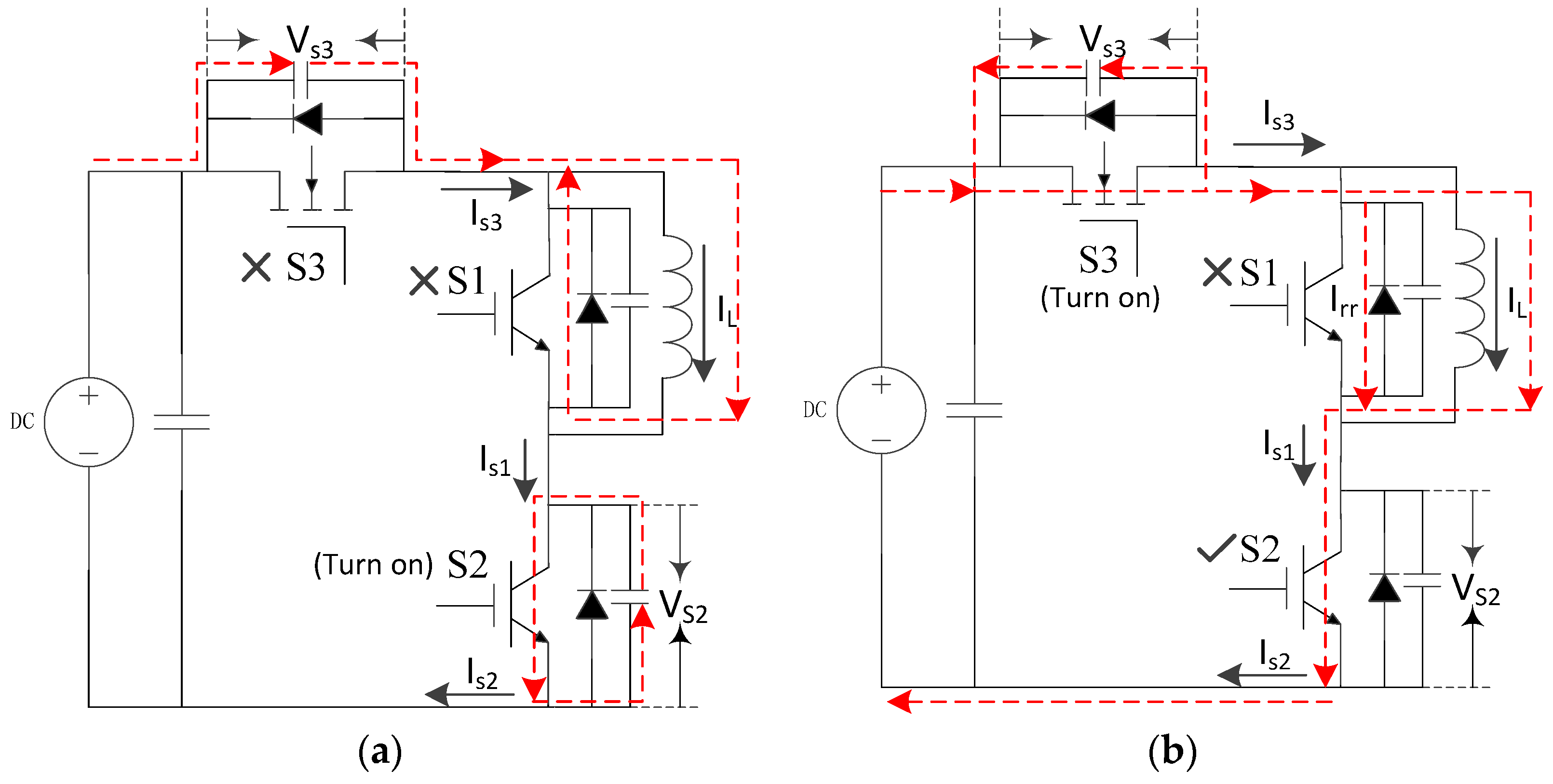
Figure 5.
Turn-off period (a) Stage 2-at t4; and, (b) Stage 6-at t6.
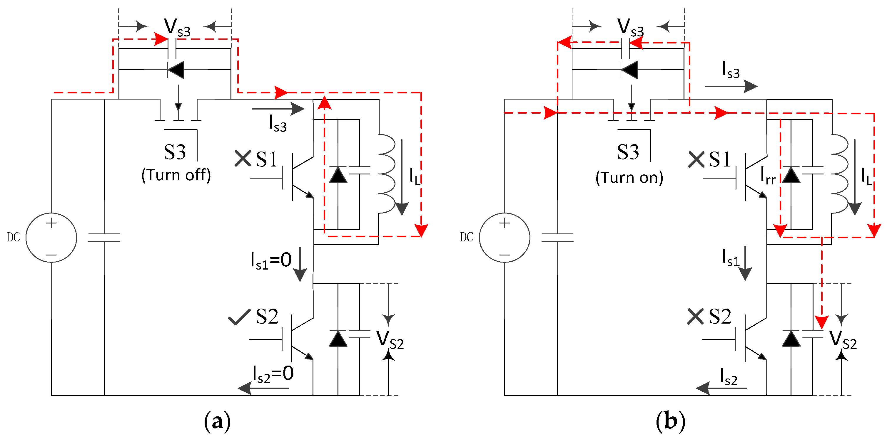
Figure 6.
Simulation results of double pulse test for the hybrid switches (Td1 = 2 us; Td2 = 1 us) (a) Turn-on; and, (b) Turn-off.
Figure 6.
Simulation results of double pulse test for the hybrid switches (Td1 = 2 us; Td2 = 1 us) (a) Turn-on; and, (b) Turn-off.
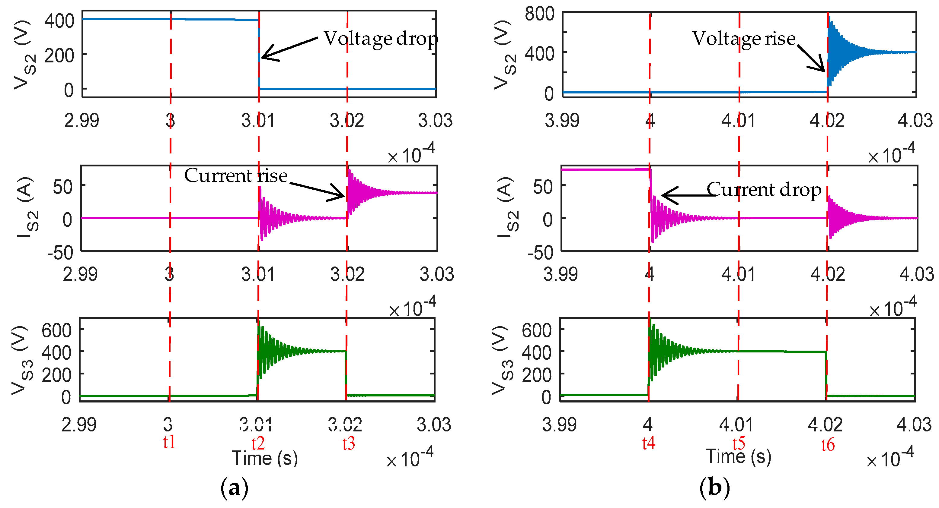
Figure 7.
Experimental comparison results of IGBT V-I curves in different double pulse test (a) IGBT turn-on transition in the common DPT; (b) IGBT turn-off transition in the common DPT; (c) IGBT turn-on transition in DPT with hybrid switches; and, (d) IGBT turn-off transition in DPT with hybrid switches.
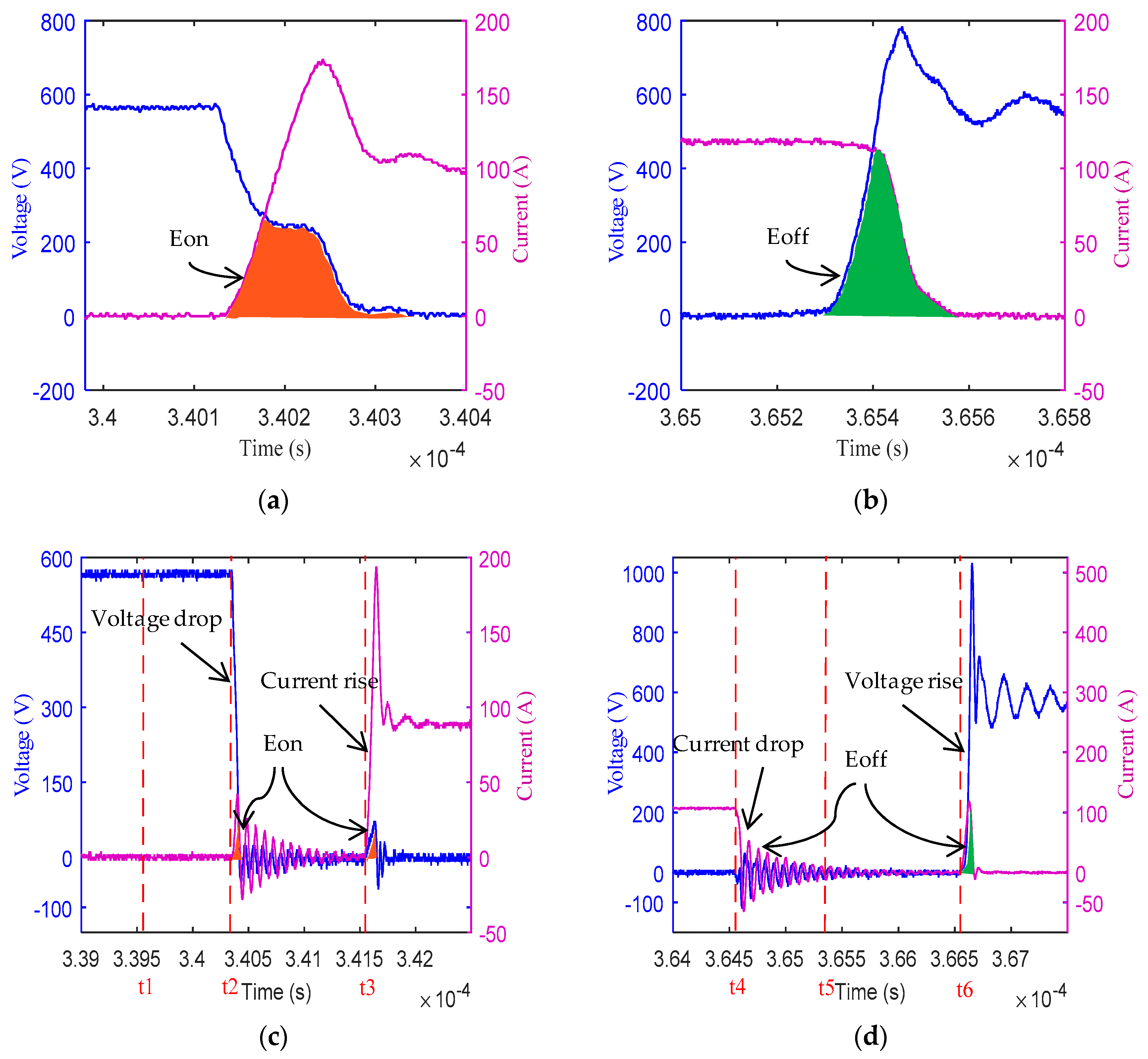
Figure 8.
IGBT switching losses comparison during on/off periods (a) Turn-on loss; and, (b) Turn-off loss.
Figure 8.
IGBT switching losses comparison during on/off periods (a) Turn-on loss; and, (b) Turn-off loss.
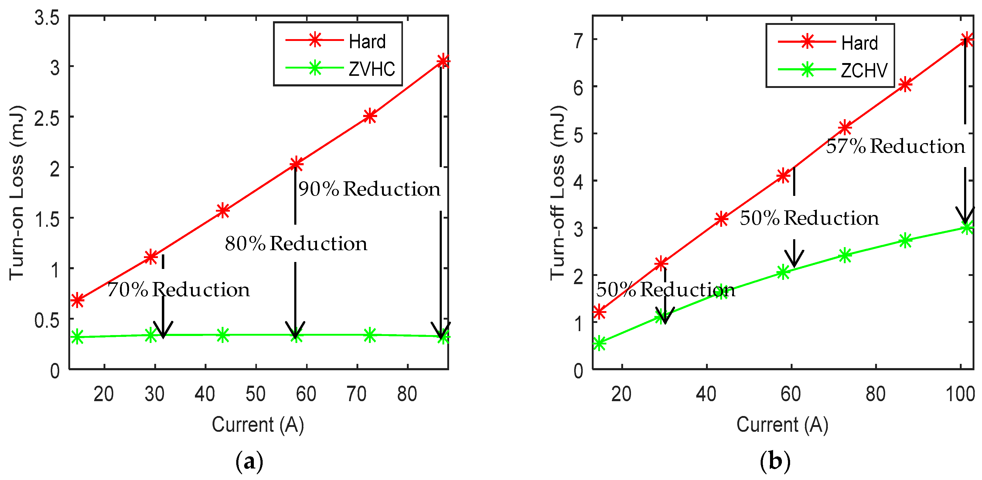
Figure 9.
IGBT ZCHV turn-off current bumps and the turn-off losses with various Td1 (a) ZCHV turn-off the current bumps in the IGBT with various Td1; and, (b) The IGBT ZCHV turn-off losses with various Td1.
Figure 9.
IGBT ZCHV turn-off current bumps and the turn-off losses with various Td1 (a) ZCHV turn-off the current bumps in the IGBT with various Td1; and, (b) The IGBT ZCHV turn-off losses with various Td1.

Figure 10.
(a) Hybrid switches DPT test platform with a different IGBT; and, (b) A different IGBT ZCHV turn-off current bumps with various Td1.
Figure 10.
(a) Hybrid switches DPT test platform with a different IGBT; and, (b) A different IGBT ZCHV turn-off current bumps with various Td1.
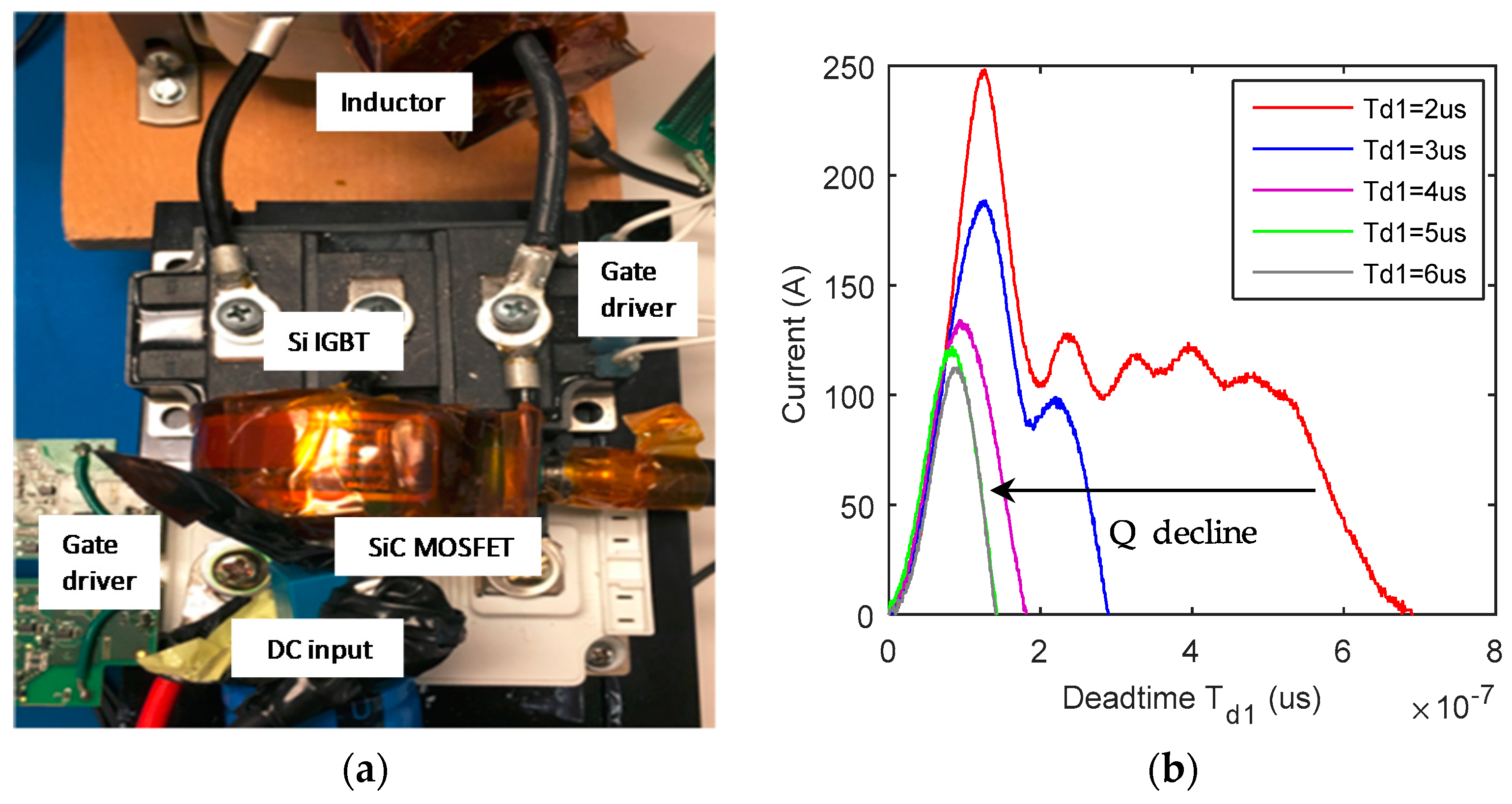
Figure 11.
Improved modulation for the hybrid switches.

Figure 12.
Simulation results of double pulse test for the hybrid switches with improved modulation (a) Zero Current Hard Voltage (ZCHC) turn-on; and, (b) Zero Current Zero Voltage (ZCZV) turn-off.
Figure 12.
Simulation results of double pulse test for the hybrid switches with improved modulation (a) Zero Current Hard Voltage (ZCHC) turn-on; and, (b) Zero Current Zero Voltage (ZCZV) turn-off.

Figure 13.
Improved HERIC inverter circuit and modulation with the hybrid switching method application (a) Improved HERIC inverter; (b) Improved modulation.
Figure 13.
Improved HERIC inverter circuit and modulation with the hybrid switching method application (a) Improved HERIC inverter; (b) Improved modulation.
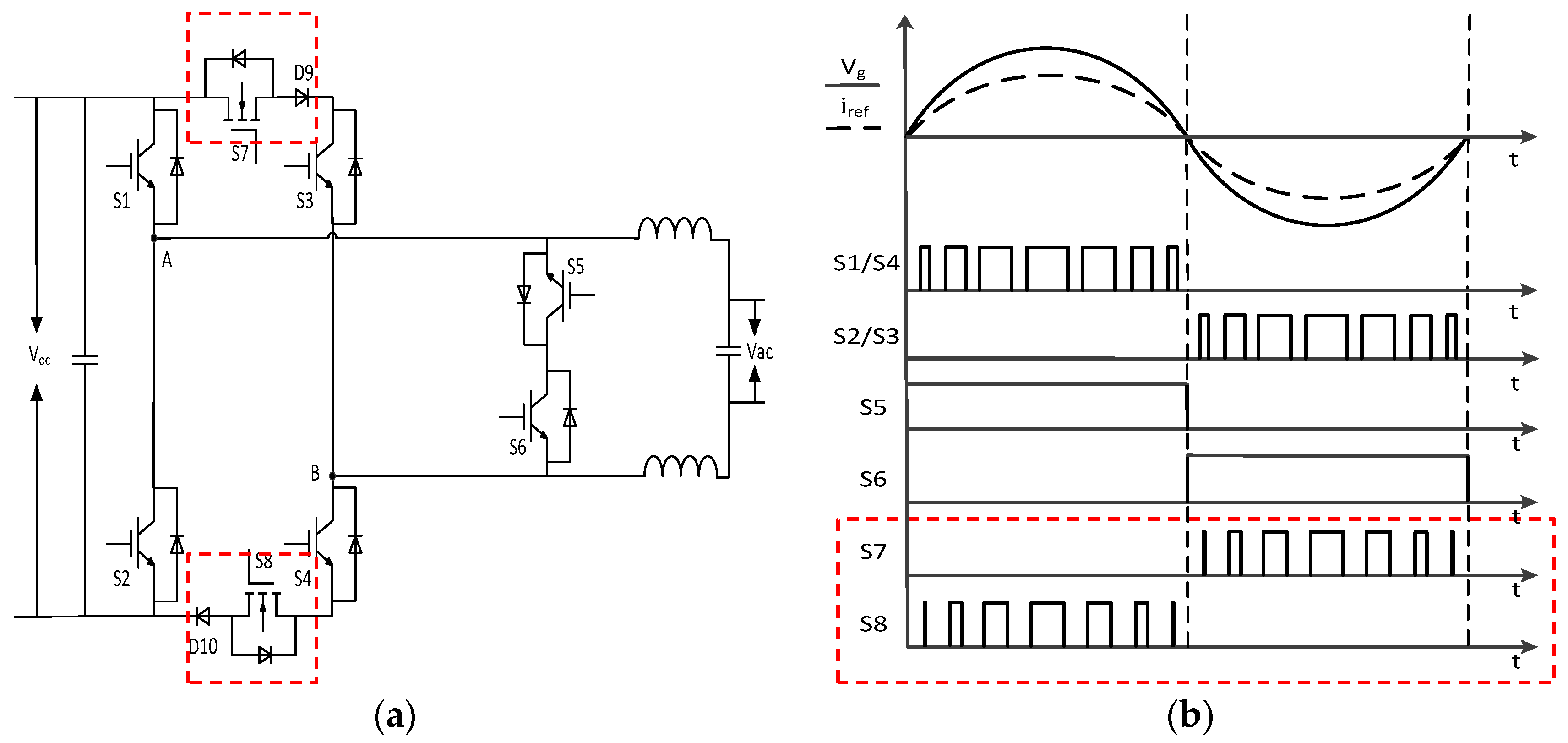
Figure 14.
Gate signals of IGBT and MOSFET (a) The positive cycle; and, (b) The negative cycle.

Figure 15.
Simulation results of the improved HERIC inverter (a) The positive cycle; (b) The negative cycle.
Figure 15.
Simulation results of the improved HERIC inverter (a) The positive cycle; (b) The negative cycle.


Table 1.
The double pulse test for the hybrid switches parameters.
| Parameter | Value | Parameter | Value |
|---|---|---|---|
| Input voltage | 400/580 V | Inductor | 1 mH |
| Td1 | 2 us | Td2 | 1/0.7 us |
| Si IGBT Gate Resistor | R = 1 Ω | SiC MOSFET Gate Resistor | Ron = 5 Ω/Roff = 2.5 Ω |
| Si IGBT | SKM100GB12T4 1.2 KV/100 A | SiC MOSFET | CAS120M12BM2 1.2 kV/120 A |
© 2018 by the authors. Licensee MDPI, Basel, Switzerland. This article is an open access article distributed under the terms and conditions of the Creative Commons Attribution (CC BY) license (http://creativecommons.org/licenses/by/4.0/).
Share and Cite
MDPI and ACS Style
Ma, L.; Xu, H.; Huang, A.Q.; Zou, J.; Li, K. IGBT Dynamic Loss Reduction through Device Level Soft Switching. Energies 2018, 11, 1182. https://doi.org/10.3390/en11051182
AMA Style
Ma L, Xu H, Huang AQ, Zou J, Li K. IGBT Dynamic Loss Reduction through Device Level Soft Switching. Energies. 2018; 11(5):1182. https://doi.org/10.3390/en11051182
Chicago/Turabian StyleMa, Lan, Hongbing Xu, Alex Q. Huang, Jianxiao Zou, and Kai Li. 2018. "IGBT Dynamic Loss Reduction through Device Level Soft Switching" Energies 11, no. 5: 1182. https://doi.org/10.3390/en11051182
Note that from the first issue of 2016, this journal uses article numbers instead of page numbers. See further details here.