Article

Conducted EMI Prediction and Mitigation Strategy Based on Transfer Function for a High-Low Voltage DC-DC Converter in Electric Vehicle

1
National Engineering Laboratory for Electric Vehicles, Beijing Institute of Technology, Beijing 100081, China
2
Collaborative Innovation Center of Electric Vehicles in Beijing, Beijing Institute of Technology, Beijing 100081, China
3
R&D Department for New Energy Automobile, Zhengzhou YuTong Bus Co., Ltd., Zhengzhou 450061, China
*
Author to whom correspondence should be addressed.
Energies 2018, 11(5), 1028; https://doi.org/10.3390/en11051028
Submission received: 29 March 2018 / Revised: 14 April 2018 / Accepted: 18 April 2018 / Published: 24 April 2018
(This article belongs to the Special Issue Power Electronics for Energy Storage)

Abstract

:
The high dv/dt and di/dt outputs from power devices in a high-low voltage DC-DC converter on electric vehicles (EVs) can always introduce the unwanted conducted electromagnetic interference (EMI) emissions. A conducted EMI prediction and mitigation strategy that is based on transfer function for the high-low voltage DC-DC converter in EVs are proposed. A complete test for the DC-DC converter is conducted to obtain the conducted EMI from DC power cables in the frequency band of 150 kHz-108 MHz. The equivalent circuit with high-frequency parasitic parameters of the DC-DC converter is built`1 based on the measurement results to acquire the characteristics of the conducted EMI of the DC power cables. The common mode (CM) and differential mode (DM) propagation coupling paths are determined, and the corresponding transfer functions of the DM interference and CM interference are established. The simulation results of the conducted EMI can be obtained by software Matlab and Computer Simulation Technology (CST). By analyzing the transfer functions and the simulation results, the dominated interference is the CM interference, which is the main factor of the conducted EMI. A mitigation strategy for the design of the CM interference filter based on the dominated CM interference is proposed. Finally, the mitigation strategy of the conducted EMI is verified by performing the conducted voltage experiment. From the experiment results, the conducted voltage of the DC power cables is decreased, respectively, by 58 dBμV, 55 dBμV, 65 dBμV, 53 dBμV, and 54 dBμV at frequency 200 kHz, 400 kHz, 600 kHz, 1.4 MHz, and 50 MHz. The conduced voltage in the frequency band of 150 kHz–108 MHz can be mitigated by adding the CM interference filters, and the values are lower than the limit level-3 of CISPR25 standard (GB/T 18655-2010).

1. Introduction

Electric vehicles, as the new energy products of energy conservation and environmental protection, have gradually become the focus of consumers’ attention [1]. With the development of modern science and technology, more and more electrical and electronics equipment have been used in electric vehicles (EVs). Especially, in the narrow space of EVs, not only the high-voltage system, including the motor drive system, DC-DC converter system, and on-board charger, etc., but also the low-voltage system, such as the battery management system (BMS), the vehicle control units (VCU), and malfunction detecting and recording instrument are applied [2]. Therefore, electromagnetic compatibility (EMC) for EVs becomes more and more important.
The fast switching of these power semiconductor devices like MOSFET, IGBT, used in the high-low voltage DC-DC converter is controlled by pulse width modulation (PWM), resulting in the conducted electromagnetic interference (EMI) of EVs. Besides, the conducted-EMI may generate some radiated EMI to influence or even damage a part of onboard components, such as wireless devices, analog devices, sensors of EVs, etc. Therefore, predicting and suppressing the conducted-EMI is very significant for the high-low voltage DC-DC converter of the EVs.
At present, for radio disturbance characteristics, CISPR25 standard has defined the limits and the methods of measurement for the protection of on-board receivers [3]. The design and verification of the products for EVs should comply CISPR25 standard to ensure the EMC of the whole vehicle. A large number of tests for the low voltage systems on-board have been carried out, till 2012, the high voltage components in frequency band of 150 kHz–108 MHz can be tested by the CISPR25 standard. Unfortunately, many of the experimental results for the high voltage system cannot satisfy the requirements of CISPR25 standard. From the results and analysis of the measurements, the conducted voltage can exceed the limit level of CISPR25 standard due to the operation of the motor drive system and the DC-DC converter [4]. Although some studies about the conducted EMI from the high-voltage systems in EVs, such as the motor drive system have been carried out [5,6,7,8,9], few researches on the conducted-EMI for the high-low voltage DC-DC converter was presented previously to study the characteristics of the conducted-EMI and the models.
In industry application, the analysis and measurement of EMC for DC-DC converters used in switching over have been presented [10]. The design of the EMC filter on PCB boards in switching power is only used to mitigate the conducted EMI from PCB [11,12]. However, the DC-DC converter that is used in industry is different from that in EVs at the environment and operation characteristics, like voltage and frequency, and so on.
In the field of EVs, most of the conducted EMI researches are also carried out for low voltage DC-DC converters integrated on PCB boards of various ECUs. The modeling and the measurement for conduction emission based on MIL-STD-461F method have been presented [13]. The conducted EMI for DC-DC converter of PCB board mainly includes the influence of parasitic parameters, switching technology, and optimization layout based on port network theory [14,15,16,17,18,19]. However, the existence of difference are found between the high-low voltage DC-DC converter of the high voltage system and the low voltage DC-DC converter of PCB, which are both used in electric vehicles, is described as below: First, the input voltage of the high-low voltage DC-DC converter can reach a few hundred volts from 300 V to 600 V, and the output is 12 V to 24 V to power the low-voltage on-board equipment. But, the input or output voltage of the DC-DC converter on the PCB is usually from 12 V to 24 V. Second, when comparing with the DC-DC converters on PCB, the voltage, the current and the power of the power device used in the high-low voltage DC-DC converters are larger. Third, the electrical load of high-low voltage DC-DC converters varies greatly in real time. Finally, the topological structure and the geometry size are also different. Therefore, to predict and suppress the conducted-EMI of the high-low voltage DC-DC converters is pretty significant.
Although there are many researches on the EMI mechanism and the modeling of high-low voltage DC-DC converter, their models for EMC are established based on port network theory and black box theory. In addition, the detailed model with high frequency parasitic parameters is not established [20,21,22]. Then, it is hard to determine the conducted interference paths of the common mode (CM) and differential mode (DM) in detailed due to no model. In addition, most of the design method and the analysis for EMI filtering are based on the source impedance and the load impedance, but these impedances are not constant in practice [23,24,25]. The impedance mismatch may result in the inadequate mitigation and generation of new resonance.
Based on the problems proposed above, first of all, it is necessary to establish an equivalent circuit with high-frequency parasitic parameters of the high-low zero-voltage-switching (ZVS) DC-DC converter for EV to predict the conducted-EMI. Equivalent circuits with high-frequency distributed parameters of the DM interference and the CM interference are built, in order to predict the conducted voltage and to analyze the forming mechanism of the conducted interference, where the impedance of the practical EMI source and the load can be taken into consideration. Then, establishing the transfer functions of the DM interference and the CM interference to predict and determine the dominated interference mode that is responsible for EMI from the high-low DC-DC converter in EVs. Meanwhile, the simulation results’ comparison between CM, DM, and CM+DM interference is performed to find the dominated interference mode for conducted EMI. Lastly, a strategy to determine the dominated interference mode is proposed for designing filter.
This paper is organized as follows: Section 2 presents a full test for high-low voltage DC-DC converter to obtain the conducted interference voltage in range of 150 kHz–108 MHz, and sets up a high frequency circuit model to analyze the paths of CM and DM interference. Section 3 predicts and analyzes the conducted interference through the transfer functions and the simulation results of CM, DM, and their hybrid mode. Next, Section 4 designs the filter and simulates its suppression effect. The experiment for DC-DC converter and the test for conducted voltage are presented in Section 5 to verify the theory correctness of high frequency circuit model and the efficiency of the designed filter. Finally, in Section 6, conclusions and the next work are drawn.

2. EMI Test and Modeling Analysis for Isolated Full-Bridge DC-DC Converter

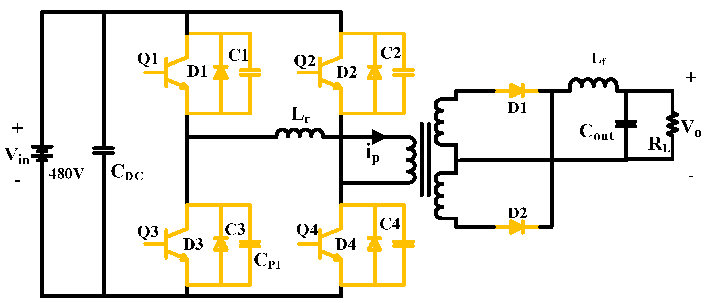
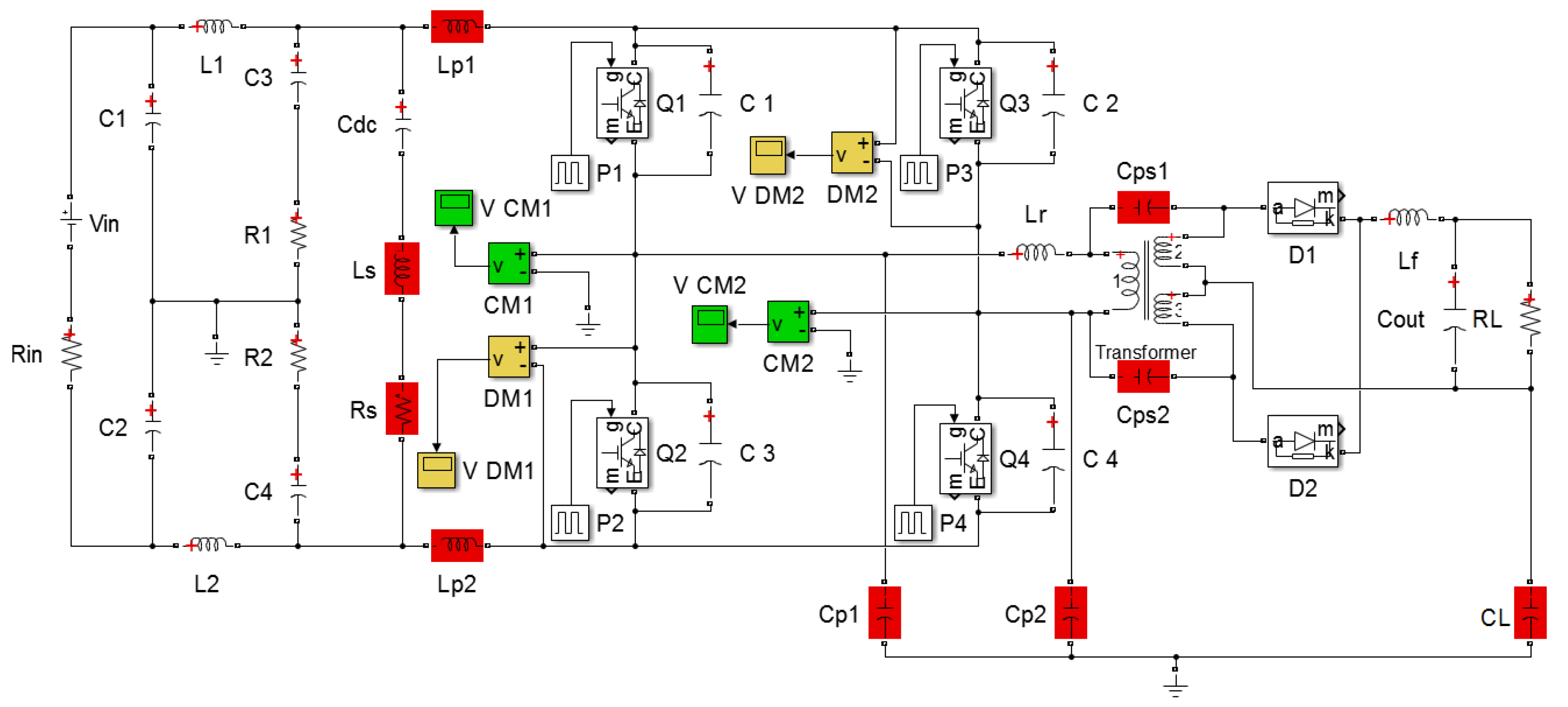
2.1. The Construction of the Onboard DC-DC Converter System

As the indispensable part of EVs, DC-DC converter is used to convert the high dc voltage of the power battery into the low dc voltage to provide power for the low voltage electrical loads. This high-low voltage DC-DC converter system mainly consists of the following parts: high-voltage power battery of EV, DC-DC converter, low-voltage storage battery, and low-voltage load of EV. The Figure 1 below shows the topology of the isolated full-bridge DC-DC converter.
The control mode of phase-shifting PWM is adopted in this topological structure to convert 480 V dc voltage from the power battery into 12 V dc voltage. When considering the high voltage and high frequency characteristics of the DC-DC converter, four MOSFETs, IPP65R150CFDA, with 650 dc voltage are adopted in the full-bridge topology of DC-DC converter. The rising time and falling time of the MOSFET are 7.6 ns and 5.6 ns, respectively.

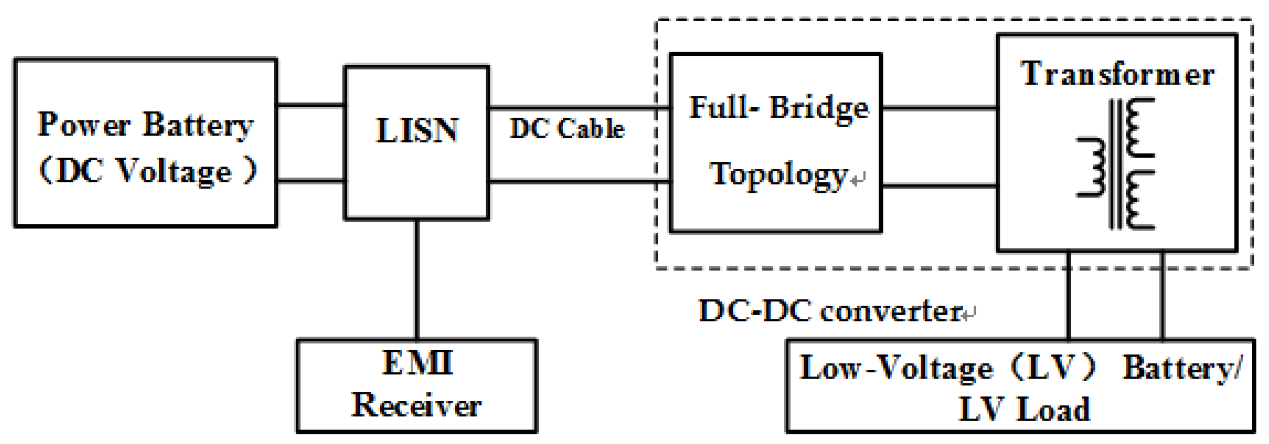
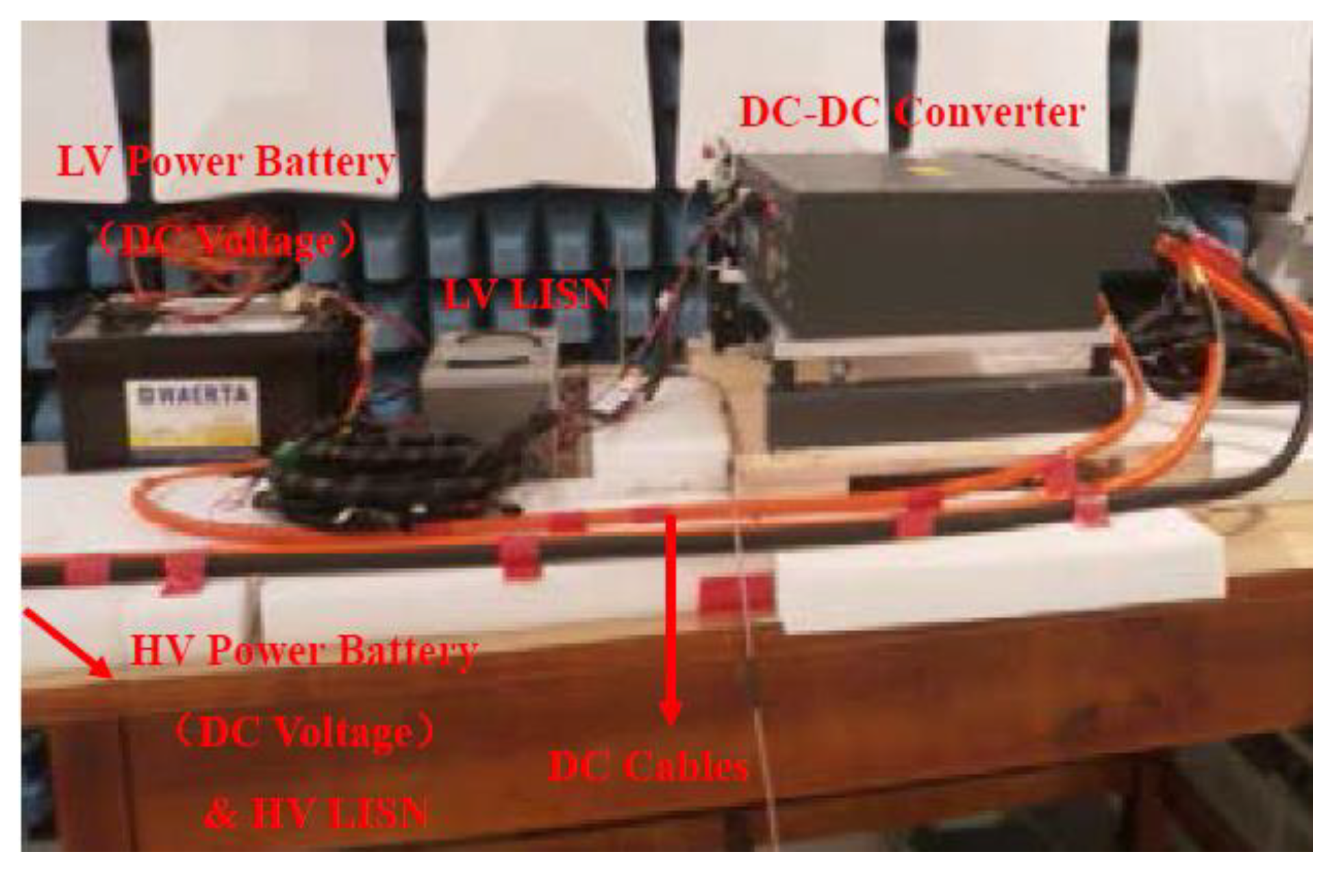
2.2. Setup for Conducted-EMI Emission Test

What shown in Figure 2 is a complete test setup in an EMI laboratory to test the conducted-EMI emissions of the high-low voltage DC-DC converter. It is mainly consisted by a DC voltage source, DC power cables, and standard line impedance stabilization networks (LISNs), full-bridge DC-DC converter, low voltage load, and an EMI receiver. What is shown in Table 1 is the conducted EMI emission limits from 150 kHz to 108 MHz for vehicle components, which is described in standard CISPR 25 (GB/T 18655-2010) complied by measurements. Two LISNs terminated with 50 Ω resistances provide DC power from a DC voltage source to the full-bridge DC-DC converter using two shielded cables (1.5 m). The full-bridge DC-DC converter with 480 V DC input is connected to the low voltage load using two shielded cables (1 m). The DC-DC converter operates at a frequency of 100 kHz. A battery with 12 dc voltage is used as the low voltage. With this configuration, the total conducted-EMI noise voltage signals of DC cables can be obtained through any one of the LISNs that is connected to an EMI receiver.

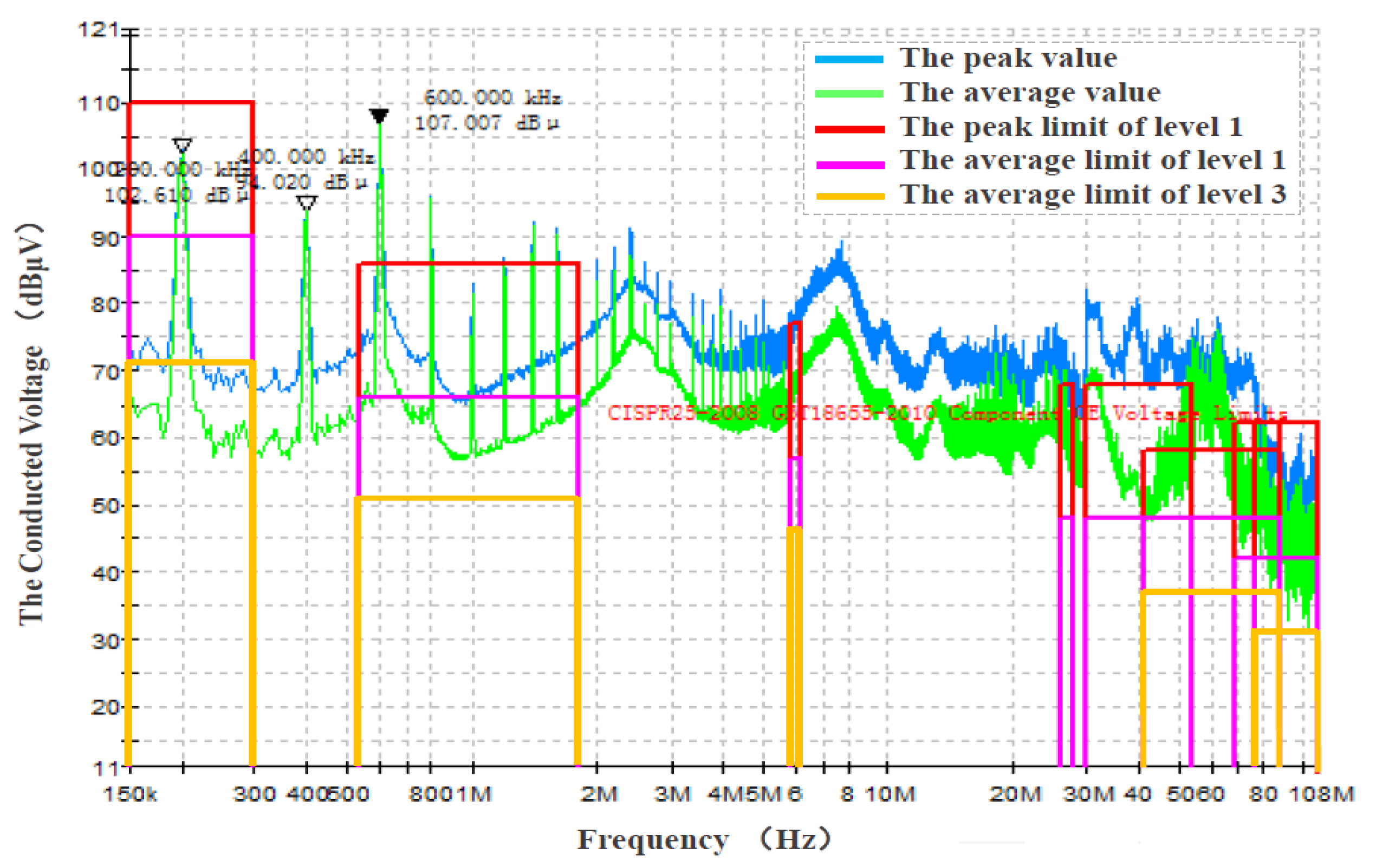
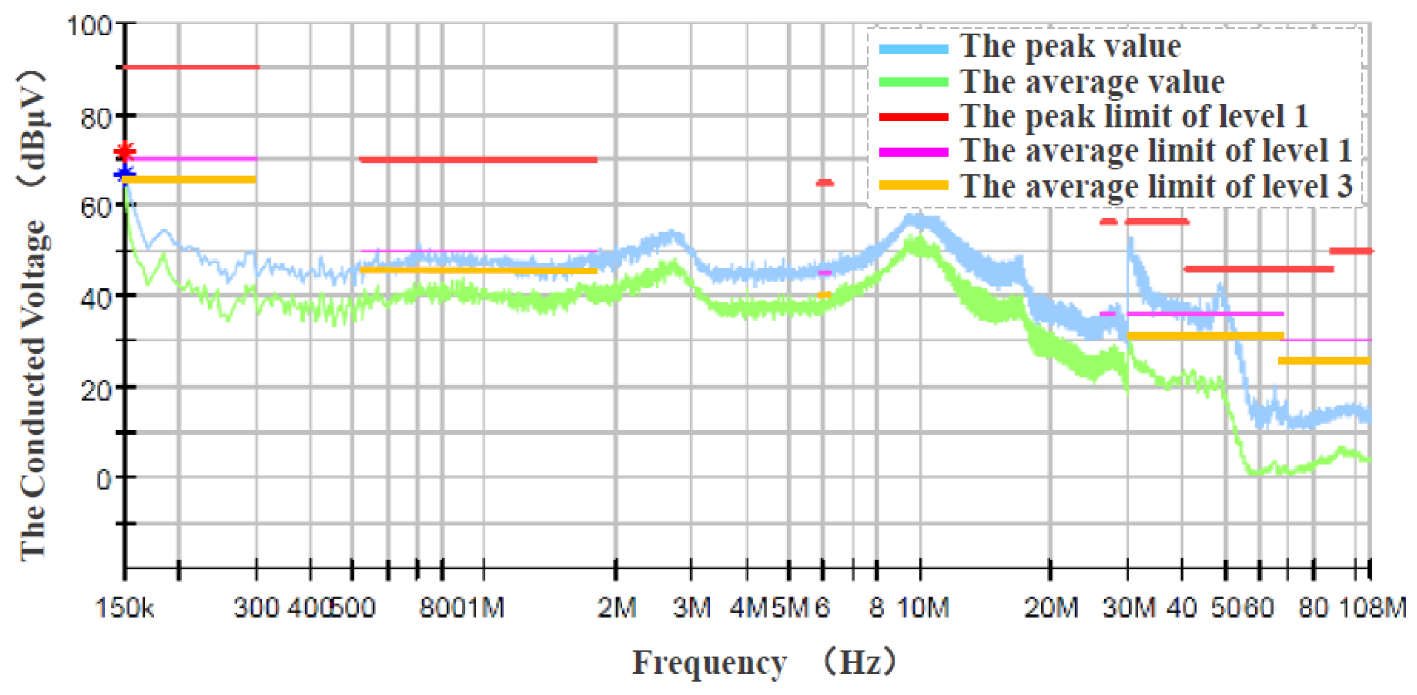
2.3. Experiment Results of the Conducted EMI

The test platform is set up, as shown in Figure 3. Figure 4 shows the experimental results and it can be found that the conducted-EMI noise voltage of the DC-DC converter is dominant in 150 kHz–108 MHz and does not comply with CISPR25(GB/T 18655), as shown in Table 1. In Figure 4, the blue line represents the peak value of the conduction voltage, the green line represents the mean value of the conduction voltage, and the yellow line represents the limit value of standard Level 3. From Figure 4, it can be seen that the frequency bands with excessive conducted voltage are 0.53–1.8 MHz, 5.9–6.2 MHz, 41–88 MHz and 76–108 MHz, and it also includes 200 kHz, 500 kHz–2 MHz, and 30 MHz–108 MHz. Therefore, in order to analyze the source and the paths of the conducted-EMI, the buildup of a high frequency circuit model is necessary, and then the conducted-EMI emissions can be predicted.

2.4. Modeling Analysis of the Onboard DC-DC Converter System
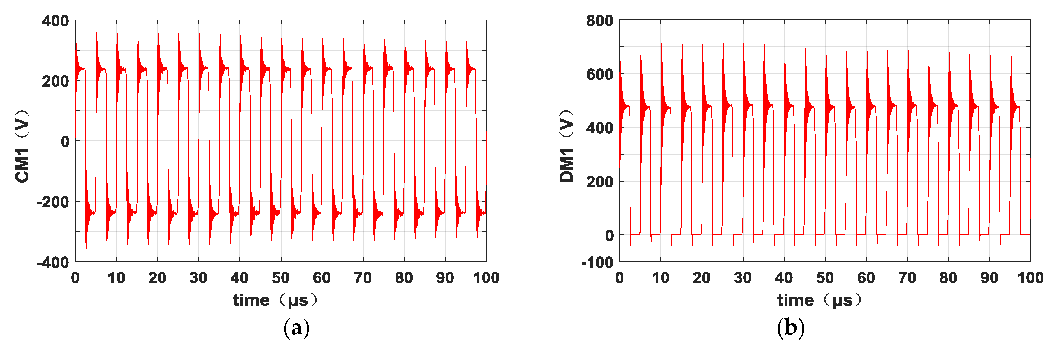
2.4.1. Noise Source

The MOSFETs of the DC-DC converter can switch fast and will cause large dv/dt and di/dt, which can introduce the conducted-EMI emissions. Therefore, the noise source signals of CM interference and DM interference can be obtained from the DC-DC converter legs by measurement. The CM interference voltage source UCM and the DM interference voltage source UDM will be described in detail in the next section.

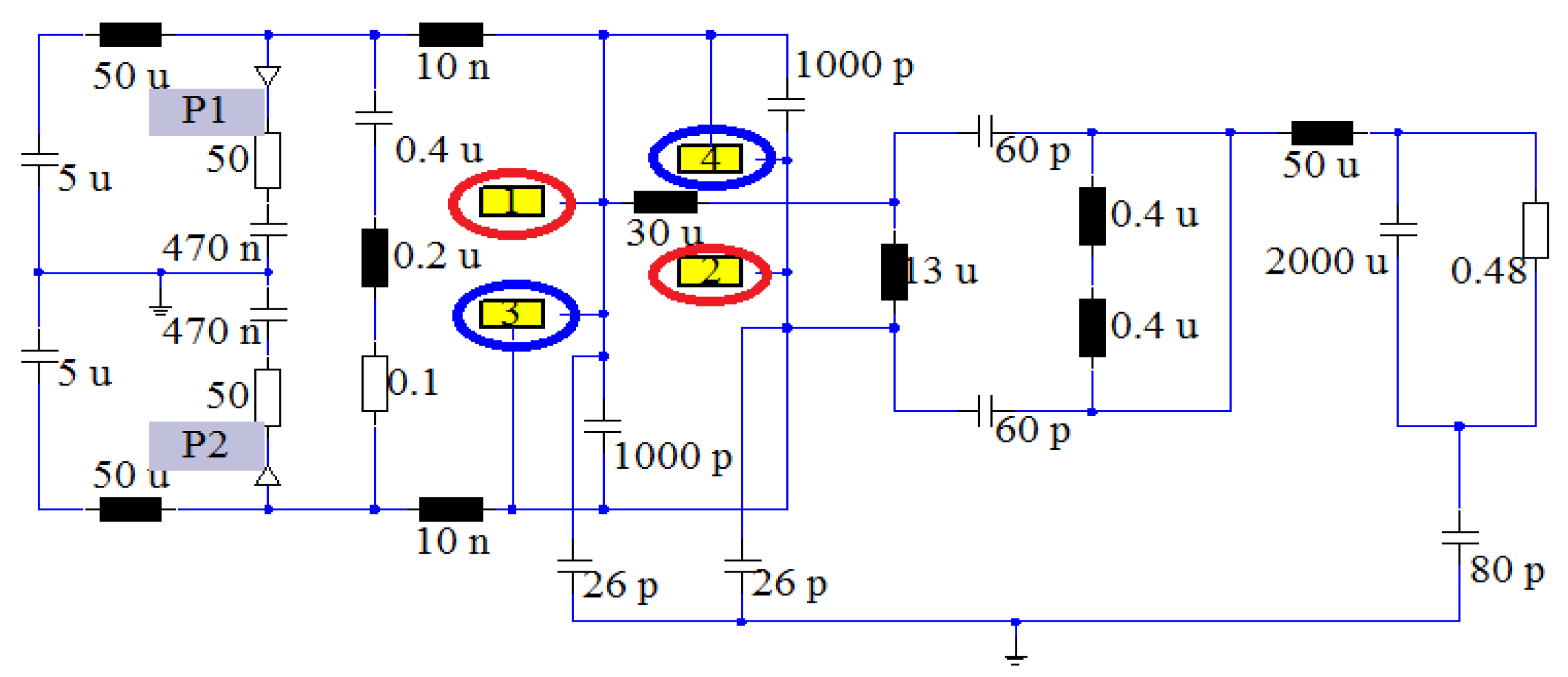
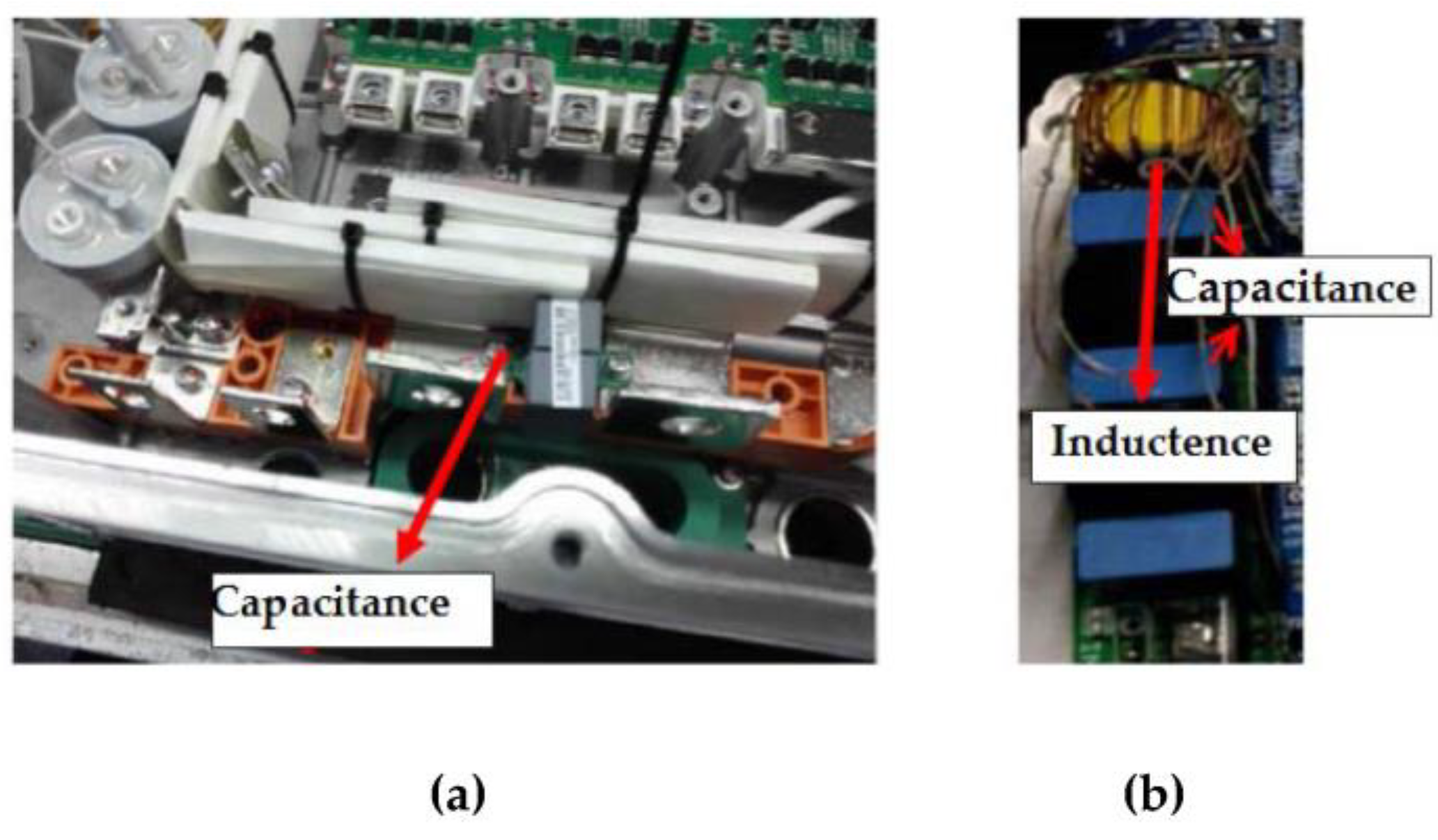
2.4.2. Main Parasitic Parameter

From Figure 5 and Figure 6, there are some parasitic parameters in the DC-DC converter system. It is necessary to extract and determine the parasitic parameters, so that the DC-DC converter for the conducted-EMI can be modeled. Some measurements for Z parameters and S parameters were made with a vector network analyzer and time-domain reflectometry. In order to obtain the high-frequency circuit model of element and system, a modeling method, which is based on a measurement-based model of the electromagnetic emissions, needs to be used. By comparing Z parameters and S parameters of the simulation and measurement, the values of elements, like inductance or capacitance, can be regulated and determined, as shown in Table 2, where, CQ1CQ4 represent the resonant capacitance that is in parallel with MOSFETs Q1–Q4 respectively to achieve ZVS, Lr represents the resonant inductance to achieve ZVS, CDC, Lf, and Cout are all filtering elements, R1, R2, L1, L2, C1C4 represent the components of LISN, RL represent the equivalent resistance of the load, Ls and Rs are the high-frequency parasitic parameters of CDC, Cp1, and Cp2 called the distributed capacitance between the chassis and the midpoints of the leading leg and the lagging leg, Cps1 and Cps2 represent the distributed capacitance of transformer, CL is the distributed capacitance between the load and the chassis. All of these parameters are labeled in Figure 5 and Figure 6.

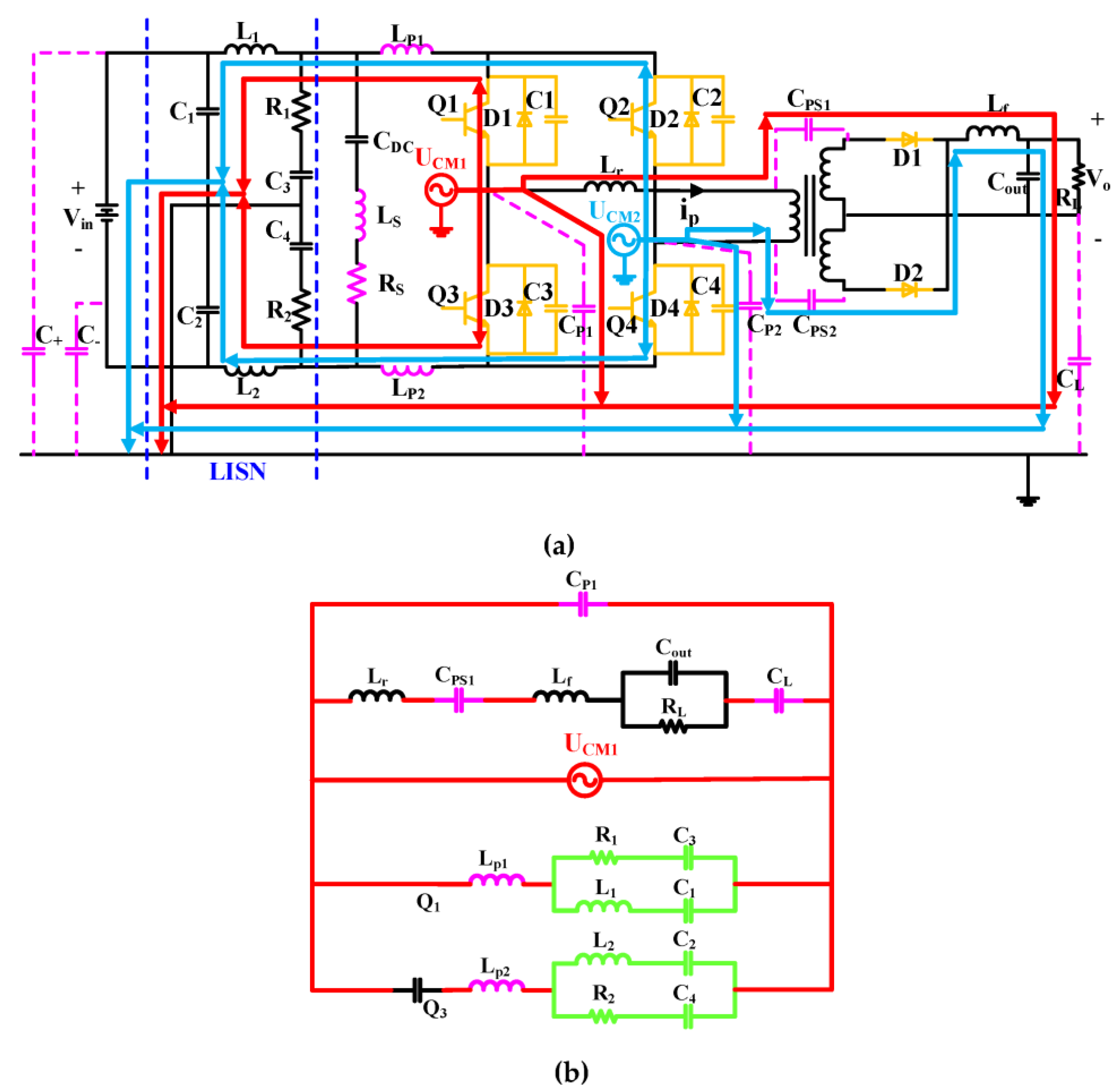
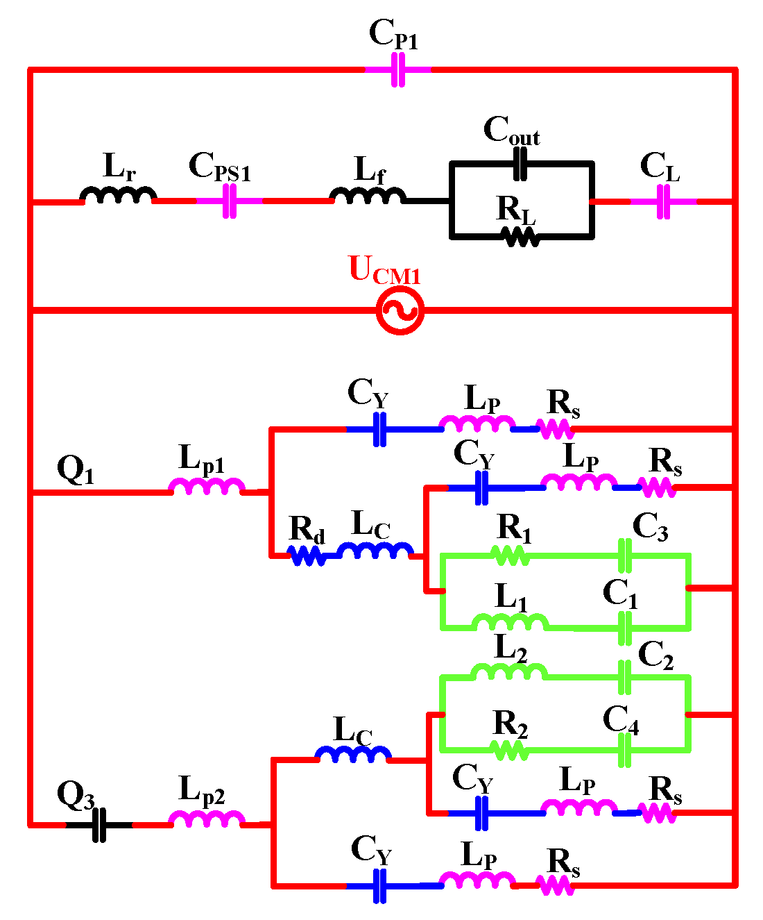
2.4.3. High Frequency Parasitic Parameters of Common Mode EMI

The common mode noise is generated by the displacement current, flowing from the CM interference voltage source UCM to the DC power cables by the parasitic parameters that were connected with the chassis. Cp1, Cps1, Cps2, and CL are the dominated parasitic parameters, which result in CM interference. The main CM paths are shown in Figure 5a. According to Figure 5a, CM paths of UCM1 and UCM2 have similar structures, so only the equivalent circuits of UCM1 are shown in Figure 5b. The four loops for the CM EMI propagation paths through the components can be listed, as follows:
  • Loop 1 for CM1: UCM1Cp1UCM1
  • Loop 1 for CM2: UCM2Cp2UCM2
  • Loop 2 for CM1: UCM1CL ( R L C out ) LfCps1LrUCM1
  • Loop 2 for CM2: UCM2CL ( R L C out ) LfCps2UCM2
  • Loop 3 for CM1: UCM1 ( C 1 L 1 C 3 R 1 ) Lp1UCM1
  • Loop 3 for CM2: UCM2 ( C 4 R 2 C 2 L 2 ) Lp2UCM2
  • Loop 4 for CM1: UCM1 ( C 4 R 2 C 2 L 2 ) CQ3Lp2UCM1
  • Loop 4 for CM2: UCM2 ( C 1 L 1 C 3 R 1 ) Lp1CQ3UCM2
The MOSFET in the closed state is equivalent to short circuit, and it can be represented by conductor; the MOSFET in the open state is replaced by the capacitor in parallel. In addition, no matter which MOSFET produces interference noise, it will always cause the rapid change of the voltage and the current at the midpoint of the bridge leg, so it is most appropriate to choose the middle point of the bridge as the interference source.

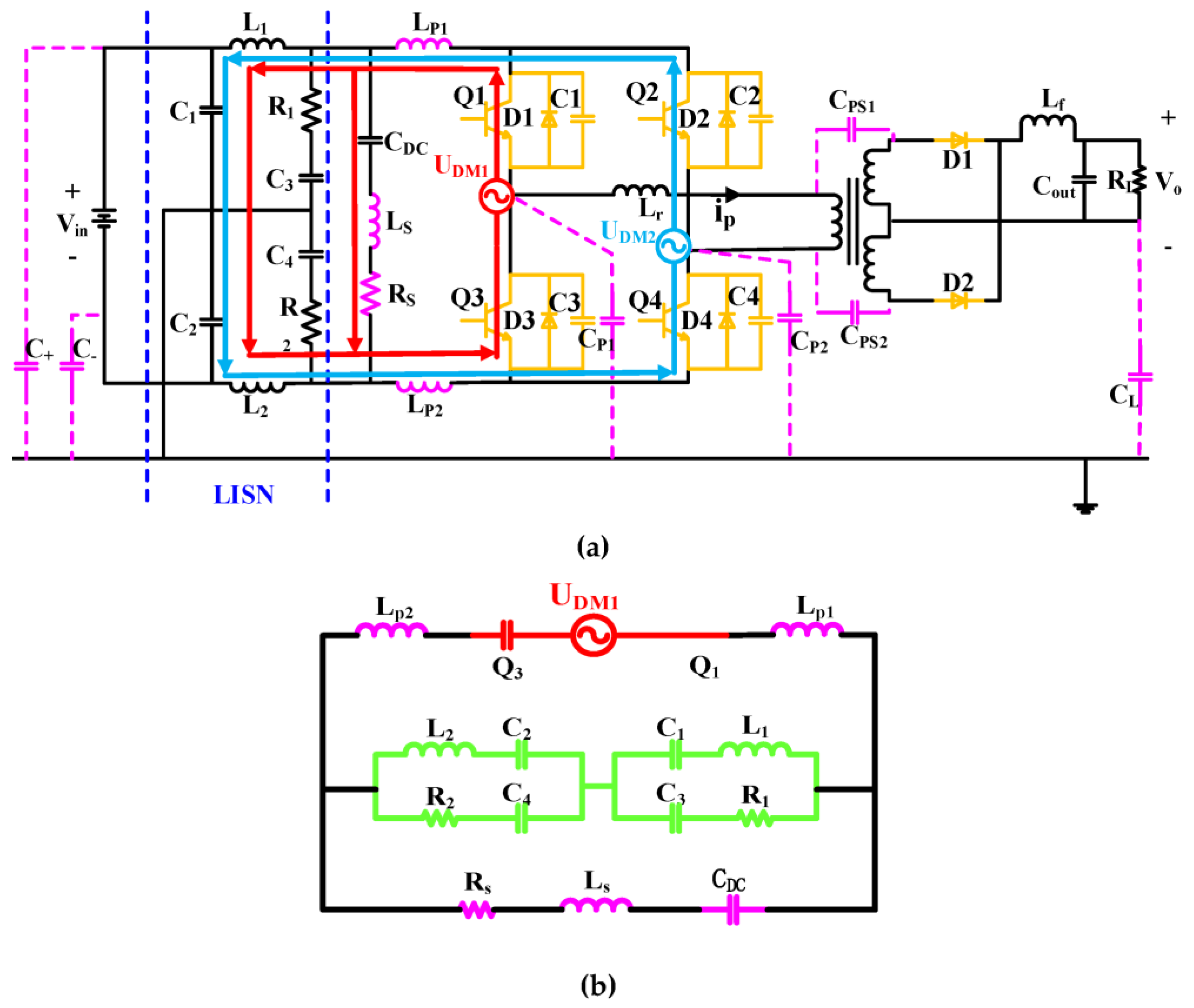
2.4.4. High Frequency Parasitic Parameters of Differential Mode EMI

Similarly, due to the existence of the main DM parasitic parameters, The DM interference can flow through these parasitic inductances and the DM parasitic parameter of the input capacitor to form the DM interference paths. These main parasitic parameters are Lp, Rs, Lp1, and Lp2. Similarly, it can be known that the structures of the DM interference paths of UDM1 and UDM2 are similar. The main DM paths and the equivalent circuits of UDM1 are shown in Figure 6a,b, respectively. The two loops for the DM EMI propagation paths can be listed, as follows:
  • Loop 1 for DM1: UDM1Lp1 ( R 1 C 3 L 1 C 1 ) ( C 4 R 2 C 2 L 2 ) Lp2CQ3UDM1
  • Loop 1 for DM2: UDM2CQ1Lp1 ( R 1 C 3 L 1 C 1 ) ( C 4 R 2 C 2 L 2 ) Lp2UDM2
  • Loop 2 for DM1: UDM1Lp1CDCLsRsLp2CQ3UDM1
  • Loop 2 for DM2: UDM2CQ2Lp1CDCLsRsLp2UDM2

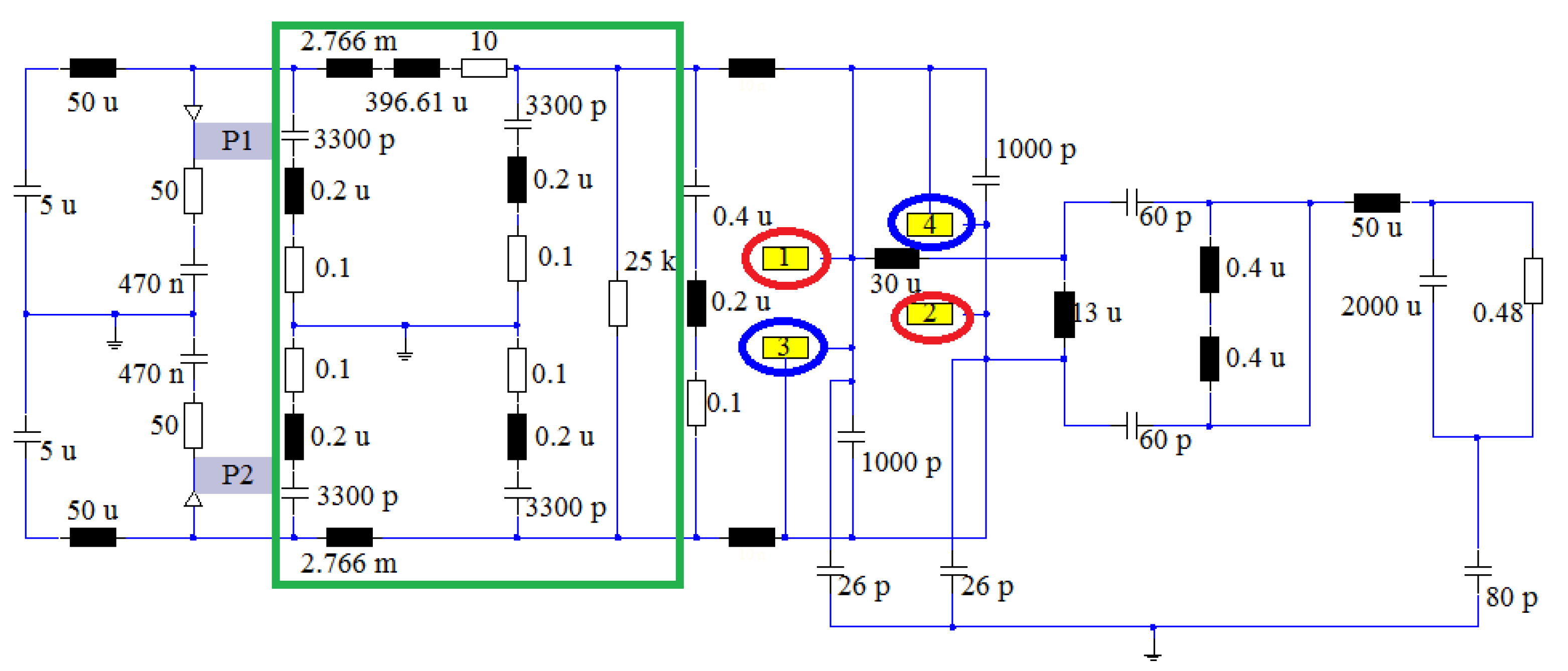
3. Characteristics Analysis and Simulation Prediction for the Conduction Interference

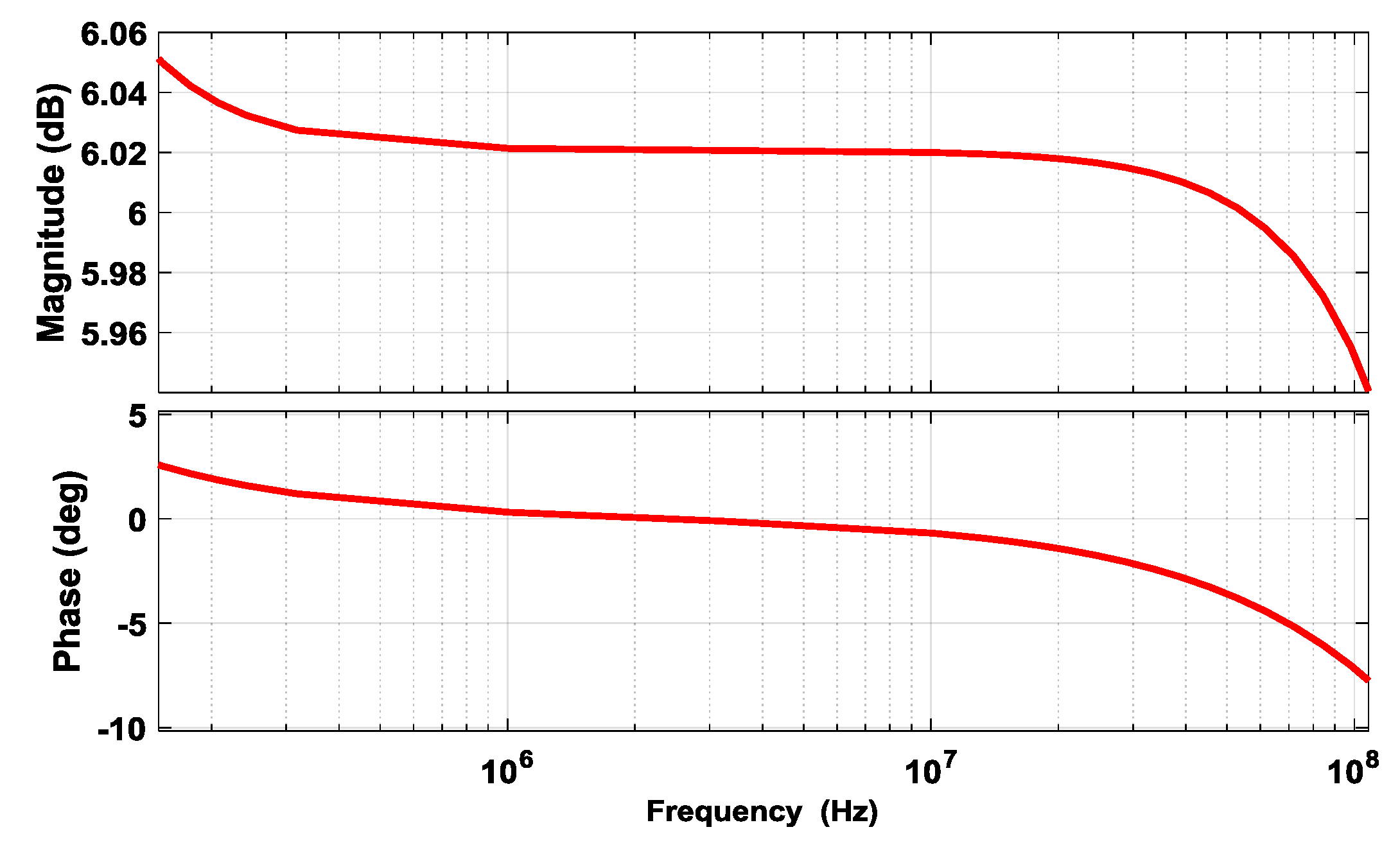
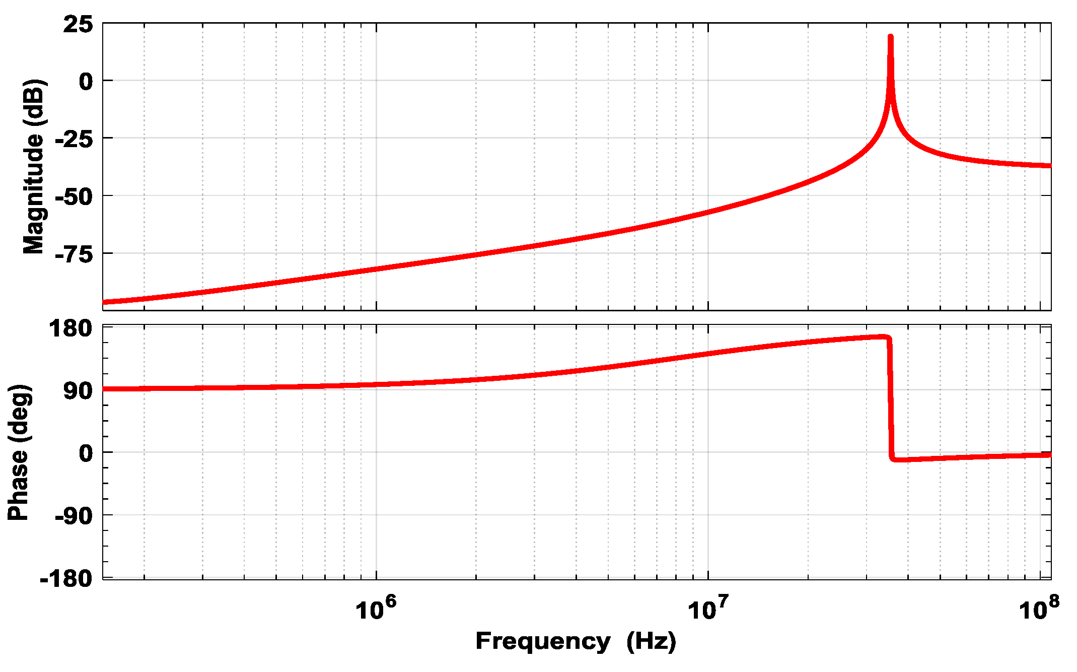
3.1. The Establishment of Transfer Functions

Each noise source can be equivalent to a linear system with single input and single output. Therefore, the two CM transfer functions can be linearly equivalent to the Equation (3), and it is the same to the two DM EMI sources. According to the equivalent circuit of common mode interference paths, the corresponding transfer function of UCM1 is established, as shown in Equation (1), and the Equation (2) can be obtained by substituting the values that are provided in Table 2.
G ( s ) CM 1 = U O _ CM 1 U CM 1 = R 1 ( s L 1 + 1 s C 1 ) ( 1 s C 3 + R 1 ) + ( s L 1 + 1 s C 1 )   ( 1 s C 3 + R 1 ) ( s L 1 + 1 s C 1 ) ( 1 s C 3 + R 1 ) + ( s L 1 + 1 s C 1 ) + s L p 1
G ( s ) CM 1 = 2.35 × 10 11 s 3 + 9.4 × 10 20 47 s 4 + 2.35 × 10 11 s 3 + 10 16 s 2 + 9.4 × 10 20 s + 4 × 10 25
U CM _ O =   G ( s ) CM 1 × U CM 1 +   G ( s ) CM 2 × U CM 2
The Bode diagram, as shown in Figure 7, can be obtained by the transfer function of Equation (2). From Figure 7, it can be seen that large CM conducted interference exists within 150 kHz–30 MHz. The interference is especially obvious in the lower frequency band before 300 kHz, and it begins to drop at 30 MHz. Hence, it can be seen that the CM conducted interference mainly exists in the frequency bands before 30 MHz.
Similarly, the transfer function of the DM1 interference paths can be obtained, as shown in Equation (5), and Equation (6) is its numerical expression. The DM bode diagram that is obtained by the transfer function (7) is shown in Figure 8. From Figure 8, it shows that the DM conducted interference is relatively smaller in low frequency band, and there exists a peak value at frequency from 30 MHz to 40 MHz due to the circuit resonance. Therefore, it can be known from Figure 7 and Figure 8 that CM interference is the dominated interference in the frequency band from 150 kHz to 108 MHz.
Z LISN ( DM ) = ( 1 s C 3 + R 1 ) ( s L 1 + 1 s C 1 ) ( 1 s C 3 + R 1 ) + ( s L 1 + 1 s C 1 ) + ( 1 s C 4 + R 2 ) ( s L 2 + 1 s C 2 ) ( 1 s C 4 + R 2 ) + ( s L 2 + 1 s C 2 )
G ( s ) DM 1 = U O _ DM 1 U DM 1 = Z LISN ( DM ) / / ( 1 s C D C + s L s + R s ) s L p 1 + Z LISN ( DM ) / / ( 1 s C D C + s L s + R s ) + s L p 2 + 1 s C Q 3
G ( s ) DM 1 = 1.56 s 6 + 7.81 × 10 7 s 5 + 3.64 × 10 12 s 4 + 3.12 × 10 17 s 3 + 1.45 × 10 22 s 2 252 s 6 + 8.88 × 10 7 s 5 + 1.25 × 10 19 s 4 + 5.32 × 10 23 s 3 + 2.50 × 10 30 s 2 + 1.06 × 10 35 s + 1.13 × 10 36
U DM _ O =   G ( s ) DM 1 × U DM 1 +   G ( s ) DM 2 × U DM 2

3.2. Extraction of the Noise Sources

According to Figure 9, a circuit model with high-frequency parameters of the DC-DC converter system is built in Matlab/Simulink, so that the noise source signals of CM interference and DM interference can be obtained. All of the main parasitic parameters are shown in red background. The two CM sources are the voltage between the midpoint of the bridges of the DC-DC converter and the chassis, as shown in green background. The two DM sources are the voltage between the midpoint of the bridges of the DC-DC converter and the negative or the positive terminal, as shown in yellow background. The CM and the DM noise source signals of the advanced bridge are shown in Figure 10a,b, respectively.

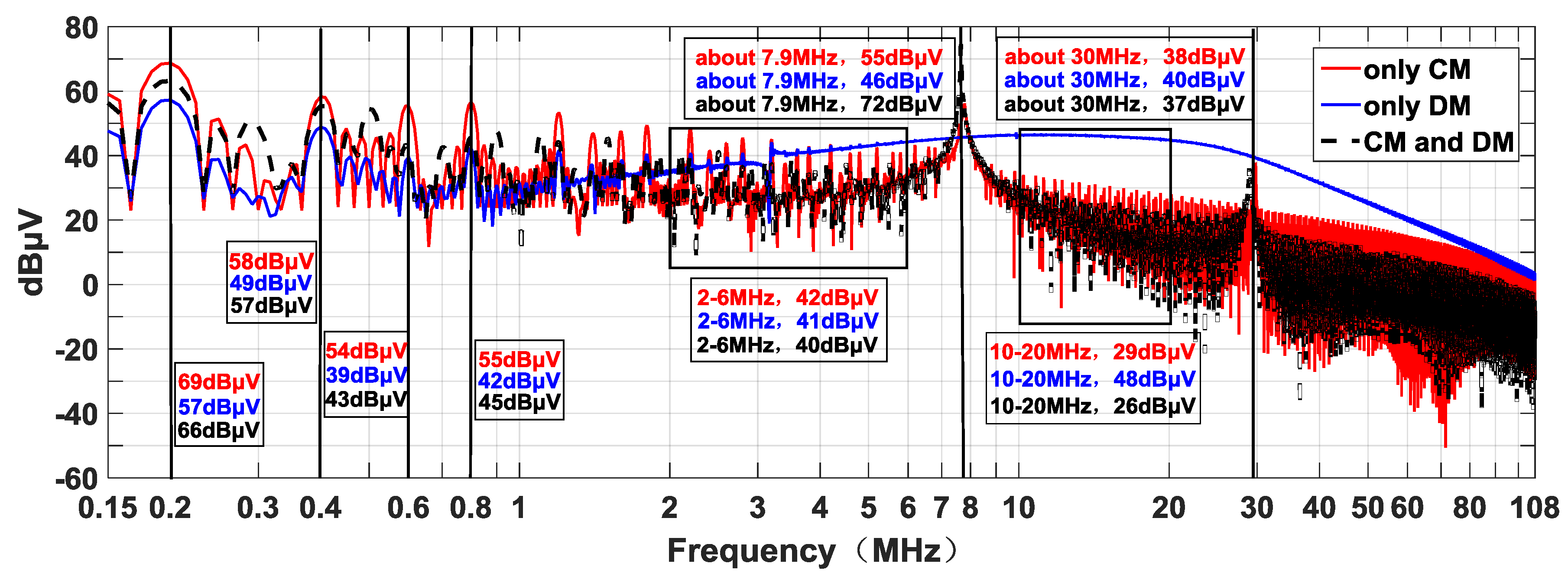
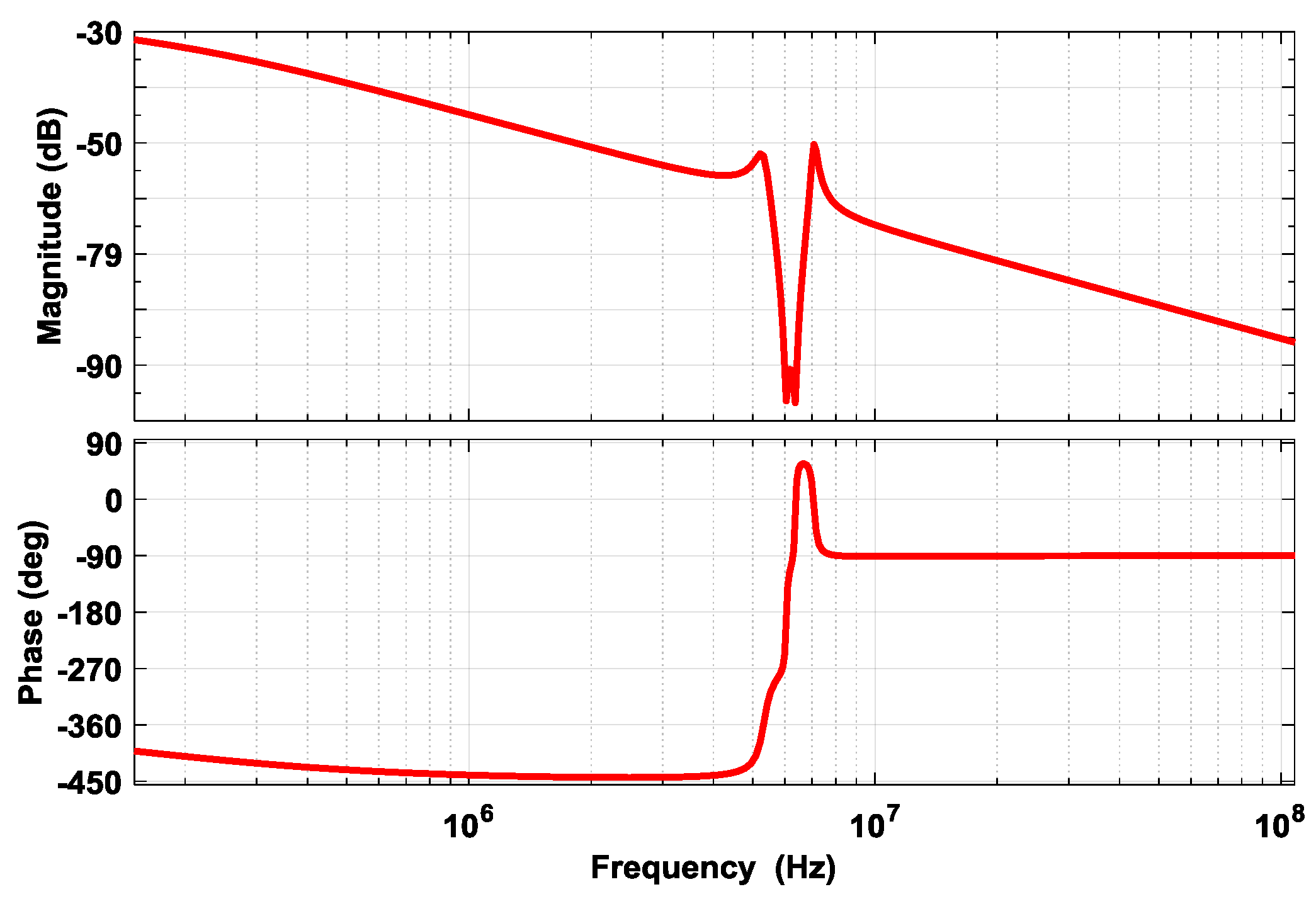
3.3. Simulation for the Conducted Interference

The conducted interference both in the time domain and in the wide-range frequency domain can be obtained by Computer Simulation Technology (CST). The conducted interference voltage that is shown in Figure 11 can be obtained by establishing the high-frequency circuit model of the DC-DC converter in CST. The acquisition of the signals of the DM and CM interference sources UCM1 (UCM2) and UDM1 (UDM2) can achieved in Matlab/Simulink, as shown in Figure 10. As the important indicator for conducted-EMI, the conducted interference voltage can be obtained by modeling the LISNs consisting of R1, R2, L1, L2, C1–C4 and adding probe “P1” and “P2”, port 1 and port 2 in red circles are CM ports, port 3 and port 4 in blue circles are DM ports, which are all shown in Figure 11.
The positive conducted voltage of the single mode and CM+DM, which can be measured by the LISN, is compared in Figure 12. The conducted voltage of the CM+DM mode is represented by the black curve, the CM conducted voltage is represented by the red curve and the DM conducted voltage is represented by the blue curve. It can be seen that some resonances appear at the same frequency 200 kHz, 400 kHz, 600 kHz, 800 kHz etc. which have the same frequency interval. In addition, there are two resonance points at 7.8 MHz and 30 MHz in the CM mode and the hybrid mode. In terms of the conducted voltage in Figure 12, the CM+DM waveform, in fact, can be better represented by the CM waveform of the conducted voltage, and the CM conducted EMI is the dominated interference in a frequency range of 150 kHz–108 MHz.
There is good consistency between the simulation result of the conducted voltage and the change of the Bode diagram by transfer function. Therefore, from Figure 7 and Figure 12, it can be concluded that the CM interference is mainly responsible for the conducted-EMI from the DC high voltage power cables of the DC-DC converter.

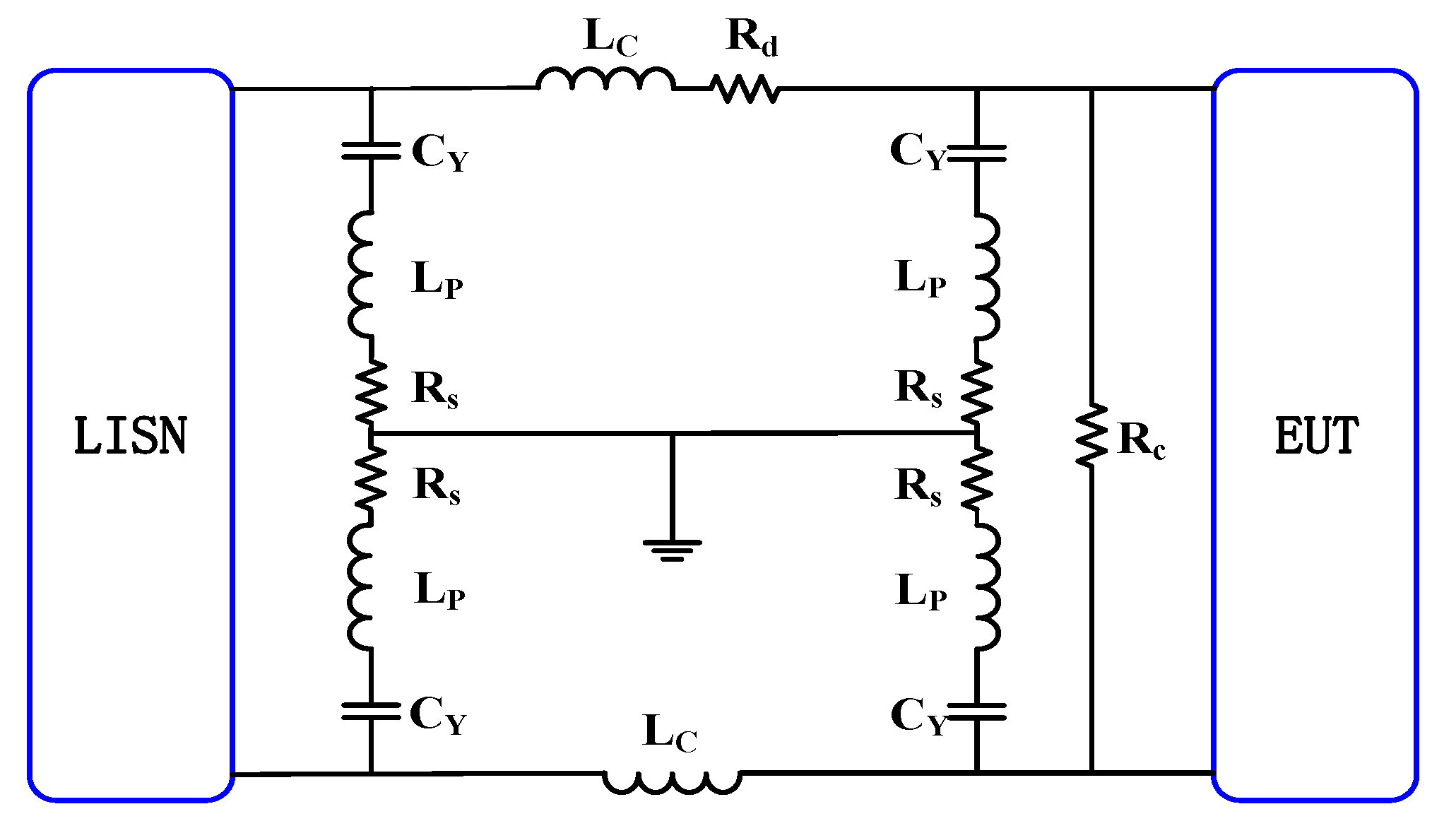
4. Design of High Frequency EMI Filter

From the discussion above, the conducted EMI of the high-low voltage DC-DC converter mainly comes from the CM interference. Therefore, the design for the CM filter is given priority to take into account in order to mitigate the conducted-EMI from the high-low voltage DC-DC converter in EVs.

4.1. Parameters Calculation of CM EMI Filter

The insertion loss method is adopted to calculate the values of the main passive components in the EMI filter. Firstly, the attenuations of the CM interference should be determined. The required attenuation amounts ACM of the CM interference can be obtained through Equation (8):
A CM [ d B μ V ] = A nCM A L + m
The AnCM is the amplitude of the nth harmonic (in the case of the fundamental frequency of 100 kHz); AL is the limit of CISPR25/GB/T18655 level 3 in the frequency band from 150 kHz to 108 MHz; AL is 50 dBμV in the frequency range of 0.53–1.8 MHz; and, m is 6 dBμV, the safety margin of filter suppression.
The influence of CM interference is dominant in the high frequency band, therefore, according to the test result and its limit line of Level 3 in Figure 4 and following the principle that, it can be known that the superscalar of CM interference reaches the maximum value of 43 dBμV at 1.4 MHz, and the AnCM is 93 dBμV. Thus, the target attenuation frequency of the CM interference is 1.4 MHz. When considering the safety margin of 6 dBμV, the target attenuation of the CM is 49 dBμV. Areq_att [dBμV] is the target attenuation of CM.
Then, the corner frequency (cutoff frequency) f0 of the CM filter needs to be obtained by calculating. In order to restrain the interference effectively, the corner frequency of the filter must be low enough, so that they can meet the suppression demand in the whole frequency band required. In generally, the corner frequency is calculated by using the frequency (i.e., 1.4 MHz) of the first highest interference amplitude point of CM interference (see in Equation (9)).
f 0 = f h _ att 10 A req _ att f i l t e r _ a t t
where fh_att is the frequency for attenuation; Areq_att is the attenuation; filter_att is the slope of the attenuation slash, 40 dB/dec. The attenuation frequency of CM that was obtained by Equation (9) is 37.25 kHz.
The CM inductance LC and the CM capacitance CY of the CM filter can be calculated by the Equation (10):
L C = ( 1 2 π f 0 ) 2 × 1 2 C Y
It is usually assumed that CY takes the normal value, 3300 pF, so the value of LC can be calculated as 2.766 mH.

4.2. Topology Selection of CM Filter

In order to determine the best CM filter topology, the volume and weight of the filter are both considered, four different topologies are designed and inserted into the high-frequency model in CST, respectively. And these four kinds of topologies include the topology of capacitance + inductance (CL), the topology of inductance + capacitance (LC), the topology of capacitance + inductance + capacitance (CLC) and the topology of inductance + capacitance + inductance (LCL). The comparison in attenuation between the four kinds of filters is shown Figure 13, the attenuation values at some important frequency points are listed, and the corresponding curves of CLC, LCL, CL, and LC are presented in pink, sky blue, blue, and brown, respectively. From Figure 13, it can be seen that the topologies of LCL and CLC have the better suppression effect than that of CL and LC in the low-frequency band (less than 500 kHz), and the CLC topology has an obviously better suppression effect than other topologies at the frequency from 150 kHz to 180 MHz. Besides, CLC has a smaller volume than LCL. By considering both the suppression effect in the whole frequency band and the size of the filter, the optimal topology of the CM filter for the high-low voltage DC-DC converter is CLC, as shown in Figure 14. Rd (25 kΩ) and Rc (10 Ω)are the equivalent impedance of the filter, LP (0.2 μH) and Rs (0.1 Ω) are the high frequency parasitic parameters of CY, respectively.
In order to verify the suppression effect of the CM filter with CLC topology in Figure 14, a simulation model with the CLC topology for the high-low voltage DC-DC converter is established in CST, as shown in Figure 15. The conducted voltage of simulation results with and without the CM filter with CLC topology are shown in Figure 16.
From Figure 16, it can be known that the conducted voltage of simulation has a sharp reduction in the whole frequency band of 150 kHz–108 MHz. Most important of all, the conducted voltage is decreased by 55 dBμV at the target frequency 1.4 MHz and it meets the designed attenuation 49 dBμV very well. The detail values of the conducted voltage with and without the CM filter are listed in Table 3.

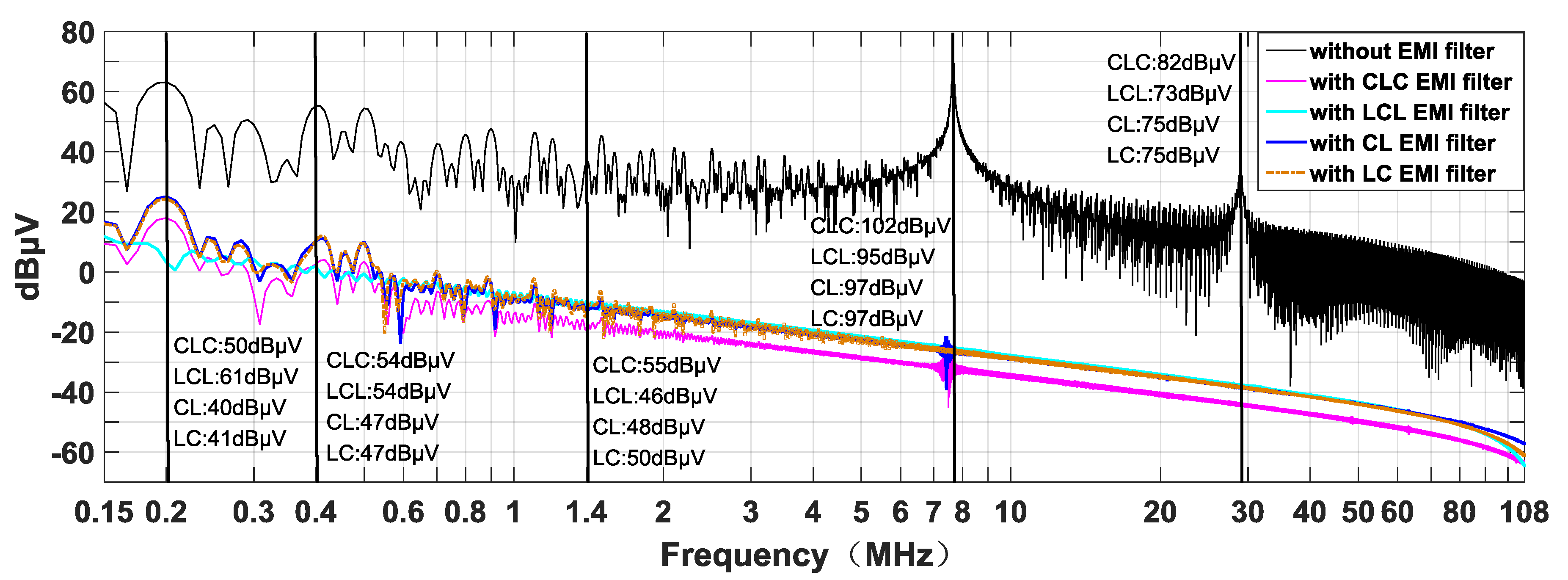
4.3. Mitigation Effect and Stability Analysis of the High Frequency EMI Filter

The high frequency parameters of the filters have an important effect on its stability. The equivalent circuit with the CLC filter is shown in Figure 17. The corresponding transfer function is expressed by the numerical equation, as shown in Equation (12).
G CM 1   filter ( s ) = 6.9 e 13 s 12 + 1.25 e 38 s 11 + 1.25 e 44 s 10 + 3.8 e 53 s 9 + 1.9 e 59 s 8 + 2.88 e 68 s 7 + 7.58 e 68 s 6 4.01 e 9 s 13 + 7.25 e 33 s 12 + 6.32 e 28 s 11 + 2.24 e 49 s 10 + 2.78 e 40 s 9 + 1.6 e 64 s 8 + 1.63 e 70 s 7 +   1.15 e 78 s 5 + 3.99 e 70 s 4 + 2.76 e 76 s 3 + 1.39 e 81 s 2 + 1.06 e 86 s + 4.91 e 90 + 7.98 e 74 s 6 + 3.83 e 78 s 5 + 4.38 e 72 s 4 + 1.68 e 78 s 3 + 1.44 e 83 s 2 + 3.77 e 87 s + 1.64 e 91
U CM _ O =   G ( s ) CM 1   filter × U CM 1 +   G ( s ) CM 2   filter × U CM 2
According to Equation (12), the corresponding Bode diagram can be obtained, as shown in Figure 18. It can be seen that the magnitude is decreased by the expectation attenuation. There is no new resonance appearance at the whole frequency band 150 kHz–108 MHz. From Figure 18, the DC-DC converter with the CM filter has better stable characteristics and can achieve a good mitigation effect for the conducted EMI.
From Figure 18, it can be seen that the conducted voltage can be decreased by a continuous attenuation (from −40 dBμV to −95 dBμV) in 150 kHz–108 MHz. When comparing with the Bode diagram without the CM filter in Figure 7, it can be seen that the amplitude has sharply reduced.

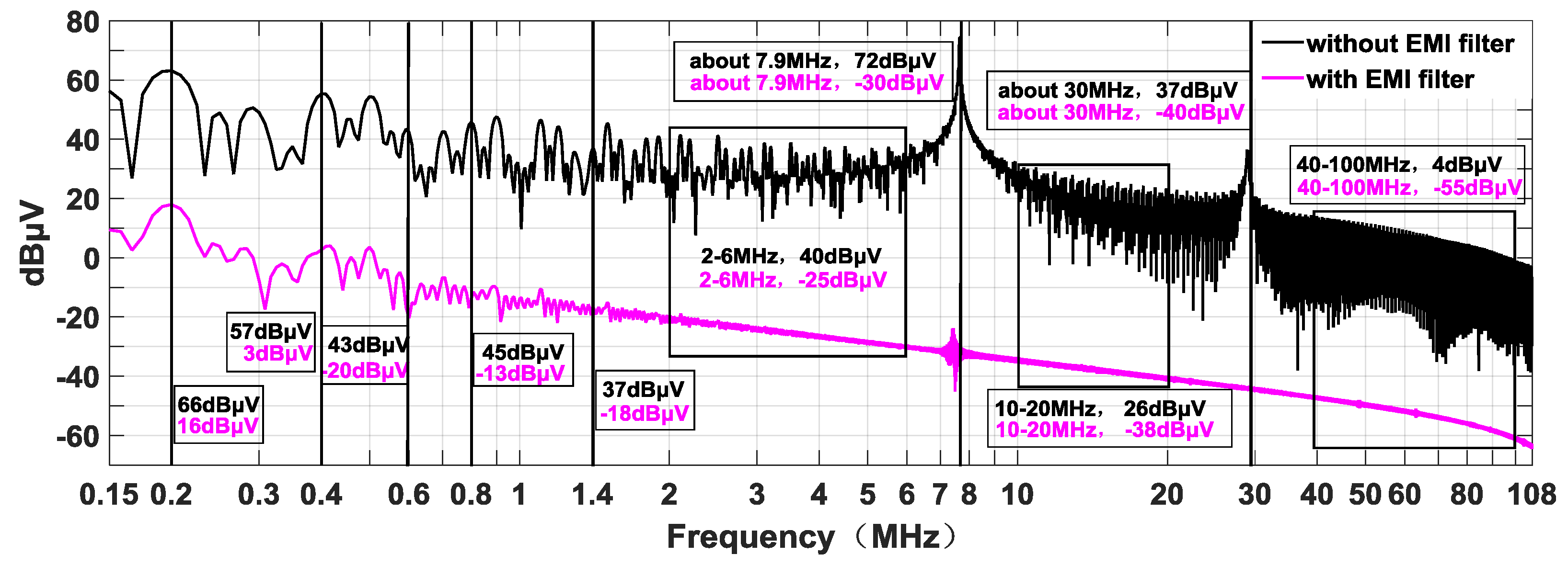
5. Experimental Verification

Comparison and Analysis for the EMI Experimental Result and EMI Simulation Result

A conducted voltage experiments is built by CISPR 25(GB/T18655), as shown in Figure 3, to validate the suppressive effect of the CM filter with CLC topology. The CM filter with CLC topology is added at DC input terminals inside the high-low voltage DC-DC converter, as shown in Figure 19. After inserting the CLC filter, the measurement result of the conducted voltage on the primary DC power cable can be seen in Figure 20.
From Figure 20, the conducted voltage is lower than the limit of CISPR 25(GB/T18655) in the whole frequency band and it meets the standard requirements. The attenuation comparison of the experiment results and simulation results is listed in Table 4. It can be seen that the attenuation results of simulation and experiment are basically identical (roughly the same amount of interference suppression). In those important resonant points and frequency band, the attenuation errors between the experiment results and simulation results are very small, which validate the availability of the proposed high-frequency model and the designed EMI filter. Besides, it notes that the attenuation at 1.4 MHz is 53 dBμV, which matches the simulation result 55 dBμV and meets the target attenuation 49 dBμV very well. In addition, the harmonics results of simulation that start from 200 kHz with the interval of 200 kHz match the harmonics results of the experiment very well. In addition, the harmonic amplitude of the experiment is significantly greater than that of the simulation due to real operating condition.

6. Conclusions

A conducted EMI prediction and mitigation strategy that is based on transfer function for the high-low voltage DC-DC converter in EVs are proposed. The equivalent circuits of the CM and DM interference for the DC-DC converter are built based on the measurement results of high-frequency parasitic parameters. The characteristics of the conducted EMI from the DC power cables are obtained. The dominated conducted EMI is predicted by establishing the corresponding transfer functions of the DM interference and CM interference. By analyzing the transfer functions and the simulation results, the CM interference is known as the dominated interference that is responsible for the conducted EMI. By the simulation and the experiment, a strategy of giving priority to the dominated interference mode is proposed for designing the optimal CM interference filter with CLC topology. From the experiment results, the conducted voltage of the DC power cables is decreased, respectively, by 58 dBμV, 55 dBμV, 65 dBμV, 53 dBμV, and 54 dBμV at frequency 200 kHz, 400 kHz, 600 kHz, 1.4 MHz, and 50 MHz. The conduced voltage in frequency range from 150 kHz to 108 MHz can be mitigated to below the limit level-3 of CISPR25 standard (GB/T 18655-2010) by adding the CM interference filters. The DC-DC converter with the CM filter has better stable characteristics and can achieve a good mitigation conducted EMI effect. In the future, the equivalent circuit model for the high-low voltage DC-DC converter should be improved in the frequency 30 MHz–108 MHz to predict the radiated EMI from the DC power cables of the DC-DC converter.

Author Contributions

Li Zhai and Tao Zhang designed the methodology and wrote the manuscript. Yu Cao and Sipeng Yang conceived and design the experiments. Steven Kavuma and Huiyuan Feng implemented the experiments. All authors contributed improving the quality of the manuscript.

Acknowledgments

This paper was supported by the National Natural Science Foundation of China for financially supporting this project (51475045).

Conflicts of Interest

The authors declare no conflict of interest.

References

  1. Ferrero, E.; Alessandrini, S.; Balanzino, A. Impact of the electric vehicles on the air pollution from a highway. Appl. Energy 2016, 169, 450–459. [Google Scholar] [CrossRef]
  2. Zhai, L.; Zhang, X.; Bondarenko, N.; Loken, D.; Van Doren, T.P.; Beetner, D.G. Mitigation Emission Strategy Based on Resonances from a Power Inverter System in Electric Vehicles. Energies 2016, 9, 419. [Google Scholar] [CrossRef]
  3. Zhai, L.; Lin, L.; Zhang, X.; Song, C. The Effect of Distributed Parameters on Conducted EMI from DC-Fed Motor Drive Systems in Electric Vehicles. Energies 2016, 10, 1. [Google Scholar] [CrossRef]
  4. Xue, J.; Wang, F. Modeling and design of common-mode inductor for conductive EMI noise suppression in DC-fed motor drive system. In Proceedings of the Energy Conversion Congress and Exposition, Raleigh, NC, USA, 15–20 September 2012; pp. 645–651. [Google Scholar]
  5. Kahoul, R.; Marchal, P.; Azzouz, Y.; Mazari, B. HF model of DC motor impedance EMC problems in automotive applications. In Proceedings of the IEEE International Symposium on Electromagnetic Compatibility, Detroit, MI, USA, 18–22 August 2008; pp. 1–5. [Google Scholar]
  6. Song, B.; Tao, Y. The suppression of conducted EMI for the motor controller in a battery electric vehicle. Automot. Eng. 2013, 35, 996–999. [Google Scholar]
  7. Kahoul, R.; Azzouz, Y.; Ravelo, B.; Mazari, B. New Behavioral Modeling of EMI for DC Motors Applied to EMC Characterization. IEEE Trans. Ind. Electron. 2013, 60, 5482–5496. [Google Scholar] [CrossRef]
  8. He, H.; Qu, B.; Chen, C.; Bai, B. Research on the EMI suppression methods of the integrative motor system. In Proceedings of the International Conference on Electrical Machines and Systems, Beijing, China, 20–23 August 2011; pp. 1–4. [Google Scholar]
  9. Diouf, F.; Leferink, F.; Duval, F.; Bensetti, M. Wideband Impedance Measurements and Modeling of DC Motors for EMI Predictions. IEEE Trans. Electromagn. Compat. 2014, 57, 180–187. [Google Scholar] [CrossRef]
  10. Kubik, Z.; Skala, J. Industrial DC/DC converters in terms of EMC. In Proceedings of the Compatibility and Power Electronics, Tallinn, Estonia, 1–3 June 2011; pp. 295–298. [Google Scholar]
  11. Ali, M.; Labouré, E.; Costa, F.; Revol, B. Design of a Hybrid Integrated EMC Filter for a DC–DC Power Converter. IEEE Trans. Power Electron. 2012, 27, 4380–4390. [Google Scholar] [CrossRef]
  12. Ali, M.; Laboure, E.; Costa, F.; Revol, B.; Gautier, C. Hybrid Integrated EMC filter for CM and DM EMC Suppression in a DC-DC Power converter. In Proceedings of the International Conference on Integrated Power Electronics Systems, Nuremberg, Germany, 6–8 March 2012; pp. 1–6. [Google Scholar]
  13. Grobler, I.; Gitau, M.N. Conducted EMC modeling for accreditation in DC-DC converters. In Proceedings of the IECON 2015—41st Annual Conference of the IEEE Industrial Electronics Society, Yokohama, Japan, 9–12 November 2015; pp. 002329–002335. [Google Scholar]
  14. Huynh, H.A.; Joo, S.; Kim, S. An experimental study of EMI reduction of DC-DC converter with frequency hopping technique. In Proceedings of the Electrical Design of Advanced Packaging and Systems, Honolulu, HI, USA, 14–16 Decemebr 2016; pp. 107–109. [Google Scholar]
  15. Ales, A.; Schanen, J.L.; Moussaoui, D.; Roudet, J. Impedances Identification of DC/DC Converters for Network EMC Analysis. IEEE Trans. Power Electron. 2014, 29, 6445–6457. [Google Scholar] [CrossRef]
  16. Koo, K.; Kim, J.; Kim, M.; Kim, J. Impact of PCB design on switching noise and EMI of synchronous DC-DC buck converter. In Proceedings of the IEEE International Symposium on Electromagnetic Compatibility, Fort Lauderdale, FL, USA, 25–30 July 2010; pp. 67–71. [Google Scholar]
  17. Luo, F.L.; Ye, H. Investigation of EMI, EMS and EMC in power DC/DC converters. In Proceedings of the International Conference on Power Electronics and Drive Systems, Singapore, 17–20 November 2003; Volume 1, pp. 572–577. [Google Scholar]
  18. Mukharjee, I.; Gadoura, I.A. Simple, low EMI-noise input-filter design for DC/DC power regulators. In Proceedings of the Industrial Electronics and Applications, Singapore, 18–20 July 2012; pp. 948–953. [Google Scholar]
  19. Karvonen, A.; Astrom, J. Simulating the EMI characteristics of step-down DC/DC converters. In Proceedings of the Vehicle Power and Propulsion Conference, Chicago, IL, USA, 6–9 September 2011; pp. 1–6. [Google Scholar]
  20. Wang, Q.; An, Z.; Zheng, Y.; Yang, Y. Parameter extraction of conducted electromagnetic interference prediction model and optimisation design for a DC-DC converter system. IET Power Electron. 2013, 6, 1449–1461. [Google Scholar] [CrossRef]
  21. Gao, X.; Su, D.; Li, Y. Study on electromagnetic interference of DC/DC converter used in the EV. In Proceedings of the 2015 Asia-Pacific Symposium on Electromagnetic Compatibility (APEMC), Taipei, Taiwan, 26–29 May 2015; pp. 258–261. [Google Scholar]
  22. Kotny, J.L.; Duquesne, T.; Idir, N. Design of EMI filters for DC-DC converter. In Proceedings of the Vehicle Power and Propulsion Conference, Lille, France, 1–3 September 2010; pp. 1–6. [Google Scholar]
  23. Makda, I.A.; Nymand, M. Differential mode EMI filter design for isolated DC-DC boost converter. In Proceedings of the European Conference on Power Electronics and Applications, Lappeenranta, Finland, 26–28 August 2014; pp. 1–8. [Google Scholar]
  24. Wei, T.Y.; Shen, Y.Z.; Zhang, Y.C.; Yao, Y.T. EMI Analysis and EMC Design of DC/DC Converter Used in Electric Vehicle. Low Volt. Appar. 2005, 5, 13–25. [Google Scholar]
  25. Bondarenko, N.; Zhai, L.; Xu, B. A Measurement-Based Model of the Electromagnetic Emissions from a Power Inverter. IEEE Trans. Power Electron. 2015, 30, 5522–5531. [Google Scholar] [CrossRef]
Figure 1. Topology diagram of zero-voltage-switching (ZVS) isolated full-bridge DC-DC converter.
Energies 11 01028 g001
Figure 2. Test layout for the conducted electromagnetic interference (EMI) of ZVS isolated full-bridge DC-DC converter.
Energies 11 01028 g002
Figure 3. The conducted emission test platform for DC-DC converter.
Energies 11 01028 g003
Figure 4. The experimental result of the conducted interference of DC-DC converter.
Energies 11 01028 g004
Figure 5. (a) The main common-mode paths and (b) its equivalent circuit.
Energies 11 01028 g005
Figure 6. (a) The main differential-mode paths and (b) its equivalent circuit
Energies 11 01028 g006
Figure 7. Bode diagram of the CM transfer function.
Energies 11 01028 g007
Figure 8. Bode diagram corresponding to the DM transfer function.
Energies 11 01028 g008
Figure 9. Equivalent circuit for EMI emission in Matlab/Simulink.
Energies 11 01028 g009
Figure 10. (a) Waveform of CM interference source and (b) Waveform of DM interference source.
Energies 11 01028 g010
Figure 11. Simulation model of conducted interference for DC-DC converter.
Energies 11 01028 g011
Figure 12. The conduction interference voltage measured on line impedance stabilization networks (LISN).
Energies 11 01028 g012
Figure 13. The comparison in attenuation between the four kinds of filters.
Energies 11 01028 g013
Figure 14. The final EMI filter with high frequency parameters.
Energies 11 01028 g014
Figure 15. The simulation model of the DC-DC converter with the final EMI filter.
Energies 11 01028 g015
Figure 16. The interference contrast with and without the final filter.
Energies 11 01028 g016
Figure 17. The equivalent circuit with the CM filter.
Energies 11 01028 g017
Figure 18. Bode diagram with the CM filter.
Energies 11 01028 g018
Figure 19. The components of filters in the DC-DC converter (a) capacitance (b) inductance and capacitance.
Energies 11 01028 g019
Figure 20. The experiment result with the CM filter.
Energies 11 01028 g020
Table 1. CISPR25 class3-average limits for conducted voltage.
BandFrequency/MHzElectrical Level/dB(μV)
LW0.15–0.3070
MW0.53–1.850
SW5.9–6.245
FW76–10830
TV Band I41–8836
Table 2. The common mode (CM) and differential mode (DM) parameters’ value of the equivalent circuit elements.
Circuit ElementValueCircuit ElementValueParameterValue
CQ21000 pFR250 ΩCp126 pF
CQ31000 pFL150 μHCps160 pF
Lr30 μHL250 μHCL80 pF
Lf50 μHC15 μFLs0.2 μH
RL0.48 ΩC25 μFRs0.1 Ω
Cout2000 μFC3470 nFLp110 nH
R150 ΩC4470 nFLp210 nH
Table 3. The simulation results of conducted voltage.
FrequencySimulation Results (dBμV)
without Filterwith FilterAttenuation
200 kHz661650
400 kHz57354
600 kHz43−2063
800 kHz45−1358
1.4 MHz37−1855
2–6 MHz40−2565
7.8 MHz72−30102
10–20 MHz26−3864
30 MHz37−4077
50 MHz8−5058
Table 4. The attenuation comparison of the experiment results and simulation results.
FrequencyAttenuation (dBμV)
MeasurementSimulationError (dBμV)
200 kHz58508
400 kHz55541
600 kHz65632
800 kHz5458−4
1.0 MHz42420
1.4 MHz5355−2
2.0 MHz4249−7
50 MHz5458−4

