Analysis of dc-Link Voltage Switching Ripple in Three-Phase PWM Inverters


Department of Electrical, Electronic, and Information Engineering, University of Bologna, 40136 Bologna, Italy
*
Author to whom correspondence should be addressed.
Energies 2018, 11(2), 471; https://doi.org/10.3390/en11020471
Submission received: 6 February 2018
/
Revised: 19 February 2018
/
Accepted: 21 February 2018
/
Published: 23 February 2018
Abstract
:The three-phase voltage source inverter (VSI) is de facto standard in power conversion systems. To realize high power density systems, one of the items to be correctly addressed is the design and selection of the dc-link capacitor in relation to the voltage switching ripple. In this paper, effective formulas for designing the dc-link capacitor as a function of the switching voltage ripple amplitude are obtained, considering the operating conditions such as the modulation index and the output current amplitude. The calculations are obtained considering the requirements and restrictions referring to the high (switching)-frequency dc-link voltage ripple component. Analyses have been performed considering the dc source impedance (non-ideal dc voltage source at the switching frequency) and a balanced load. Analytical expressions are derived for the dc-link voltage switching ripple amplitude and its maximum value over the fundamental period. Different values of modulation index and output phase angle have been considered and different diagrams are presented. Analytical results were validated both by simulations and comprehensive experimental tests.
1. Introduction
Three-phase inverters are customarily adopted, due to their wide availability, in many different applications, such as variable speed ac drives, uninterruptible power supplies (UPS), stand-alone and grid-connected systems, etc. Intensive research on pulse width modulation (PWM) control strategies has been conducted during the last years. Various modulation techniques have been proposed in order to improve the inverter’s performance [1]. The primary target is the reduction in total harmonic distortion (THD) of output currents but also the dc bus utilization, EMI, and switching losses reduction, etc. Among many, the carrier-based PWM (CB-PWM) and space vector PWM (SV-PWM) techniques are the most popular and commonly used. In general, CB-PWM is more popular than the other technique as it has a well-defined harmonic spectrum, fixed switching frequency, easy implementation, and less computation time [2]. On the other side, SV-PWM offers a maximum transfer ratio with lower THD [3]. It is proven that the CB-PWM can work identically to the SV-PWM if a proper common-mode signal is injected (modulation signal centering). Regarding this, both techniques may lead to the same results.
Considering voltage source inverters (VSIs), inverter output characteristics (voltage and current) have been extensively studied recently. However, not many papers have focused on the inverter input (dc-link) side. The peak-to-peak output current ripple amplitude has been calculated over the funda-mental period and presented together with numerical and experimental verification in the case of two-level and multilevel VSIs in [4,5], respectively. The comparison of the output current ripple in the case of multiphase inverters is presented in [6], considering a different number of phases. In [7], the output current ripple analysis has been carried out and the analytical expressions are developed as the basis for the design and implementation of an optimal variable switching frequency (VSF) PWM scheme for three-phase inverters. The effect of selecting a proper discontinuous PWM method regarding the switching losses in three-phase PWM converters is given in [8].
The analysis of the inverter input side (DC-link) is particularly important for the dc-link capacitor’s selection and design. In general, a relevant challenge in inverter system design is to reduce the size and price of the components while improving the inverter performance and reliability. In the PWM inverters, the dc-link capacitor is required to stabilize and smooth the dc-link voltage, keeping the dc-link voltage almost constant. In fact, it can be achieved by connecting the large electrolytic capacitors. However, the large capacitor makes the inverter less compact and reliable. Because of all mentioned, there is a general inverter design requirement to keep the size of the dc-link capacitor as small as possible so the high power density of the entire system can be achieved.
The dc-link voltage ripple is an important parameter in the design consideration of the dc-link capacitor. In a non-ideal or practical dc voltage supply, such as a battery, photovoltaic module, fuel cell, or even the dc-DC converter or PWM rectifier, due to the presence of a series dc impedance, a voltage ripple appears on the dc-link if a switching current ripple circulates through the capacitor. Comprehensive calculations of the dc-link voltage ripple for single-phase H-bridge PWM inverters were first reported in [9], considering both the high- (~10 kHz) and the low-frequency (100 Hz) components. Further analytical developments and experimental verifications have been presented in [10]. Finally, on the basis of the dc-link voltage ripple requirements, simple and effective guidelines for the dc-link capacitor design are proposed.
In general, input current and voltage characteristics for three-phase inverters are usually estimated by using the Fourier analysis and corresponding root mean square (RMS) calculations. The analysis of the input current and voltage have been investigated through the RMS ripple value in [11]. It has been shown that the waveform of the reference signal does not affect inverter input current ripple and that the voltage ripple RMS depends on the load power factor angle. In [12], the dc-link capacitor current RMS is estimated taking into account different continuous and discontinuous PWM techniques. The analytical expression for the current stress on the dc-link capacitor and the experimental verification has been presented in [13] for a three-phase converter system. Based on the Fourier analysis and considering the three-phase balanced load, the dc-link current ripple characteristics have been investigated in [14,15,16]. Similar analyzes under balanced and unbalanced loads are presented in [17], including an investigation of the second harmonic dc-link voltage ripple component. A generalized approach for determining the harmonic spectrum of the dc-link capacitor currents in different two- and three-level VSI topologies has been developed in [18]. In [19,20,21], different modulation methods aimed at reducing the input current harmonics flowing through the dc-link capacitor of the three-phase VSIs have been proposed.
Theoretical analysis of the dc-link voltage switching ripple in a three-phase PWM voltage source inverter with dc source impedance and balanced load has been presented in [22]. This paper further extends those analytical developments and additionally provides numerical and experimental verification of the proposed calculations. In particular, the peak-to-peak dc voltage ripple envelope is analytically defined as a function of the output current amplitude, its phase angle, and the modulation index over the fundamental period. Centered PWM (CPWM) is considered the most popular and effective modulation, easy to be implemented in industrial microcontroller boards, able to maximize the modulation index and to minimize the output current THD, and equivalent to SV-PWM. Different diagrams are obtained showing a wide excursion of the normalized amplitude. Its maximum value is also determined as a function of the modulation index for different output phase angles. Based on the proposed calculations, simple and practical expressions for the dc-link capacitor design are proposed.
2. Basic Inverter Equations
2.1. System Configuration
Figure 1 shows the system under study, which consists of a three-phase VSI with a balanced load. The inverter is supplied by a dc voltage source (Vdc) via a dc source impedance representing an inductive filter (L) and/or an equivalent series resistance (R). The parallel capacitor (C) is connected to the dc bus to smooth the voltage ripple. The balanced load currents i1, i2, and i3 are supposed to be sinusoidal (switching ripple is now neglected) and the output phase angle φ is treated as a degree of freedom.
For a PWM inverter, by neglecting the dc-link voltage oscillations (v ≈ V) and by considering only a linear modulation range, the inverter output phase voltages averaged over the switching period correspond to the reference phase voltages:
where = ωt, ω is the fundamental angular frequency (ω = 2πf), and m is the inverter modulation index representing the amplitude of the fundamental output voltage V0 normalized by the dc supply voltage V; that is, m = V0/V.
Considering Equation (1), in the case of a balanced load and neglecting the output current ripple, the corresponding three-phase sinusoidal output currents can be written as:
where I0 and φ are the output current amplitude and the phase angle between the phase voltage and current, respectively.
2.2. Inverter Input Current Components
Generally speaking, the inverter input current i(t) is composed of three components: the dc (average), the low-frequency, and the high-frequency (switching, in order of kHz) component. When the load is balanced, the low-frequency component is zero. Consequently, the inverter input current only contains the dc (average) I = Idc, which comes from the dc supply, and the high-frequency component ∆i(t) [15], which is bypassed through the dc-link capacitor. Thus, the instantaneous input current can be expressed as:
Neglecting the inverter’s losses and assuming that the inverter is ideal, the input current averaged over the switching period Tsw can be obtained on the basis of the input/output power balance considering Equations (1) and (2), giving:
An instantaneous value of the inverter input current i can be calculated as the sum of three bridge leg currents, which are dependent on the inverter switching state. Considering the switching states of each leg through the switching function Sk:
the input current of each inverter leg can be calculated from switching function and corresponding output current. Consequently, the total inverter input current can be expressed by adding the individual leg currents as:
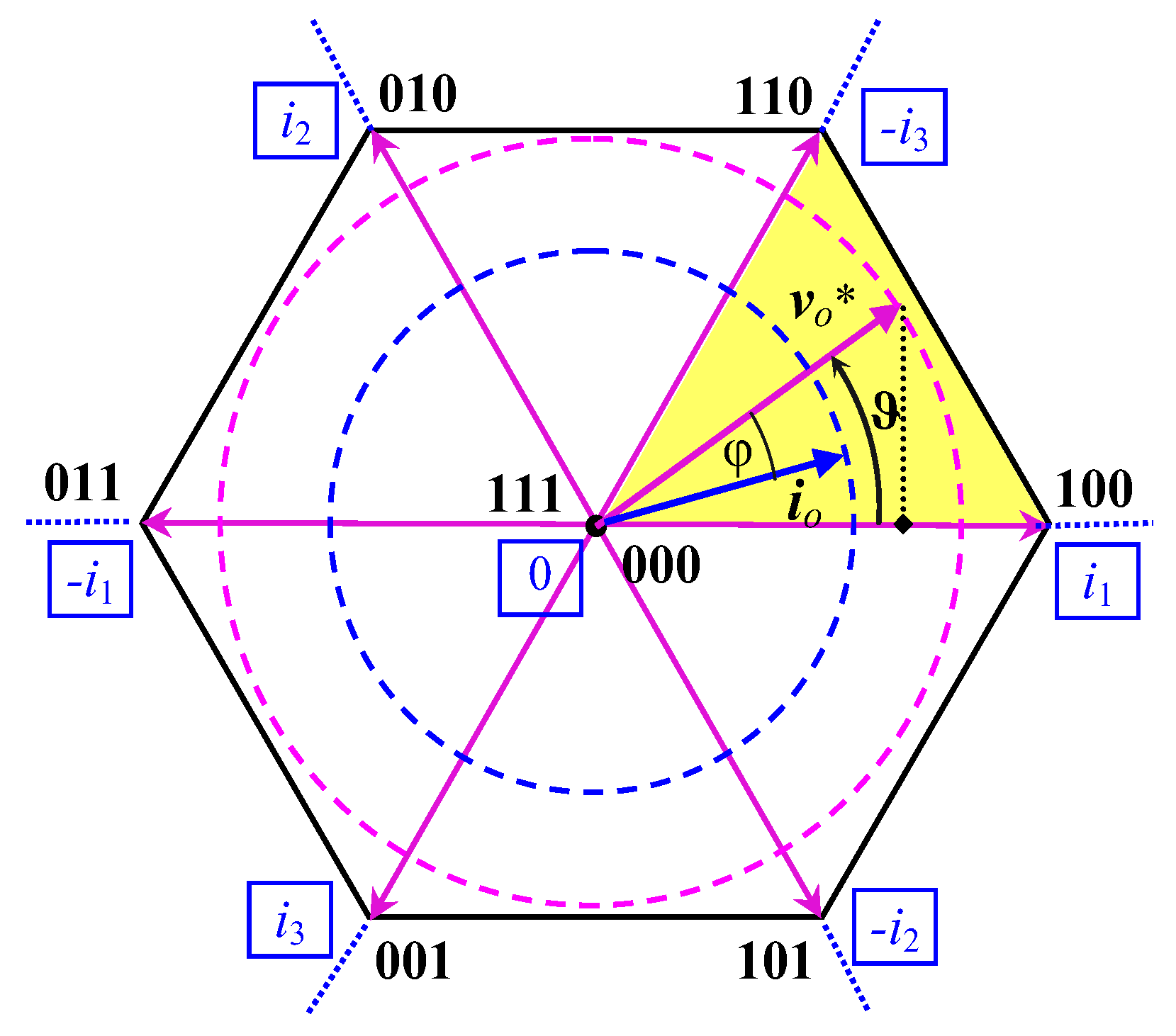
The instantaneous sum of the phase currents according to the Kirchhoff current law (KCL) is null since a three-wire load is considered. Regarding this, there is a direct analogy between the output voltage vector and the value of the input current i(t) (Figure 2).
Finally, the switching frequency input current component can be readily obtained utilizing Equations (3), (4), and (6), as shown in Equation (7):
Due to the symmetry of the inverter input current, the analysis can be limited to one-sixth of the fundament period (T/6 or 60°), that is, the yellow triangle emphasized in Figure 2.
2.3. Space Vector PWM
For three-phase inverters, space vector modulation, which corresponds to carrier-based PWM with a min/max common-mode signal injection, is considered as a nearly optimal modulation for the output current THD. Therefore, in this paper, the dc-link voltage ripple analysis has been developed for SV modulation and implemented with carrier-based PWM by centering the modulating signals.
In the case of sinusoidal balanced reference voltages and by using the definition of the modulation index, the reference voltage space vector can be defined as . There are eight possible switching combinations for a three-phase VSI corresponding to six active and two zero voltage vectors (Figure 2). The reference voltage vector is generated by synthesizing two active and two zero voltage vectors in every switching period Tsw and the volt-second balance is maintained by choosing an appropriate application time for these vectors. In the case of symmetric SV-PWM, it is enough to determine the sequence in one half of the switching period (Tsw/2) since it will be symmetrically repeated in the next half.
The application times of each voltage vector are determined as:
The application time t0 of the null voltage vector is equally shared between the two zero switching states 000 and 111 (centered modulation). The limit of the linear modulation range is m ≤ mmax = 1/, where mmax is given by the generalized expression for k phases mmax = [2 cos(π/2k)]−1, as stated in [23].
3. dc-Link Voltage Ripple Evaluation
3.1. dc-Link Voltage Components
Similar to the inverter input current, the instantaneous dc-link voltage has the following components: the dc (average) component V, the low-frequency component, and the high-frequency component ∆v. The low-frequency component is zero since it is determined on the basis of the corresponding current component that is zero when the load is balanced. Correspondingly, the instantaneous dc-link voltage is expressed as:
The dc component V is simply determined by the supply voltage Vdc and the voltage drop on the dc source resistance R:
The peak-to-peak amplitude ∆vpp of the high-frequency (switching frequency) dc-link voltage ripple component can be defined as the difference between its maximum and minimum value within the switching period:
3.2. Peak-to-Peak Voltage Ripple Evaluation
To determine Δvpp, the input current switching frequency component, circulating through the dc-link capacitor C, has to be estimated first. Assuming that the capacitive reactance 1/ωswC dominates the equivalent dc-link RL impedance (at the switching frequency ωsw = 2πfsw = 2π/Tsw), the whole current component Δi circulates through the dc-link capacitor. In this case, the corresponding dc voltage excursion can be determined by integrating Δi over the specific application time interval tpp, determined by the space vector Equations (8)–(10). An effective simplification is obtained by considering Δi constant (ΔI) within the application time interval, leading to:
Due to the inverter input current periodicity i(t), the evaluation of the voltage ripple can be reduced to the phase angle range 0 ≤ ≤ 60°, that is, the first sector of the space vector diagram (Figure 2). Within the first sector, depending on the value of Idc, two different cases can be distinguished according to Figure 3. The actual peak-to-peak dc-link voltage ripple amplitude ∆vpp can be obtained by merging the results corresponding to these two cases.
3.2.1. Case A—Evaluation in the Range i1 ≥ Idc
The dc-link voltage ripple ∆v and its peak-to-peak value ∆vpp are depicted in Figure 3, together with the instantaneous input current i(t). According to Figure 3 (left) and considering the application interval tpp = t0 (bold pink trace), the peak-to-peak voltage ripple can be written on the basis of Equation (14) as
Introducing Equations (4) and (10) into Equation (15) leads to
3.2.2. Case B—Evaluation in the Range i1 < Idc
According to Figure 3 (right) and considering the application interval tpp = t0/2 + t1 (bold pink trace), the peak-to-peak voltage ripple can be written on the basis of Equation (14) as:
Introducing Equations (4), (8), and (10) in Equation (17) leads to
3.2.3. Merging Cases A and B
The actual peak-to-peak dc-link voltage ripple amplitude ∆vpp is obtained by merging the results corresponding to cases A and B:
Finally, from Equation (19), one can see that the magnitude of the dc-link voltage ripple is always determined by the maximum value of those two.
The dc-link peak-to-peak voltage ripple amplitude can be normalized according to:
Applying Equation (20) to both cases A and B (Equations (16) and (18), respectively), the normalized peak-to-peak voltage ripple amplitude is given by:
being
3.3. Maximum Peak-to-Peak Voltage Ripple
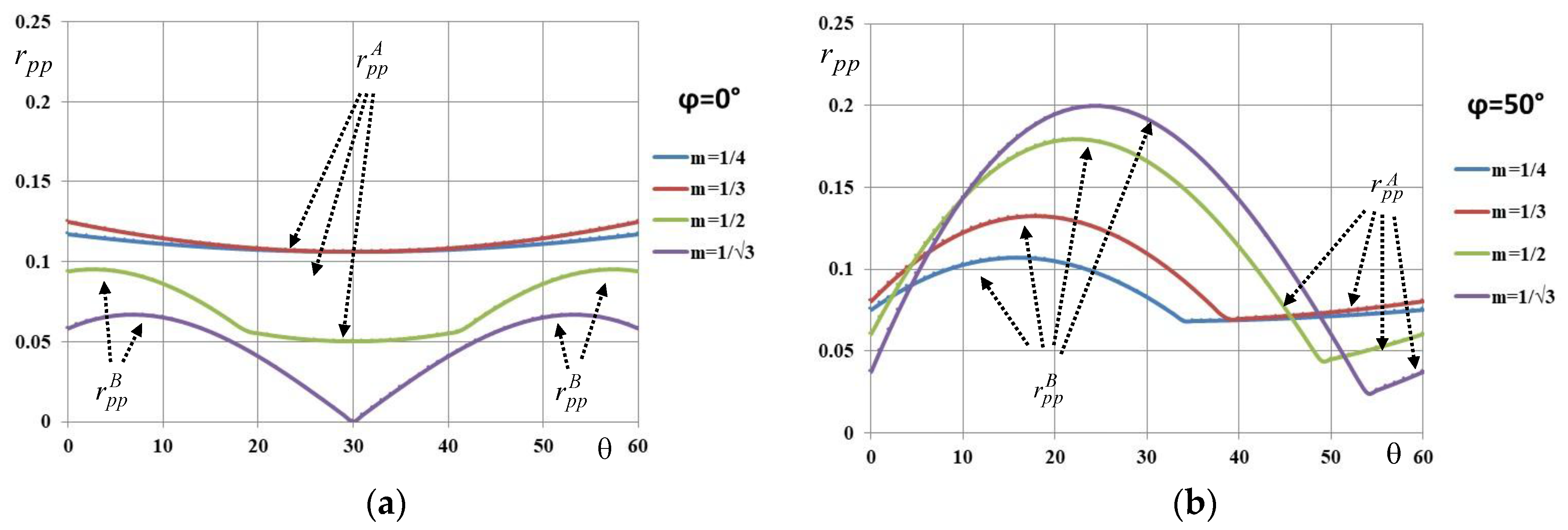
Figure 4 depicts the normalized peak-to-peak voltage switching ripple amplitude calculated by Equation (21) in the phase range = [0, 60°]. Four modulation indices (m = 1/4, 1/3, 1/2, and 1/) and two output phase angles (= 0 and = 50°) have been considered. These cases will be considered also with both numerical and experimental tests in Section 5.
It is noteworthy that the normalized voltage ripple amplitude rpp(ϑ) has a wide excursion, generally ranging between 0 and 0.25, with higher values corresponding to the higher load phase angles. The maximum of the normalized peak-to-peak voltage switching ripple amplitude (Equation (21)) is obtained as a function of the modulation index over the period = [0, 60°]. Different traces are depicted in Figure 5 considering different output phase angles.
For both output phase angles = 0 and = 90°, the maximum has been analytically determined on the basis of Equation (23) as:
For other values of output phase angles ( = 50° and = 30°), the maximum is obtained by properly interpolating data with a reasonable degree of approximation. The following equations are obtained:
4. Guidelines for Designing the dc-Link Capacitor
The dc-link voltage switching ripple has been investigated in previous sections. Based on the proposed calculation method of the dc-link voltage ripple envelope, simple analytical expressions for designing the dc-link capacitor can be obtained. Referring to the switching frequency in the order of kilohertz (kHz), the RL dc source impedance is much higher than the capacitive reactance. It means that only the size of the dc-link capacitor determines the amplitude of the voltage switching ripple.
To achieve a good compromise between the capacitor size and the dc-voltage ripple, the following analysis has been carried out. Two cases of output phase angles are examined. The first case ( = 0) corresponds to most grid-connected applications (no reactive power). The second case ( = 90°) has the highest peak-to-peak voltage ripple and, hence, it requires the biggest dc-link capacitor.
Observing Figure 5 and concerning the case = 0, the following simplification is made:
The dc-link capacitance can be easily calculated from Equation (28) as
In the case of = 90°, is directly proportional to the value of modulation index m. By observing Figure 5 and by considering the maximum value of modulation index (mmax = 0.577), the following simplification is introduced:
Based on Equation (30), the following equation for calculating the dc-link capacitor is proposed:
5. Numerical and Experimental Results
Numerical simulations have been carried out by MATLAB/Simulink (R2016b, MathWorks, Natick, MA, USA) and corresponding experimental tests have been performed in the laboratory by a custom-made inverter prototype.
The three-phase inverter (Figure 1) is controlled by centered PWM (corresponding to SVM) with switching frequency fsw = 2.5 kHz. The simulation circuit parameters summarized in Table 1 are set in order to match the corresponding experimental setup parameters. For the experimental verification, two different output phase angles ( = 0 and = 50°) have been obtained using two different loads.
Figure 6 shows the electrical circuit schematic of the experimental load. The corresponding load parameters presented in Table 2 are estimated by supplying the load by an AC power source/analyzer (50 Hz, three-phase balanced voltage source) and measuring the load currents and voltages.
The whole experimental setup is shown in Figure 7. It consists of a three-phase custom-made VSI using the Mitsubishi PS22A76 intelligent power IGBT module (1200 V, 25 A, Mitsubishi Electric Corporation, Tokyo, Japan), driven by the DSP microcontroller board via an optical interface board. DSP board (TMS320F28379D, Texas Instruments, Dallas, TX, USA) is programmed by Code Composer Studio IDE (CCS) (Texas Instruments, Dallas, TX, USA) with the possibility of real-time adjustment of the modulation parameters by a computer interface.
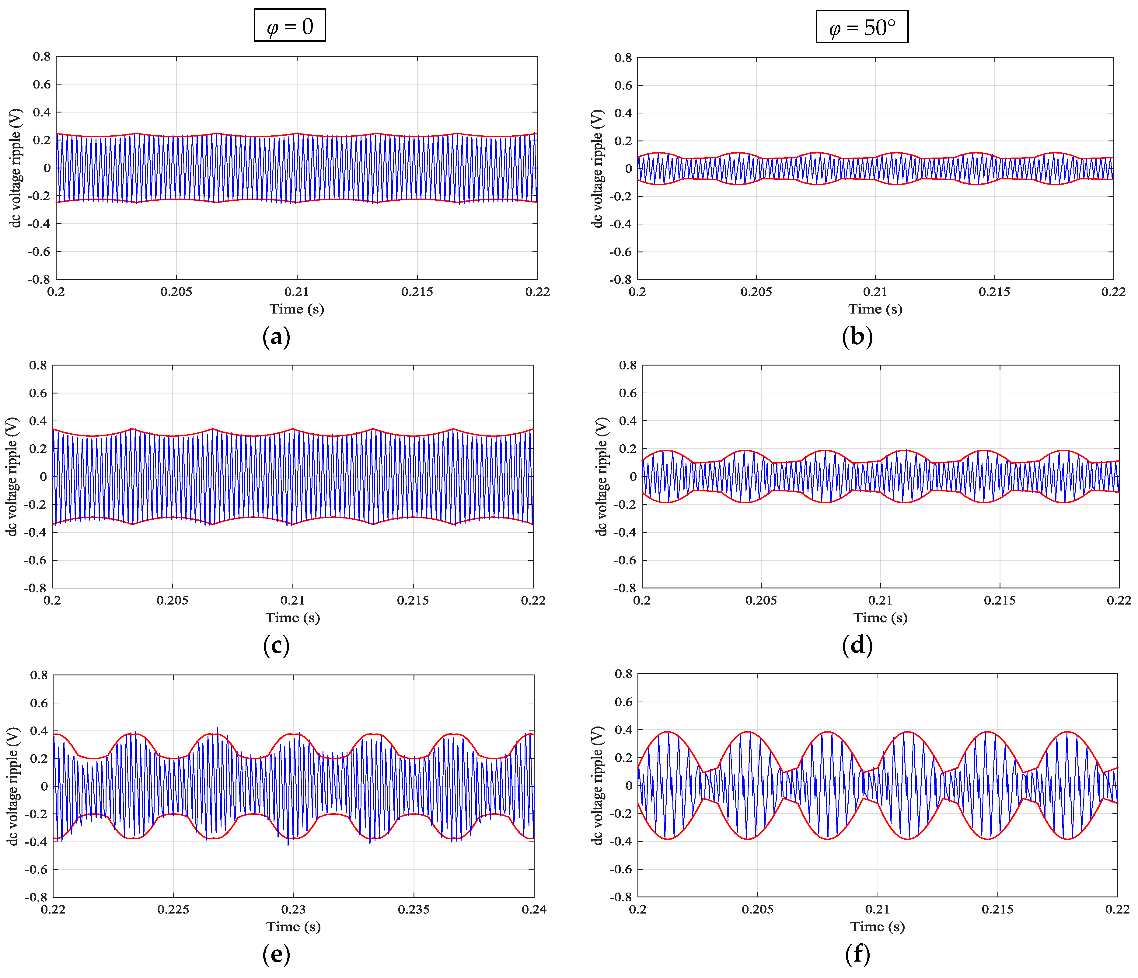
Simulation results are presented in Figure 8. The peak-to-peak envelopes calculated by Equation (19) as the half of peak-to-peak dc-link voltage ripple amplitude ∆vpp/2(t) (red traces) are shown together with the instantaneous dc-link voltage switching ripple ∆v(t) (blue trace) over a fundamental period (T = 20 ms). Two values of the output phase angles = 0 and =50° are considered (left and right column, respectively) and four values of the modulation index (m = 0.25, 0.33, 0.5 and 0.577; from top to bottom) to cover the whole modulation range.
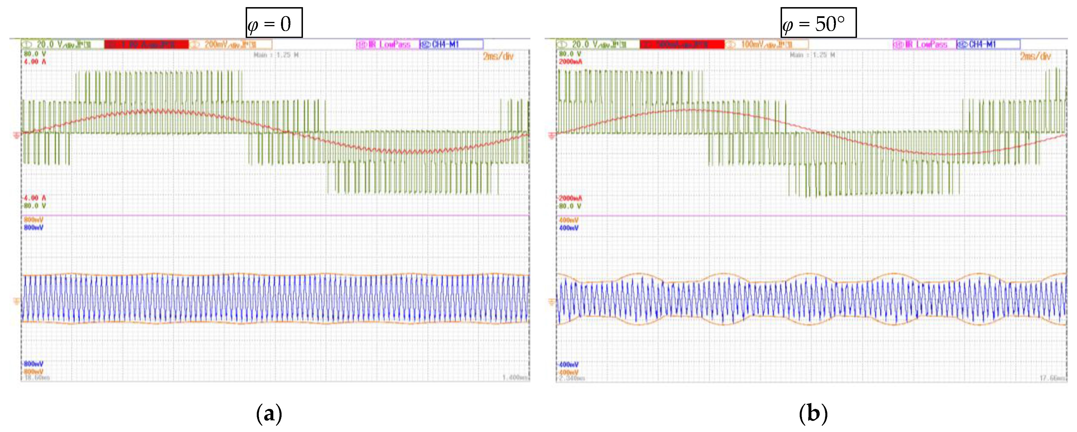
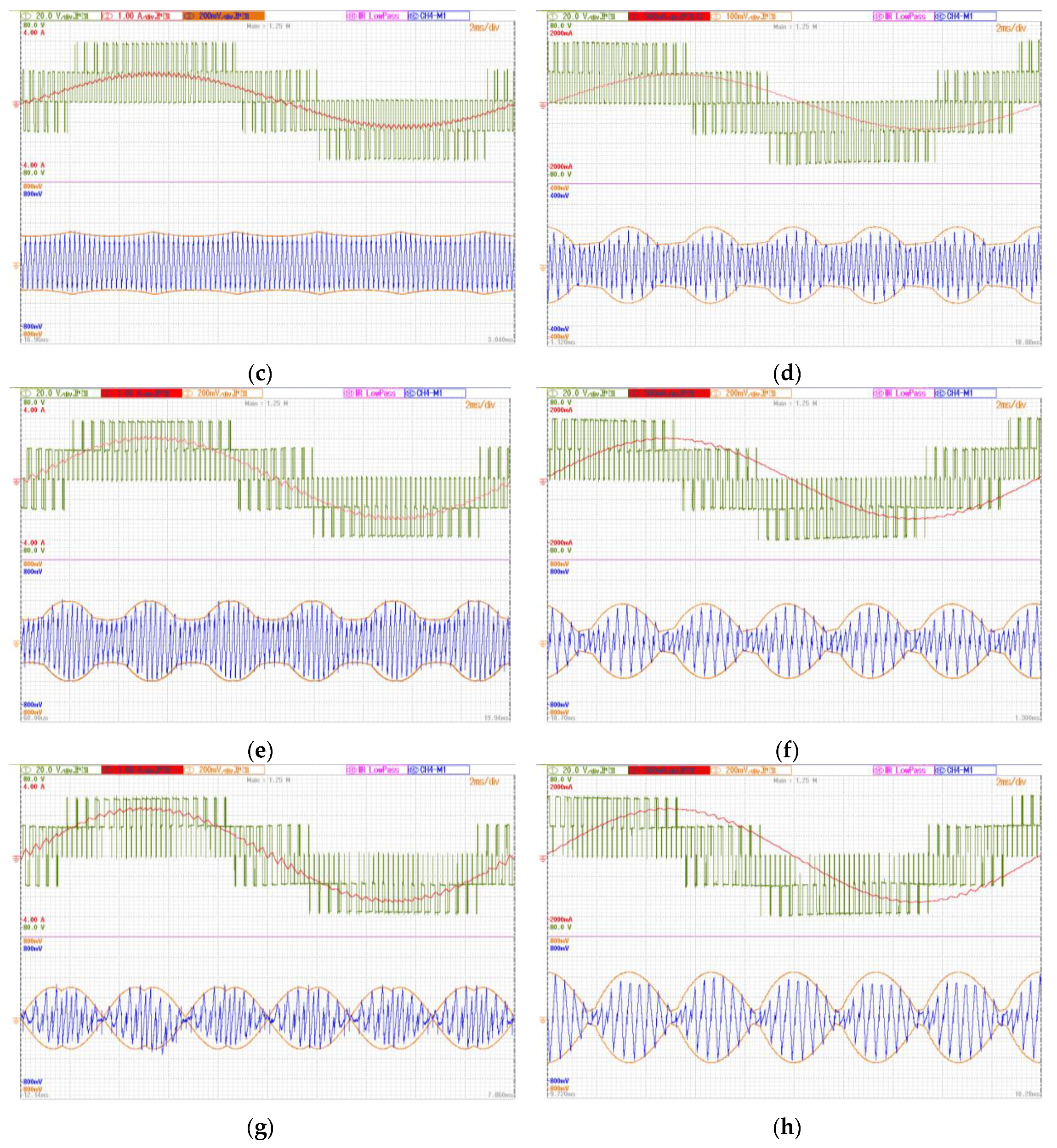
Experimental results are shown by Yokogawa DLM 2024 oscilloscope screenshots (Yokogawa Electric Corporation, Tokyo, Japan) collected in Figure 9. Two values of the output phase angles = 0 and =50° have been considered (left and right column, respectively) and four values of the modulation index—m = 0.25, 0.33, 0.5 and 0.577 (from top to bottom)—to cover the whole modulation range, as in the simulations presented in Figure 8. In all screenshots, two upper traces present the load voltage and current (green and red traces, respectively) and the bottom (blue) trace presents the measured dc-link voltage switching ripple ∆v(t). The additional two orange traces present the calculated envelopes of the voltage ripple (∆vpp/2(t)) provided by the DSP board and displayed using DAC block with a proper voltage scaling.
The switching ripple ∆v(t) has been obtained both numerically and experimentally by properly filtering the instantaneous dc-link voltage, according to Equation (11). In the case of the experimental results, the “ac coupling” built-in function of the oscilloscope has been used together with the built-in low-pass filter in order to better clean the waveforms.
Numerically and experimentally obtained results show good matching between the theoretically calculated envelope and peak-to-peak dc-link voltage ripple for all considered cases of modulation indices and output phase angles, proving the effectiveness of the proposed approach.
6. Conclusions
The detailed calculation and comprehensive experimental investigations of the instantaneous dc-link voltage switching ripple in three-phase PWM VSIs have been carried out. Analyses refer to the case of a non-ideal dc voltage source, representing an input inductive filter or photovoltaic dc supply; however, they are also valid in the case of most dc supplies since the dc source impedance at the inverter switching frequency becomes usually much higher than the dc-link capacitor impedance.
Specifically, the peak-to-peak dc voltage ripple is analytically defined as a function of the output current amplitude, its phase angle, and the modulation index over the fundamental period. In addition, simplified equations to evaluate the maximum value of the peak-to-peak dc-link voltage ripple amplitude in the fundamental period have been derived for different output phase angles. The analysis was carried out for a balanced three-phase system, representing both motor-load and grid-connected applications well. Simple and effective expressions for the dc-link capacitor design have been proposed based on the desired maximum dc-link voltage switching ripple amplitude.
The analytical developments have been verified, both numerically and experimentally, for different values of modulation indices and two output phase angles = 0 (corresponding to most grid-connected inverters) and = 50°. For all considered cases, the correlation between analytical, simulation, and experimental results is very good, which proves the accuracy and effectiveness of the presented developments.
Author Contributions
Marija Vujacic composed the manuscript, performed the simulations and together with Manel Hammami developed the analytical calculations. Milan Srndovic supported the experimental tests and the arrangement of the results. Gabriele Grandi supervised the working group and addressed the research activities.
Conflicts of Interest
The authors declare no conflict of interest.
References
- Holmes, G.D.; Lipo, T.A. Pulse Width Modulation for Power Converters: Principles and Practice; IEEE Series on Power Engineering; John Wiley and Sons: Piscataway, NJ, USA, 2003. [Google Scholar]
- Hava, A.M.; Kerkman, R.J.; Lipo, T.A. Carrier-based PWM-VSI overmodulation strategies: Analysis, comparison, and design. IEEE Trans. Power Electron. 1998, 13, 674–689. [Google Scholar] [CrossRef]
- Broeck, H.V.D.; Skudelny, H.C.; Stanke, G.V. Analysis and Realization of a Pulsewidth Modulator Based on Voltage Space Vectors. IEEE Trans. Ind. Appl. 1988, 24, 142–150. [Google Scholar] [CrossRef]
- Grandi, G.; Loncarski, J. Evaluation of current ripple amplitude in three-phase PWM voltage source inverters. In Proceedings of the 8th IEEE Conference on Compatibility and Power Electronics (CPE), Ljubljana, Slovenia, 5–7 June 2013. [Google Scholar]
- Grandi, G.; Loncarski, J.; Dordevic, O. Analysis and comparison of peak-to-peak current ripple in two-level and multilevel PWM inverters. IEEE Trans. Ind. Electron. 2015, 62, 2721–2730. [Google Scholar] [CrossRef]
- Grandi, G.; Loncarski, J.; Rossi, C. Comparison of peak-to-peak current ripple amplitude in multiphase PWM voltage source inverters. In Proceedings of the 15th IEEE Conference on Power Electronics and Applications (EPE), Lille, France, 3–5 September 2013. [Google Scholar]
- Jiang, D.; Wang, F. Current-ripple prediction for three-phase PWM converters. IEEE Trans. Ind. Appl. 2014, 50, 531–538. [Google Scholar] [CrossRef]
- Bierhoff, M.; Brandenburg, H.; Fuchs, F.W. An analysis on switching loss optimized PWM strategies for three-phase PWM voltage source converters. In Proceedings of the 33rd Annual Conference of the IEEE Industrial Electronics Society (IECON), Taipei, Taiwan, 5–8 November 2007. [Google Scholar]
- Vujacic, M.; Srndovic, M.; Hammami, M.; Grandi, G. Evaluation of DC voltage ripple in single-phase H-bridge PWM inverters. In Proceedings of the 42nd Conference of the IEEE Industrial Electronics Society (IECON), Florence, Italy, 24–27 October 2016. [Google Scholar]
- Vujacic, M.; Hammami, M.; Srndovic, M.; Grandi, G. Theoretical and experimental investigation of switching ripple in the DC-link voltage of single-phase H-bridge PWM inverters. Energies. 2017, 10, 1189. [Google Scholar] [CrossRef]
- Dahono, P.A.; Sato, Y.; Kataoka, T. Analysis and Minimization of ripple components of input current and voltage of PWM inverters. IEEE Trans. Ind. Appl. 1996, 32, 945–950. [Google Scholar] [CrossRef]
- Gohil, G.; Bede, L.; Teodorescu, R.; Kerekes, T.; Blaabjerg, F. Analytical method to calculate the DC link current stress in voltage source converters. In Proceedings of the IEEE International Conference on Power Electronics, Drives and Energy Systems (PEDES), Mumbai, India, 16–19 December 2014. [Google Scholar]
- Kolar, J.W.; Round, S.D. Analytical calculation of the RMS current stress on the DC-link capacitor of voltage-PMW converter systems. IEE Proc. Electr. Power Appl. 2006, 153, 535–543. [Google Scholar] [CrossRef]
- Renken, F. Analytic calculation of the DC-link capacitor current for pulsed three-phase inverters. In Proceedings of the 11th International Conference on Power Electronics and Motion Control, Riga, Latvia, 2–4 September 2004. [Google Scholar]
- Ayhan, U.; Hava, A.M. Analysis and characterization of DC bus ripple current of two-level inverters using the equivalent centered harmonic approach. In Proceedings of the IEEE Energy Conversion Congress and Exposition (ECCE), Phoenix, AZ, USA, 12–22 September 2011. [Google Scholar]
- Bierhoff, M.H.; Fuchs, F.W. DC-link harmonics of three-phase voltage source converters influenced by the pulsewidth-modulation strategy—An analysis. IEEE Trans. Ind. Electron. 2008, 55, 2085–2092. [Google Scholar] [CrossRef]
- Pei, X.; Zhou, W.; Kang, Y. Analysis and calculation of DC-link current and voltage ripples for three-phase inverter with unbalanced load. IEEE Trans. Ind. Electron. 2015, 30, 5401–5412. [Google Scholar]
- McGrath, B.P.; Holmes, D.G. A general analytical method for calculating inverter DC-link current harmonics. IEEE Trans. Ind. Appl. 2009, 45, 1851–1859. [Google Scholar] [CrossRef]
- Nishizawa, K.; Nagaoka, J.I.; Odaka, A.; Toba, A.; Umida, H. Reduction of input current harmonics based on space vector modulation for three-phase VSI with varied power factor. In Proceedings of the IEEE Energy Conversion Congress and Exposition (ECCE), Milwaukee, WI, USA, 18–22 September 2016. [Google Scholar]
- Hobraiche, J.; Vilain, J.P.; Macret, P.; Patin, N. A New PWM Strategy to Reduce the Inverter Input Current Ripples. IEEE Trans. Power Electron. 2009, 24, 172–180. [Google Scholar] [CrossRef]
- Nguyen, T.D.; Patin, N.; Friedrich, G. Extended Double Carrier PWM Strategy Dedicated to RMS Current Reduction in DC Link Capacitors of Three-Phase Inverters. IEEE Trans. Power Electron. 2014, 29, 396–406. [Google Scholar] [CrossRef]
- Vujacic, M.; Hammami, M.; Srndovic, M.; Grandi, G. Evaluation of DC voltage ripple in three-phase PWM voltage source inverters. In Proceedings of the 26th IEEE International Symposium on Industrial Electronics (ISIE), Edinburgh, UK, 19–21 June 2017. [Google Scholar]
- Levi, E.; Dujic, D.; Jones, M.; Grandi, G. Analytical Determination of DC-bus Utilization Limits in Multi-Phase VSI Supplied AC Drives. IEEE Trans. Ener. Convers. 2008, 2, 433–443. [Google Scholar] [CrossRef]
Figure 1.
Circuit scheme of the three-phase voltage source inverter (VSI) under investigation.
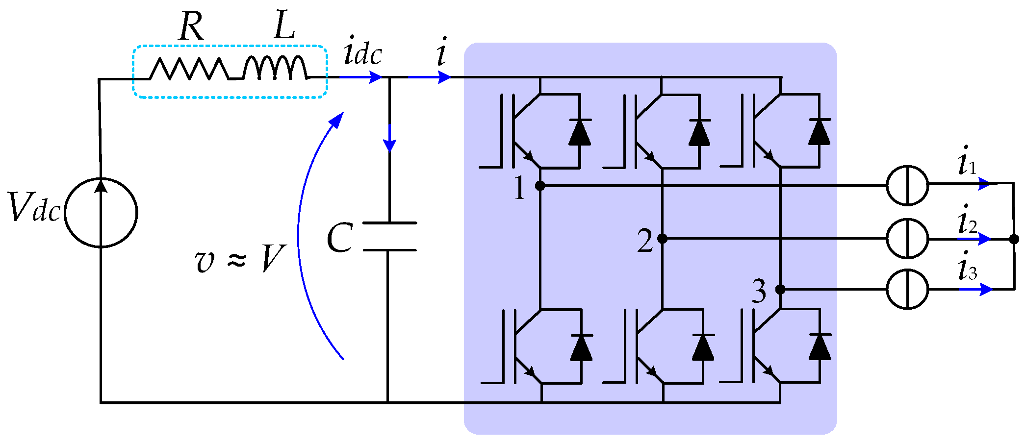
Figure 2.
Space vector diagram of inverter output voltage emphasizing the input dc current (framed) for each inverter state (S1 S2 S3).
Figure 2.
Space vector diagram of inverter output voltage emphasizing the input dc current (framed) for each inverter state (S1 S2 S3).

Figure 3.
dc-link current and voltage ripple in one switching period: (a) Case A (0 ≤ ≤ π/3, i1 ≥ Idc), (b) Case B (0 ≤ ≤ π/3, i1 < Idc).
Figure 3.
dc-link current and voltage ripple in one switching period: (a) Case A (0 ≤ ≤ π/3, i1 ≥ Idc), (b) Case B (0 ≤ ≤ π/3, i1 < Idc).
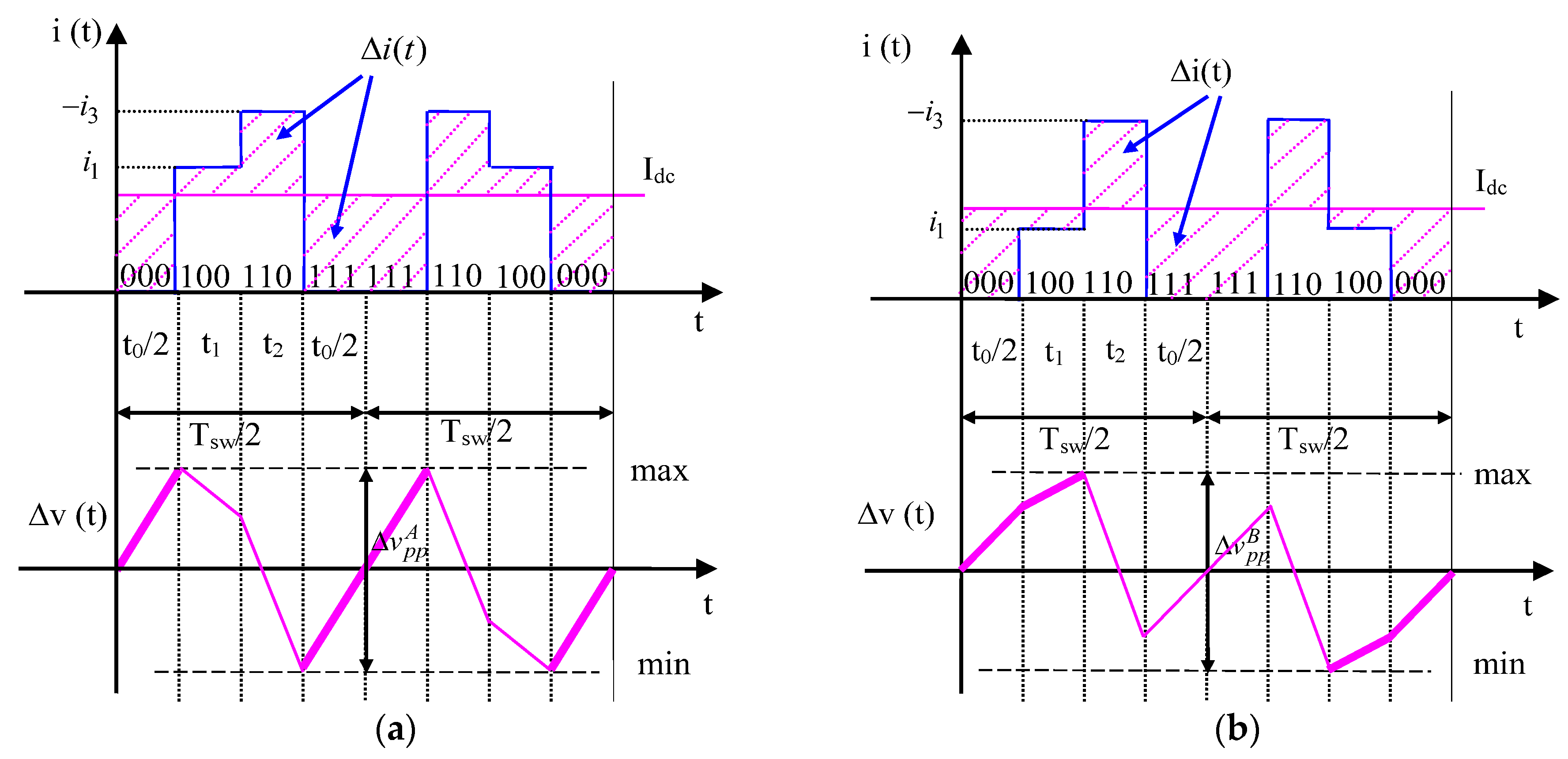
Figure 4.
Normalized peak-to-peak dc-link voltage ripple amplitude rpp() over the period [0, 60°] for different modulation indices, m = 1/4, 1/3, 1/2 and 1/, and output phase angles (a) = 0° and (b) 50°.
Figure 4.
Normalized peak-to-peak dc-link voltage ripple amplitude rpp() over the period [0, 60°] for different modulation indices, m = 1/4, 1/3, 1/2 and 1/, and output phase angles (a) = 0° and (b) 50°.

Figure 5.
Maximum of normalized peak-to-peak voltage ripple amplitude vs. modulation index for different output phase angles.
Figure 5.
Maximum of normalized peak-to-peak voltage ripple amplitude vs. modulation index for different output phase angles.
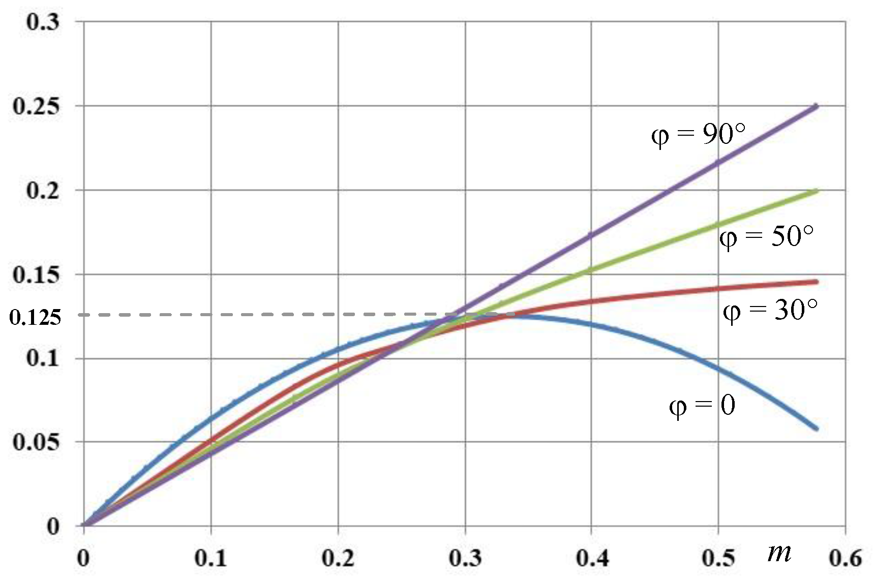
Figure 6.
Three-phase load circuit.
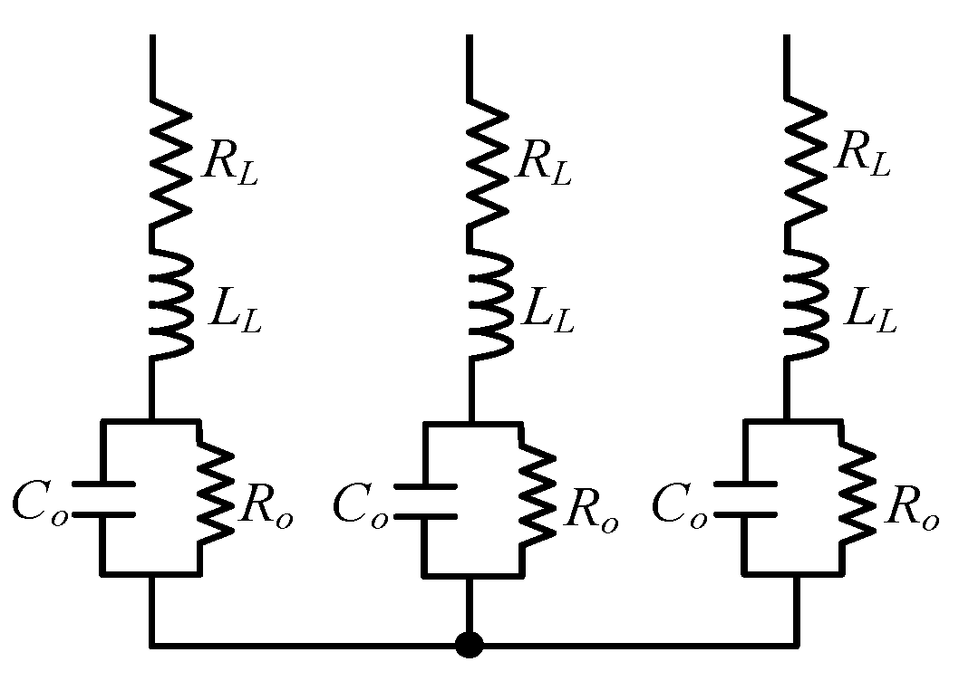
Figure 7.
Experimental setup with a zoom of the three-phase inverter board.
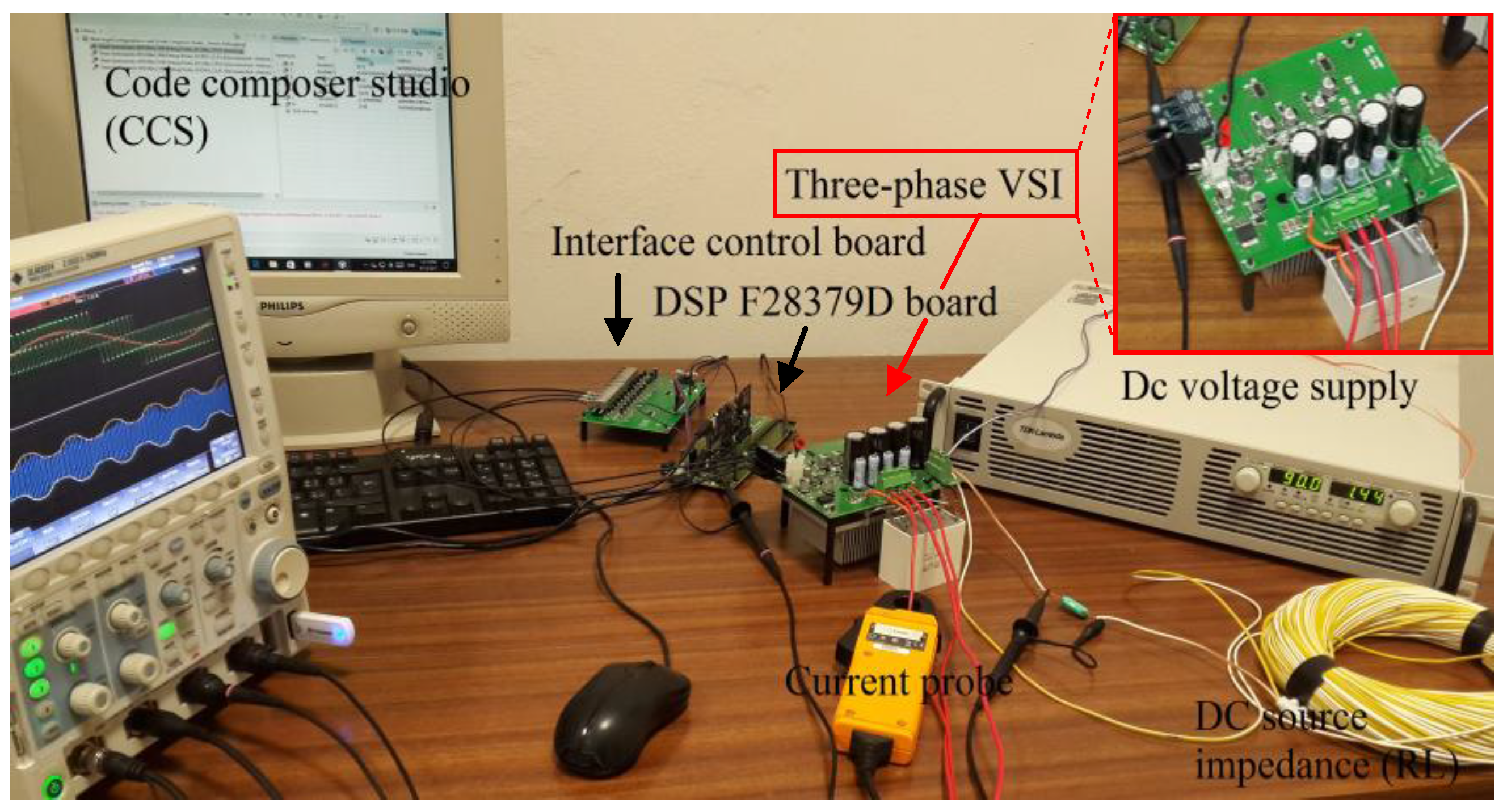
Figure 8.
dc-link voltage switching ripple: simulation results (blue trace) and calculated peak-to- peak envelope (red trace) over a fundamental period for = 0 (left) and = 50° (right), with different modulation indicies: (a,b) m = 0.25; (c,d) m = 0.33; (e,f) m = 0.50; (g,h) m = 0.577.
Figure 8.
dc-link voltage switching ripple: simulation results (blue trace) and calculated peak-to- peak envelope (red trace) over a fundamental period for = 0 (left) and = 50° (right), with different modulation indicies: (a,b) m = 0.25; (c,d) m = 0.33; (e,f) m = 0.50; (g,h) m = 0.577.

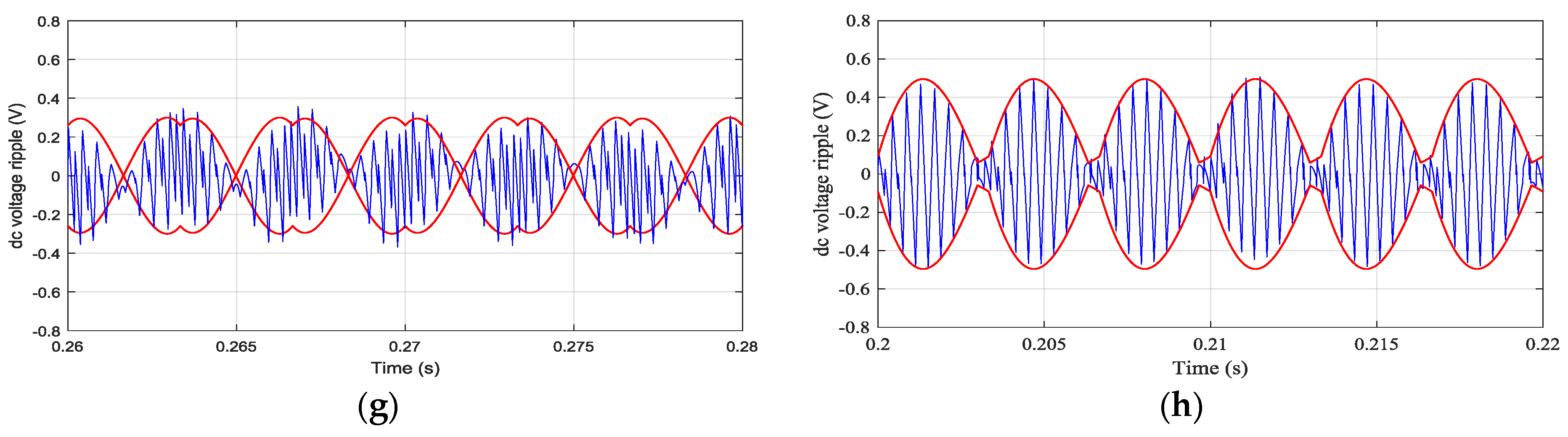
Figure 9.
Experimental results for = 0° (left) and = 50° (right). Upper half: output voltage and current. Lower half: calculated peak-to-peak envelope and measured dc-link voltage switching ripple with different modulation indices: (a,b) m = 0.25; (c,d) m = 0.33; (e,f) m = 0.50; (g,h) m = 0.577.
Figure 9.
Experimental results for = 0° (left) and = 50° (right). Upper half: output voltage and current. Lower half: calculated peak-to-peak envelope and measured dc-link voltage switching ripple with different modulation indices: (a,b) m = 0.25; (c,d) m = 0.33; (e,f) m = 0.50; (g,h) m = 0.577.


Table 1.
Simulation circuit and experimental setup parameters.
| Label | Description | Parameters |
|---|---|---|
| Vdc | dc voltage supply | 90 V |
| R | dc source resistance | 5 Ω |
| L | dc source inductance | 10.15 mH |
| C | dc-link capacitance | 100 μF |
| f | Fundamental frequency | 50 Hz |
| fsw | Switching frequency | 2.5 kHz |
Table 2.
Load parameters.
| Load | φ = 0 | φ = 50° |
|---|---|---|
| RL | 3.16 Ω | 26.8 Ω |
| LL | 20.1 mH | 103 mH |
| Ro | 20 Ω | 0 |
| Co | 58 μF | 0 |
© 2018 by the authors. Licensee MDPI, Basel, Switzerland. This article is an open access article distributed under the terms and conditions of the Creative Commons Attribution (CC BY) license (http://creativecommons.org/licenses/by/4.0/).
Share and Cite
MDPI and ACS Style
Vujacic, M.; Hammami, M.; Srndovic, M.; Grandi, G. Analysis of dc-Link Voltage Switching Ripple in Three-Phase PWM Inverters. Energies 2018, 11, 471. https://doi.org/10.3390/en11020471
AMA Style
Vujacic M, Hammami M, Srndovic M, Grandi G. Analysis of dc-Link Voltage Switching Ripple in Three-Phase PWM Inverters. Energies. 2018; 11(2):471. https://doi.org/10.3390/en11020471
Chicago/Turabian StyleVujacic, Marija, Manel Hammami, Milan Srndovic, and Gabriele Grandi. 2018. "Analysis of dc-Link Voltage Switching Ripple in Three-Phase PWM Inverters" Energies 11, no. 2: 471. https://doi.org/10.3390/en11020471
Note that from the first issue of 2016, this journal uses article numbers instead of page numbers. See further details here.