An Optimized Sensorless Charge Balance Controller Based on a Damped Current Model for Flyback Converter Operating in DCM

1
Harbin Institute of Technology Shenzhen Graduate School; Shenzhen 518055, China
2
Beijing Institute of Spacecraft System Engineering, China Academy of Space Technology, Beijing 100094, China
3
School of Optical and Electronic Information, Huazhong University of Science and Technology, Wuhan 430074, China
*
Author to whom correspondence should be addressed.
Energies 2018, 11(12), 3478; https://doi.org/10.3390/en11123478
Submission received: 16 November 2018
/
Revised: 2 December 2018
/
Accepted: 10 December 2018
/
Published: 13 December 2018
(This article belongs to the Section F: Electrical Engineering)
Abstract
:This paper presents an Optimized Sensorless Charge Balance (OSCB) controller based on a damped current model for flyback converter operating in Discontinuous Conduction Mode (DCM). By solving total differential equations of non-ideal transformer currents, the damped current model is derived with consideration of parasitics, leakage inductance of transformer, and the Resistor-Capacitor-Diode (RCD) snubber circuit. Based on the proposed model, current observation and control algorithms of the Sensorless Charge Balance (SCB) controller are optimized, which forms the OSCB control strategy. The average current damping is considered in the equivalent discrete-time small signal model. Furthermore, frequency analyses show that OSCB controller achieves higher closed-loop bandwidth and lower overshoot than a SCB controller, which indicates an improved transient performance. Finally, both OSCB and conventional SCB controllers are experimentally evaluated on a flyback converter prototype.
1. Introduction
Flyback converters are widely used in industrial applications, since they make it possible to reduce the component count, provide isolation, and achieve good control performance [1,2,3]. The converter can operate in either Continuous Conduction Mode (CCM) or Discontinuous Conduction Mode (DCM), which have different advantages and suit various applications. When the power level is relatively high, flyback converters operating in CCM can achieve higher efficiencies and lower voltage stress than that operating in DCM [4,5]. But this requires high magnetizing inductance and large-size transformer. A flyback converter operating in CCM has limited bandwidth since the transfer function contains a Right Half Plane (RHP) zero. Compared to CCM operation, DCM operation offers many advantages, such as the elimination of turn-ON switching losses and losses associated with reverse recovery of diode, elimination of RHP zero that allows a robust and stable control, and the potential to achieve fast transient response [6]. Since a flyback converter operating in DCM can be considered as a current source that is easy to control, it is widely used in PV-AC module and Power Factor Correction (PFC) systems [7,8,9,10].
In order to improve the performance, different modeling and control strategies are studied for flyback converters [11,12,13]. Current mode control is widely used in power converters owing to its high control loop bandwidth, flexibility for current protection, robustness to disturbances, etc. In power applications, different current mode control strategies are proposed, such as Peak Current Mode (PCM), Valley Current Mode (VCM) and Average Current Mode (ACM) controllers. A practical VCM control strategy is proposed for flyback converters with large duty cycles [14]. This eliminates the need of slope compensation when duty cycle is greater than 50%. Frequency analysis proves that the VCM can achieve similar steady-state and transient response performance to its PCM counterpart. Furthermore, current observation (or estimation) strategies are used for current mode control, which replaces conventional current sensors, and saves cost and power, and reduces the size of the converter system [15,16,17,18,19].
Combined with current observer, Sensorless Charge Balance (SCB) controllers are applied to different converters operating in DCM. This strategy regulates the output voltage by controlling charge current of output capacitor, and it can achieve a fast transient response without current sensing [20,21]. However, non-ideal factors, such as parasitics, leakage inductance of transformer, and snubber circuits, are found to have considerable influences on the closed-loop performance [22,23]. According to [24,25], parasitics can affect the duty cycle of the flyback converter, and cause deviated small-signal models. In order to minimize the influence on the closed-loop control performance, parasitics should be considered in the controller design.
In this paper, an Optimized Sensorless Charge Balance (OSCB) controller based on a damped current model is proposed for flyback converter operating in DCM. With consideration of parasitics, leakage inductance of transformer, and a Resistor-Capacitor-Diode (RCD) snubber circuit, equivalent circuit schemes for the converter are given for switch-on, switch-off, and transform states. Furthermore, total differential equations of non-ideal transformer currents are solved, which provides the damped current model. Based on the proposed model, current observation and control algorithms of a SCB controller are optimized, which forms the OSCB control strategy. The average current damping is considered in the equivalent discrete-time small signal models. Analyses of the small signal models indicate that OSCB controller achieves higher closed-loop bandwidth and lower overshoot than that of SCB controller. Finally, both accuracy of the damped current model and the effectiveness of the OSCB controller are experimentally verified on a flyback converter prototype.
This paper is organized as follows: For better illustrations and comparison, Section 2 provides a basic SCB control strategy and the ideal discrete-time small signal model. In Section 3, equivalent circuit schemes of the converter are given for different states. Based on the schemes, total differential equations of transformer currents are solved with consideration of parasitics, leakage inductance, and the RCD snubber circuit. Furthermore, the OSCB control strategy is derived, while discrete-time small signal model is given with consideration of current damping. In Section 4 and Section 5, simulation and experimental results are given to verify accuracy of the damped current model and effectiveness of OSCB controller. Finally, a brief conclusion is given in Section 6.
2. Sensorless Charge Balance Control for Flyback Converter Operating in DCM
When a flyback converter operates in DCM, its inductor current reaches zero before the end of switching cycle. Since the current is not related to that of previous cycles, the converter can be considered as a controlled current source, which charges the output capacitor and load. Furthermore, sensorless charge balance control can be applied to improve the converter performance. Compared with conventional current mode controllers, the SCB controller greatly improves the transient response by controlling the charge current of output capacitor. Furthermore, the controller eliminates conventional current sensors, since it is based on current observation.
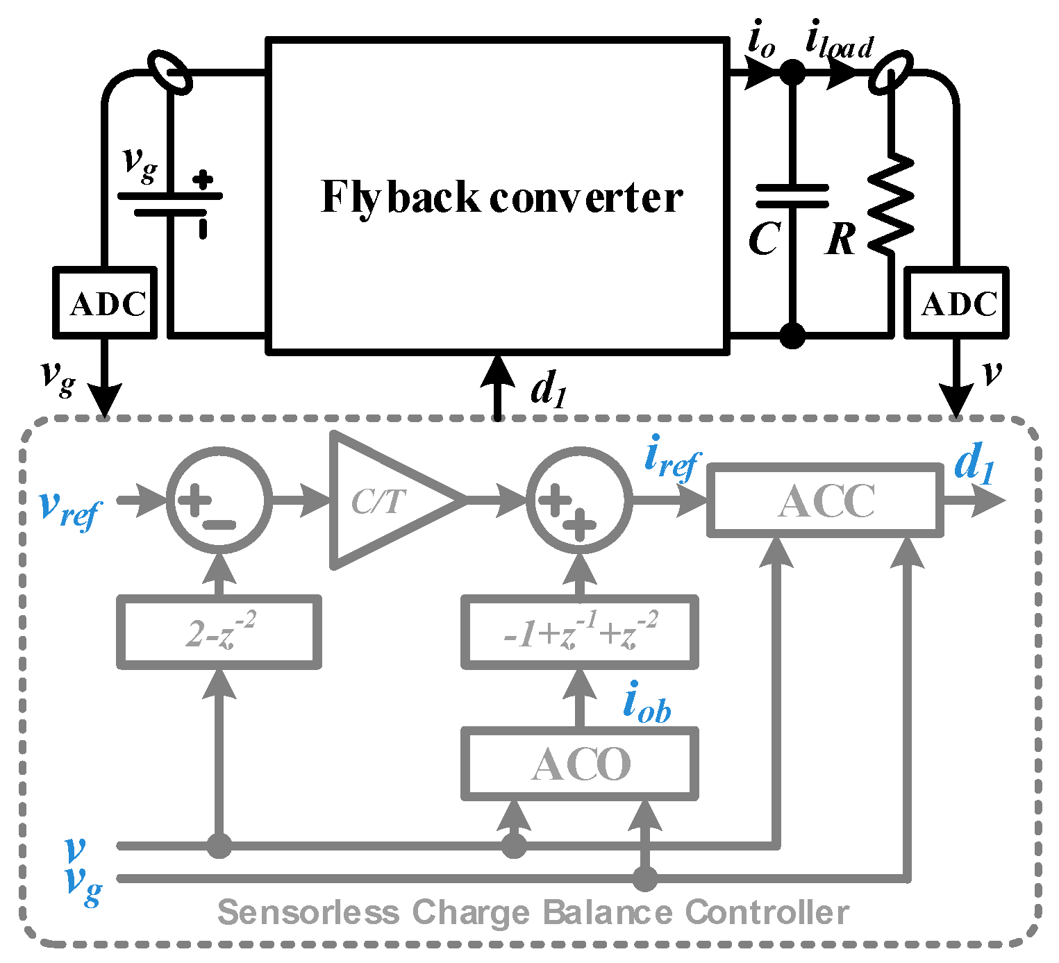
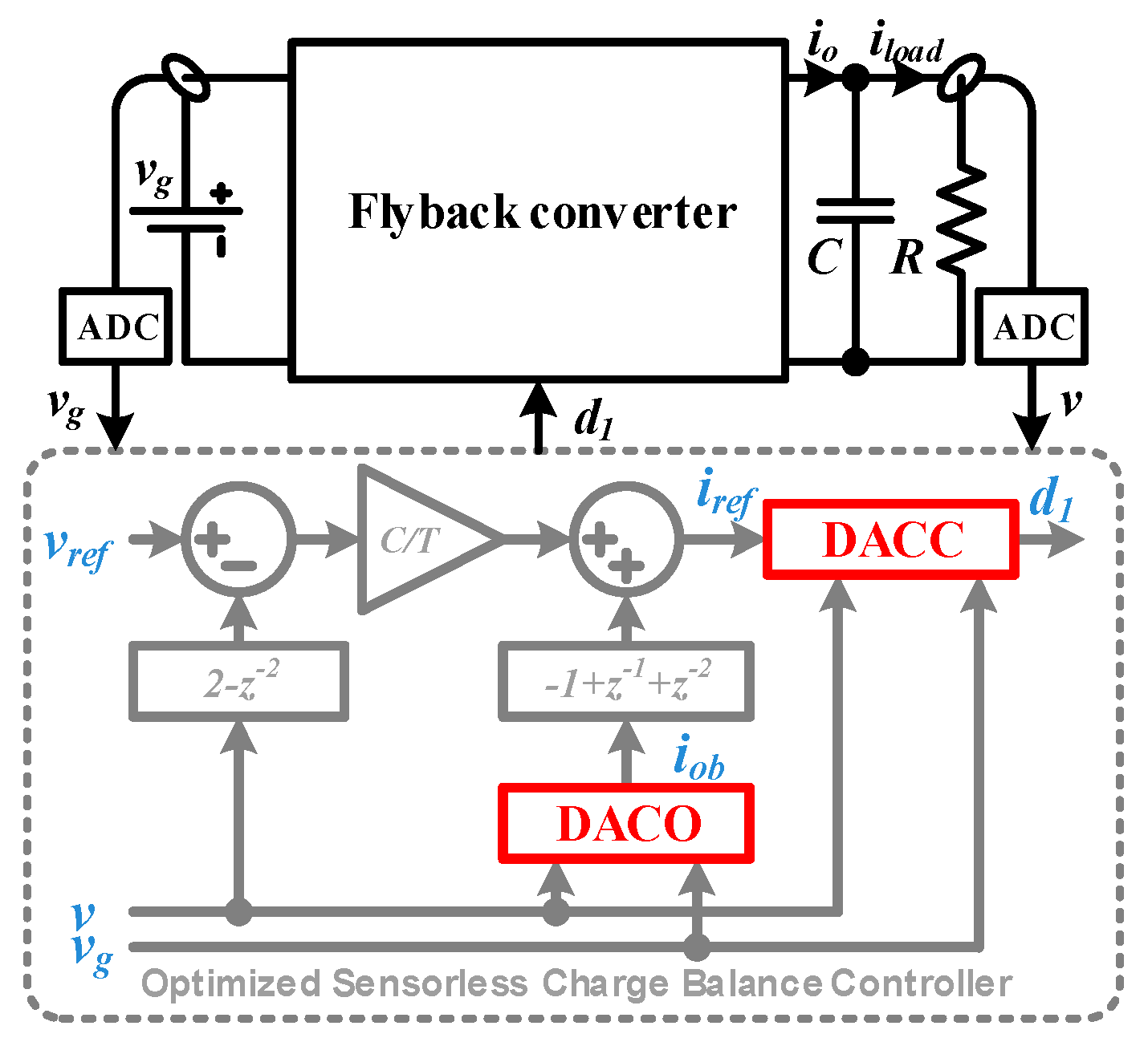
A flyback converter with a SCB controller is given in Figure 1, where d1 is the duty cycle of Digital Pulse Width Modulation (DPWM) signal, C is the output capacitance, R is the load resistance. The SCB controller contains an Average Current Observer (ACO) and an Average Current Controller (ACC). The ACO estimates output current average value and outputs an observed current , while the ACC generates , which makes tracking .
2.1. SCB Control Principle
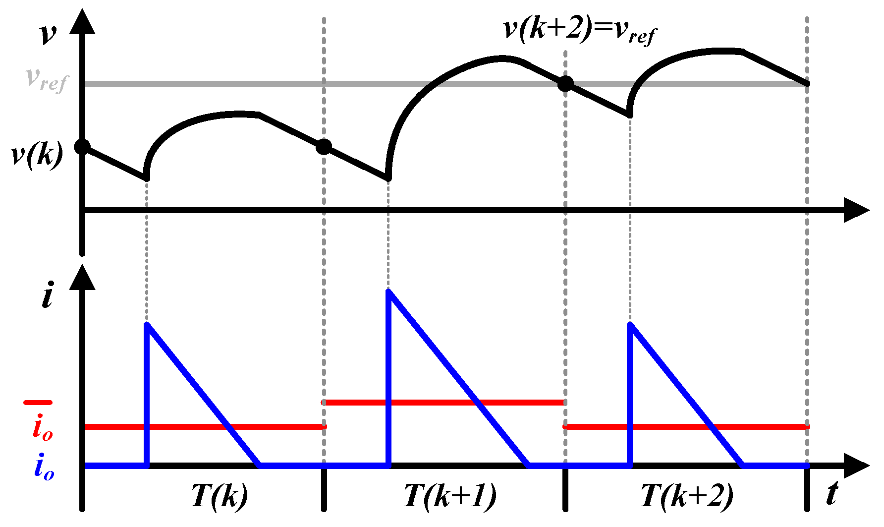
Since and maintains the same at steady state, the output voltage can be controlled by increasing or decreasing , as shown in Figure 2. Supposing that is lower than in the switching cycle, the SCB controller detects the voltage error and increases in the switching cycle. As a result, the output voltage is regulated to at the beginning of switching cycle .
Based on charge balance principle, a reference value for is continuously calculated. Since average charge that flows through output capacitor is , variation of in one switching cycle is given in discrete time domain, as shown in the following
where is substituted by . In order to acquire the control strategy, value of must be calculated from . Therefore, Equation (1) is multiplied by a differential factor , giving
The approximation is made when the switching cycle satisfies , which is valid in most applications. Assuming that tracks in two cycles while tracks in one cycle, substituting and into Equation (2) gives
Although Equation (3) can be used to acquire , it needs for calculation. Sampling for requires current sensors, which increase cost, size and power of the system. It is relatively difficult to carry out the sampling owing to the large current ripple when converter operates in DCM. Therefore, value of is acquired through current observer instead of current sensing. Substituting by gives the final SCB control principle, as shown in Equation (4).
Furthermore, the ACO and ACC algorithms are designed to calculate and . For better illustration and comparison, the basic ACO and ACC algorithms are given in the following subsection.
2.2. Basic ACO and ACC Algorithms and the Ideal Small Signal Model
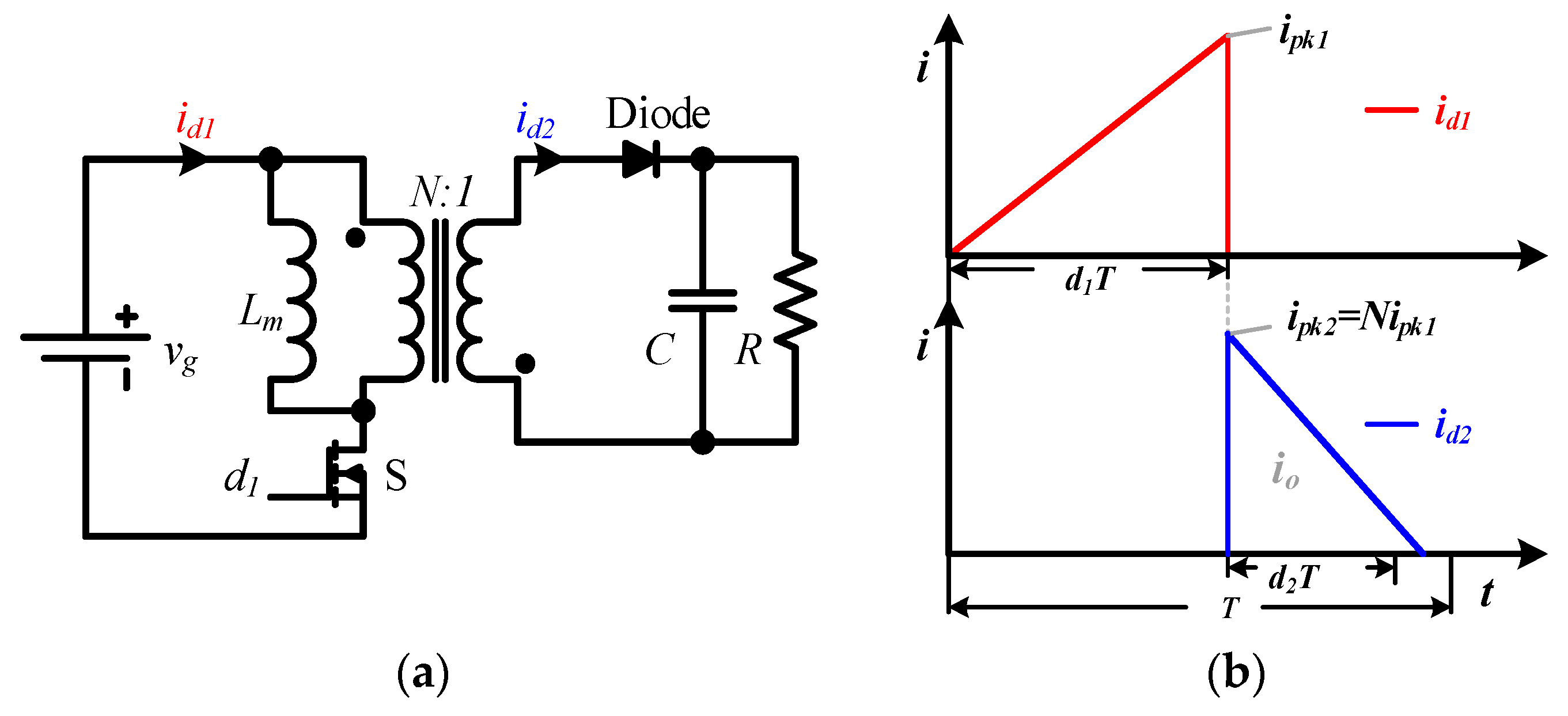
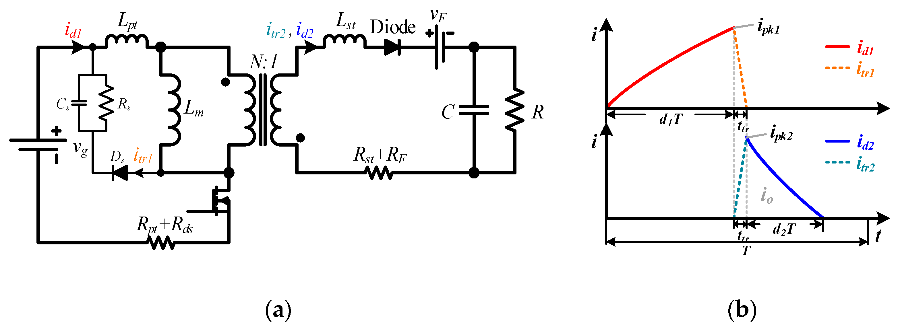
The ACO calculates an observed current value for Equation (4), while ACC outputs a suitable that makes tracking . When operating in DCM, the Flyback converter scheme and its currents are given in Figure 3. A transformer with a turns ratio is utilized. and are transformer currents referred to the primary and secondary sides, respectively.
As many publications have stated, when a flyback converter operates in DCM, the output current can be observed by
To regulate the output current average value as , the duty cycle should be
For an ideal flyback converter, is ensured by Equations (5) and (6). Therefore, a discrete-time small signal model of the closed-loop system is given in Figure 4.
The converter is modelled as a controlled current source that charges the output capacitor and load, and denotes the discrete-time transfer function from output current to output voltage, as shown:
Furthermore, the closed-loop transfer function from to is given by
This function is very close to unity in a wide frequency range, which will be shown by closed-loop simulations in Section 4. Therefore, the output voltage tracks its reference value with a high bandwidth. However, all above calculations are based on the assumption that . When parasitics are considered, this equation is no longer valid, which degrades the system performance.
3. Optimized Sensorless Charge Balance Controller Based on Damped Current Model
The proposed OSCB controller is based on the damped current model, which calculates a more accurate output current than that of conventional model. By solving total differential equations of non-ideal transformer currents, the damped current model is derived with consideration of parasitics, leakage inductance of transformer, and the RCD snubber circuit. Furthermore, current observation and control algorithms of SCB controller are optimized, which forms the OSCB control strategy.
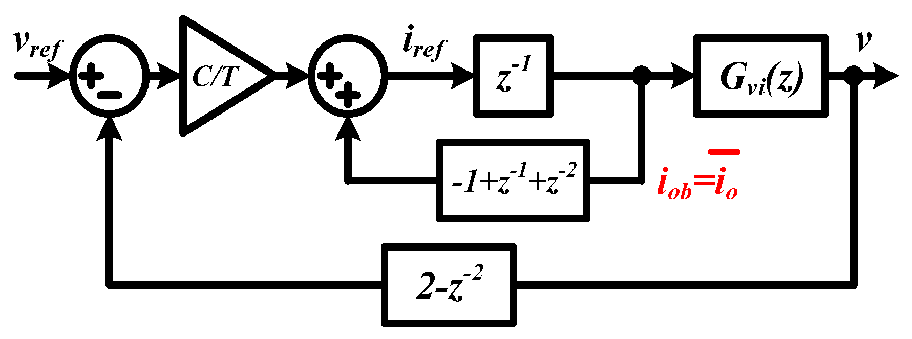
As shown in Figure 5, the OSCB controller has the same control scheme as a conventional SCB controller. The difference lies in the current observation and control algorithms, which are based on the damped current model. In the following, the damped current model is derived by solving total differential equations of multiple states. Based on the current model, the Damped Average Current Observer (DACO) and Damped Average Current Controller (DACC) are acquired. Finally, with consideration of current damping, discrete-time models are derived for system with SCB and OSCB controllers, respectively.
3.1. Damped Current Model Based on Total Differential Equations of Multiple States
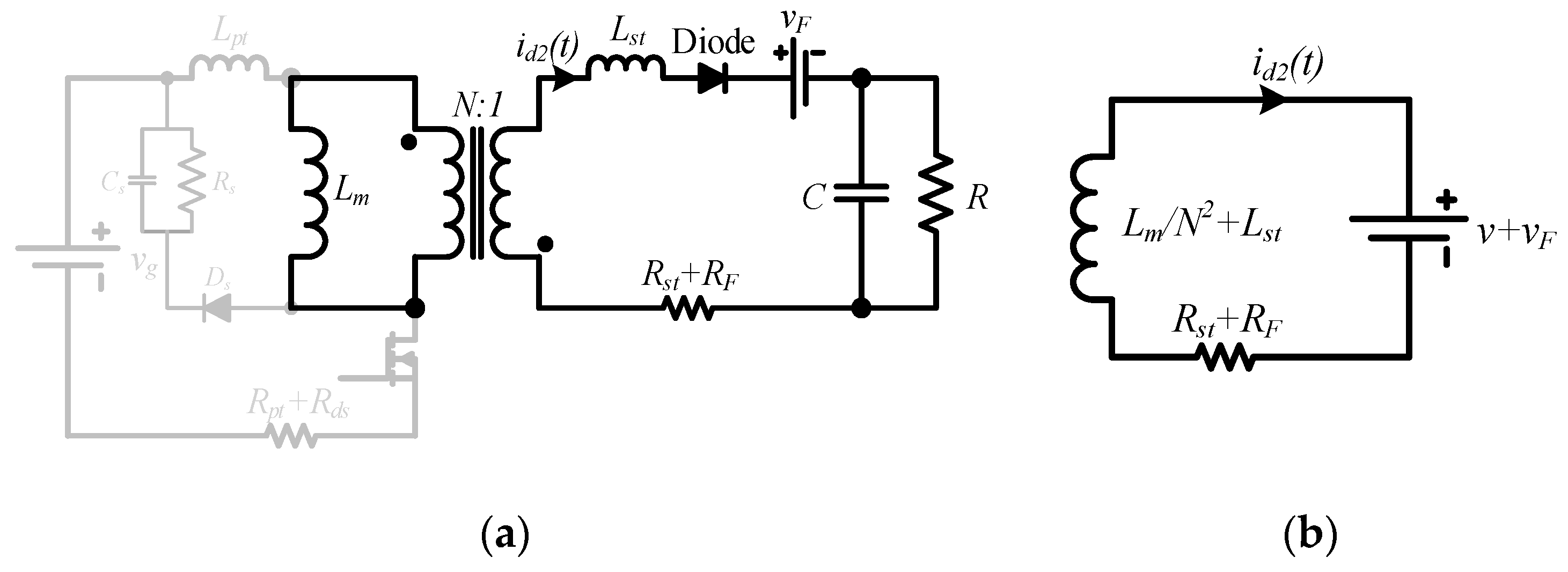
The damped current model is derived with consideration of parasitics, leakage inductance of transformer and RCD snubber circuit. As shown in Figure 6a, and are leakage inductance of transformer primary and secondary sides, and are winding resistances of the primary and secondary sides, is the conduction resistance of transistor, and are conduction resistance and forward voltage of the diode. The RCD snubber circuit, which is formed by {, , }, is used to dissipate the leakage energy and protect the system from surge voltage coming from leakage inductance. Based on this circuit scheme, a damped current model is derived.
Since power loss is induced by parasitics and leakage inductance, ipt and ist are decreased and curved, as shown in Figure 6b. Furthermore, a transform time duration ttr is caused by RCD snubber circuit. In order to simplify analysis, equivalent circuit schemes are given for different states of converter. Furthermore, total differential equations are given for these states, which derive the damped current model.
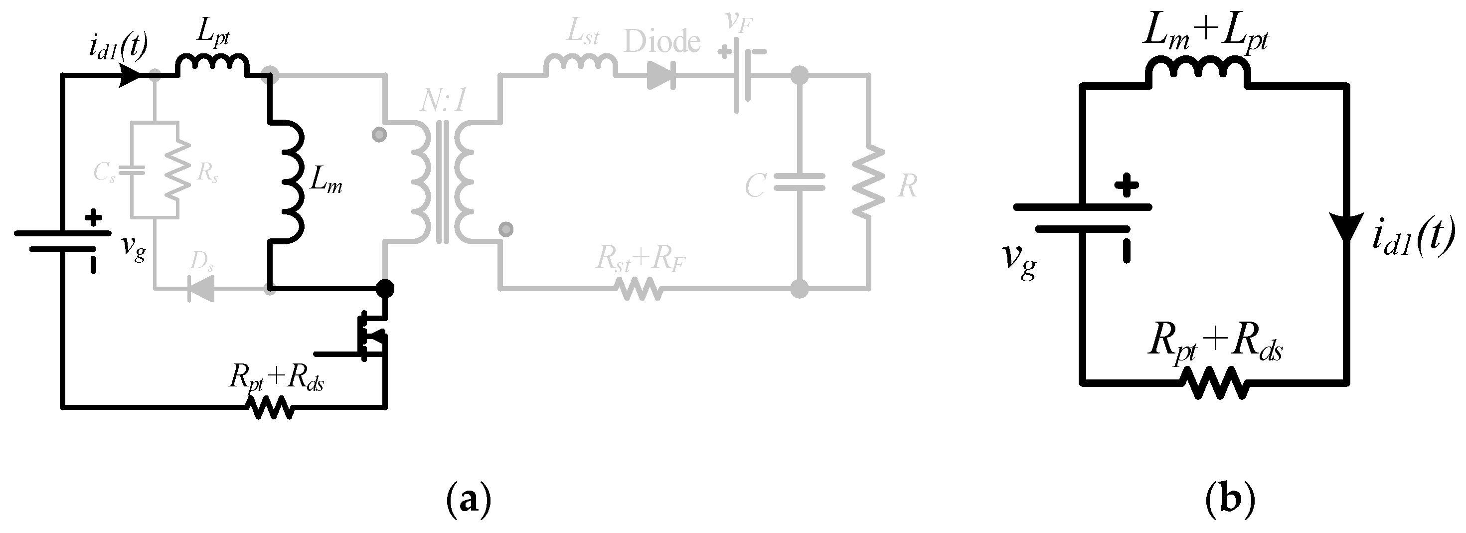
3.1.1. Switch-on State
In switch-on state, currents of the secondary winding and RCD snubber circuit are zero. Therefore, the active circuit and equivalent circuit scheme are given in Figure 7, where denotes the current during .
Since voltage on is in this state, differential equation of is given by
where is derived as
Furthermore, substituting into Equation (10) yields the peak current of primary winding, as shown in the following
This peak current will be used to derive the current of secondary winding.
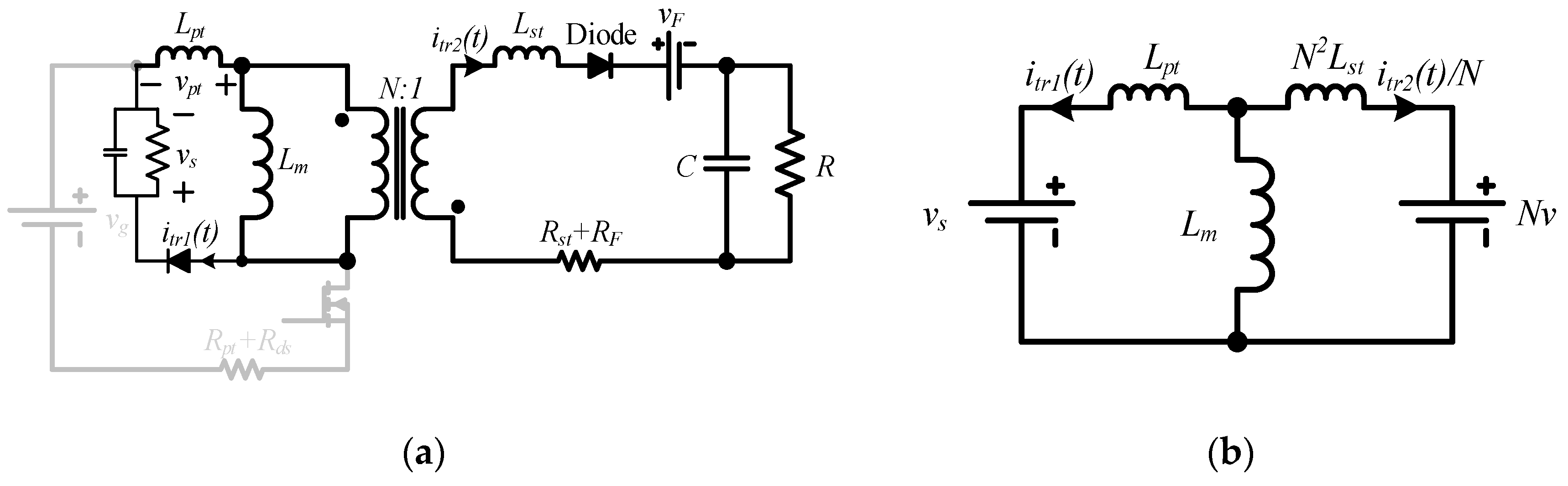
3.1.2. Transform State
In the transform state, there are currents in the primary winding, secondary winding, and RCD snubber circuit. Conventionally, the RCD snubber circuit can be seen as a voltage source . Therefore, the active circuit and equivalent circuit scheme of the converter are given by Figure 8, where and are currents of primary winding and secondary winding, respectively. In order to simplify the analysis, some parasitics are not considered in this state.
Based on the scheme, total differential equation of and is given by
Through integration, relationship between and is given by
Furthermore, peak current of the secondary winding is
In the transform state, the snubber circuit is charged by current of magnetizing inductor. At steady state, the snubber voltage is given by
Based on Figure 8 and linear superposition principle, voltage on is given by
Based on Equations (15) and (16), the transform time duration is derived as
Supposing that rises linearly in the transform state, its contribution to output current average value equals .
3.1.3. Switch-off State
In the off state, currents of the primary winding and RCD snubber circuit are zero. Therefore, the active circuit and equivalent circuit scheme of the converter are given by Figure 9.
The voltage on is , where denotes the non-ideal current during . Therefore, differential equation of is given by
where is solved as
Since , is given by
Furthermore, take output current in the transform state into consideration, the output current average value is solved as
The damped current model calculates a more accurate output current than Equation (5), and it will benefit current mode control strategies that are based on current observation. For the SCB controller, the current observation and control algorithms are optimized, which forms the DACO and DACC.
3.2. DACO and DACC
Based on Equation (21), the DACO and DACC algorithms are given by
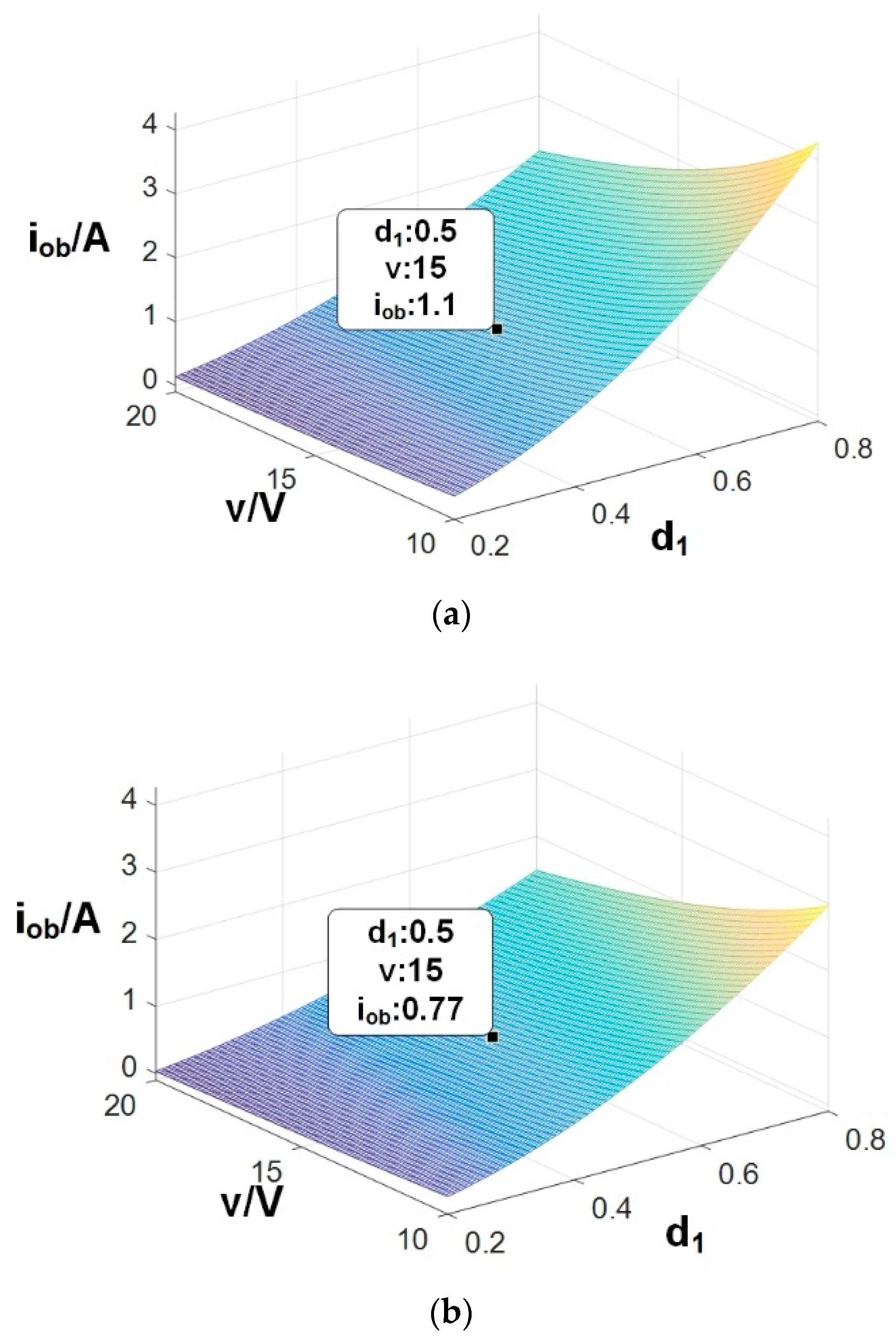
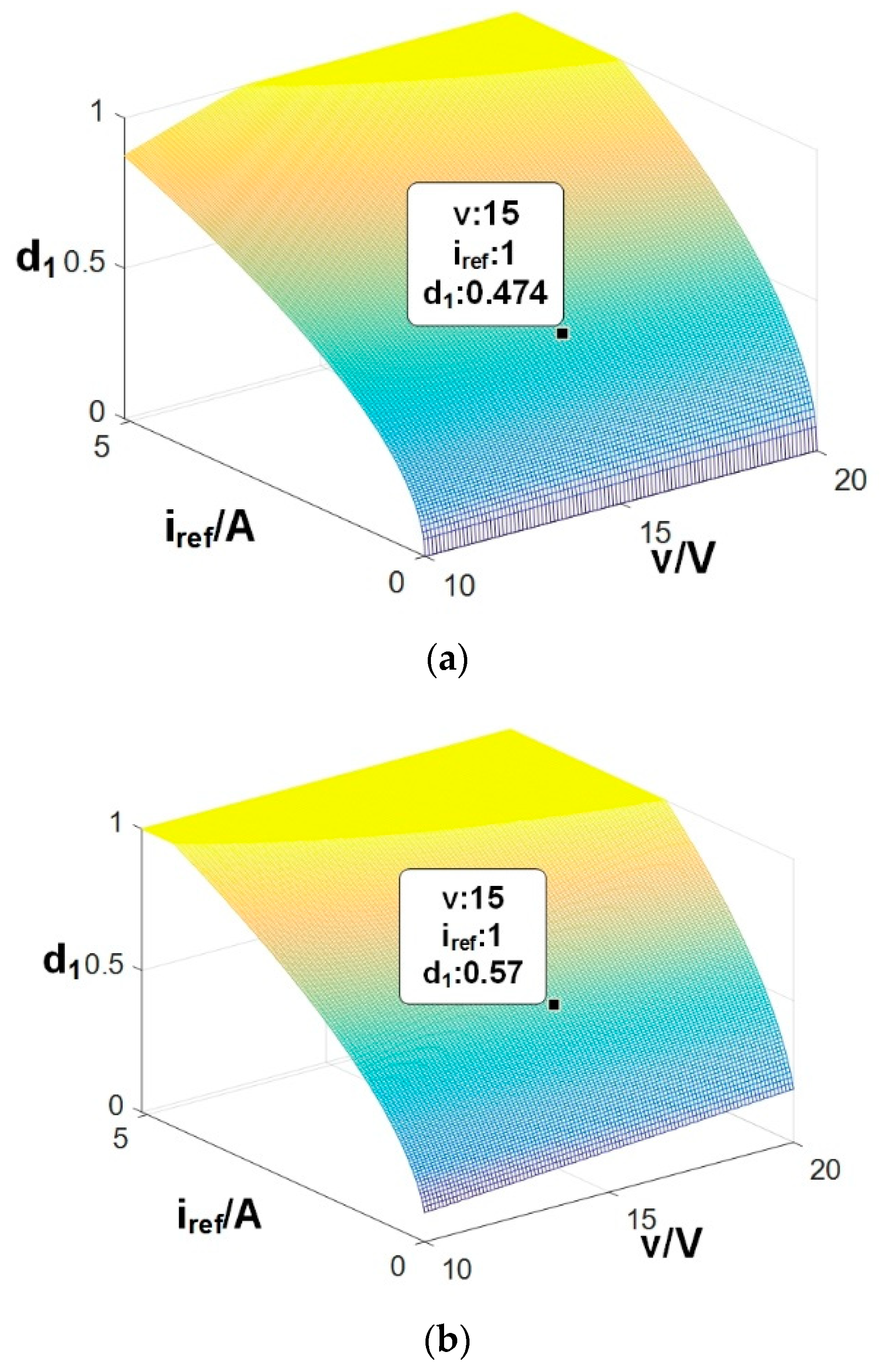
The calculations are relatively complicated. Therefore, they are carried out offline and realized through look-up-table method. With specifications in Section 5, explicit values of and are calculated. When equals 10 V, the results are plotted in Figure 10 and Figure 11.
The DACO calculates a lower output current average value than that of ACO. Taking operation point as an example, the output currents are 1.1 A and 0.77 A, respectively. Therefore, a current damp of exists between the results. The DACC calculates a higher duty cycle than that of ACC. Taking operation point as an example, the calculated duty cycles are 0.474 and 0.57, respectively.
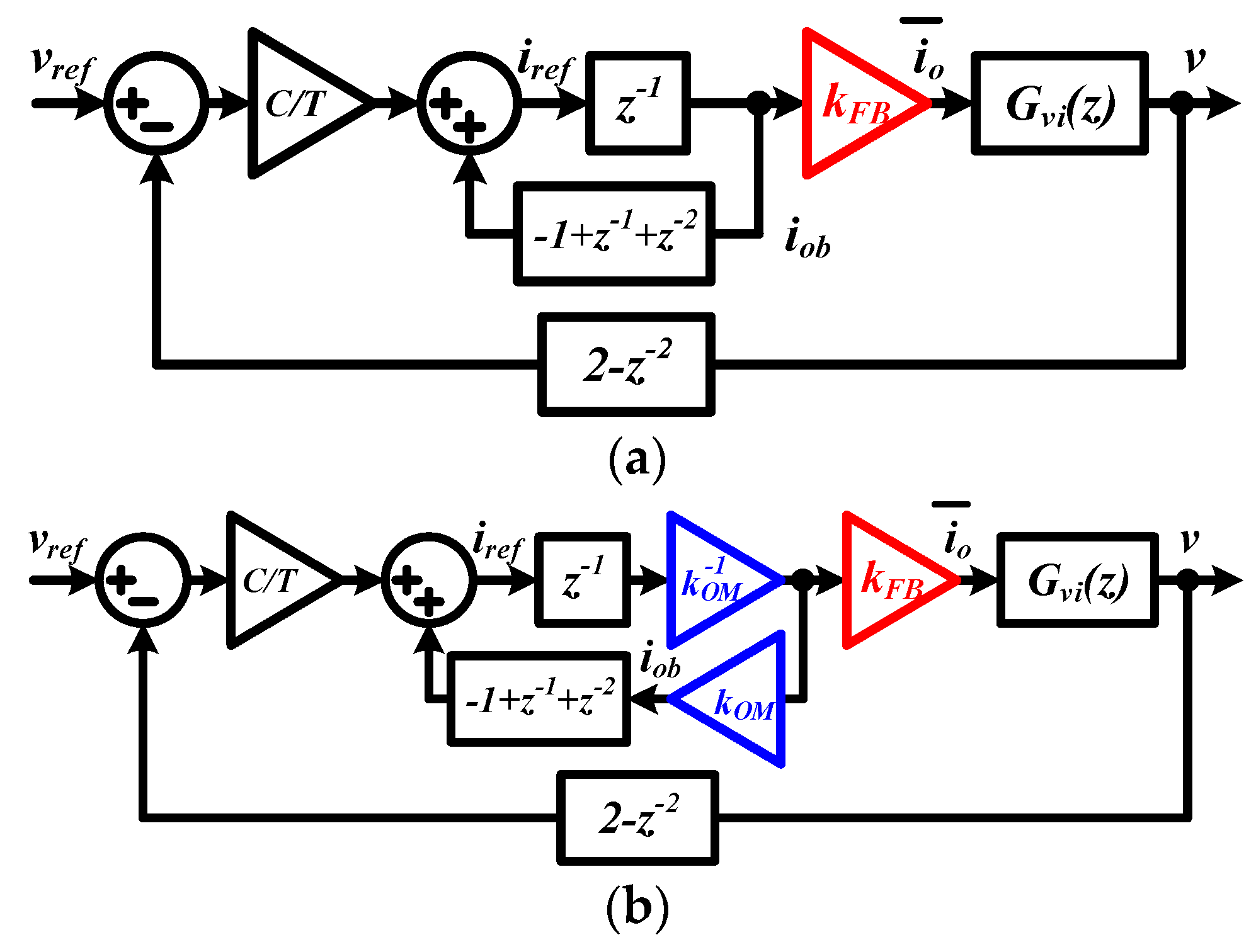
3.3. Discrete-Time Model with Consideration of Current Damping
As shown in the above analysis, the output current average value is decreased by parasitics, leakage inductance of the transformer, and the RCD snubber circuit. In an actual converter system, the damping magnitude might deviate a little from that of the calculations in the damped current model. Therefore, the damping factor is denoted as for actual flyback converter, and for the damped current model. Both and are smaller than unity.
Based on ACO and ACC, exists between the observed current, reference current and actual output current average value, as shown in the following
Based on DACO and DACC, magnitude of the damp is minimized, and the current relationship becomes
Therefore, with consideration of current damping, discrete-time small signal models of the systems are shown in Figure 12.
For converter system with SCB controller, the current gain exists in the system, and the closed-loop transfer function is given by
For converter system with OSCB controller, the equivalent discrete-time model is given in Figure 12b. and the closed-loop transfer function is given by
When , effect of current damping is eliminated, and equals in Equation (8). Therefore, influences of parasitics, leakage inductance of transformer and RCD snubber circuit are eliminated.
4. Simulations
Simulations are carried out by Matlab-simulink to verify effectiveness of the control strategy. Main specifications of the flyback prototype are shown in Table 1. Measured values of parasitics are , , . Parameters of the RCD snubber circuit are , .
Frequency responses of , and are simulated and plotted in Figure 13. The damping factors are set as and , respectively.
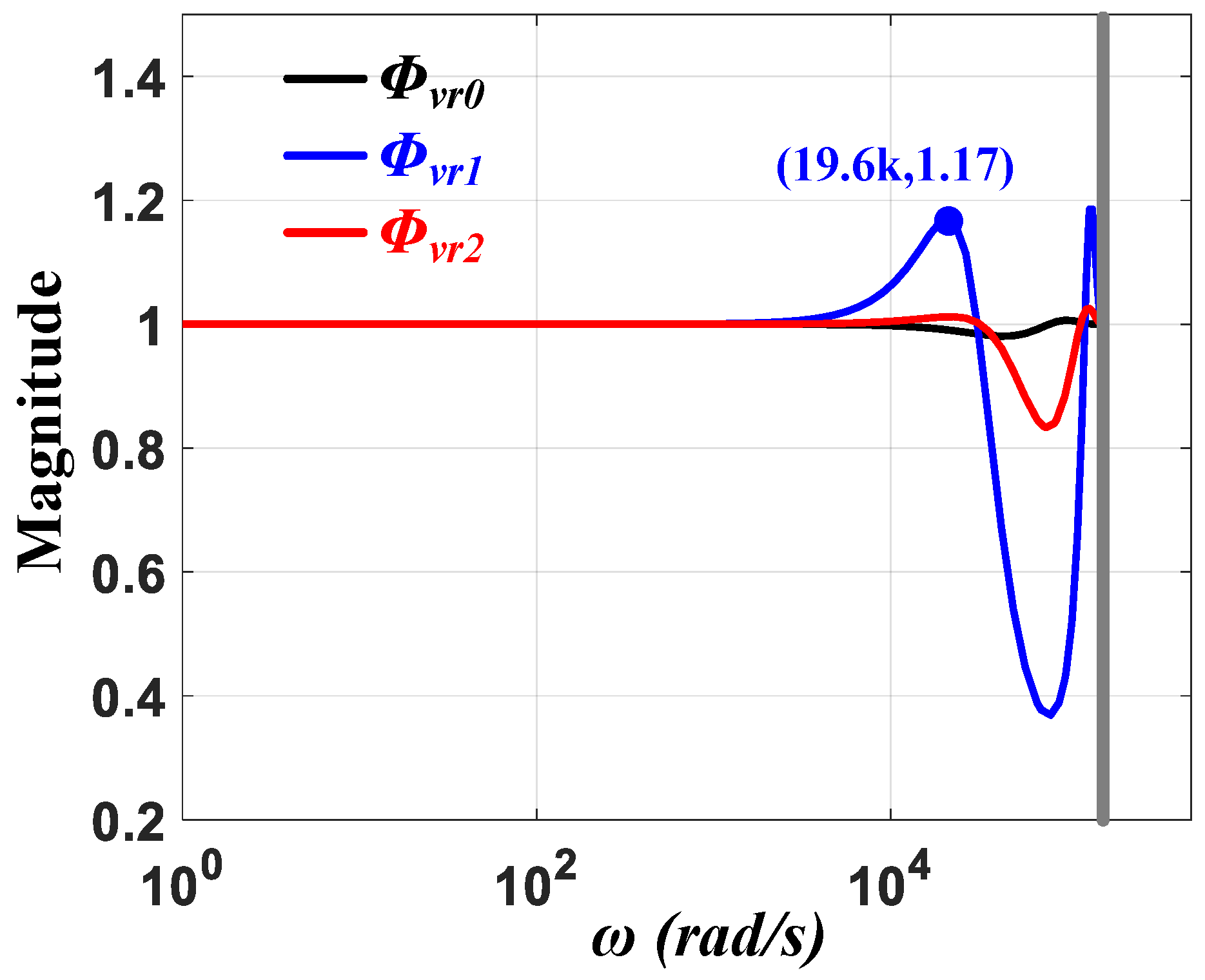
In Figure 13, is the closed-loop transfer function of ideal flyback converter with SCB controller, where current damping is not considered. The magnitude is very close to unity before half of the sampling frequency, which indicates a high bandwidth. With consideration of current damping, the closed-loop transfer function becomes . The frequency response has a spike of 1.17 at 19.6 k rad/s, which indicates overshoot during transient response. The magnitude drop at high frequency indicates a decreased bandwidth. For a converter system with an OSCB controller, the closed-loop transfer function is . Without the spike, the frequency response is much closer to that of . All results prove that OSCB controller achieves higher bandwidth and lower overshoot than the SCB controller.
5. Experiments
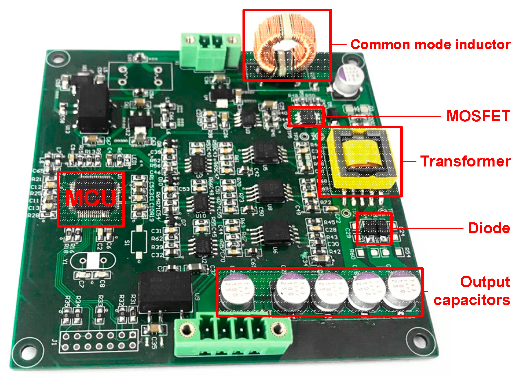
A flyback converter operating in DCM is constructed for the experiments; the prototype is shown in Figure 14. Main specifications and setups are the same as those of the simulations, which used a switching frequency of . A Microcontroller Unit (MCU) tms320f280049 is utilized to implement the digital controller. The MCU is 32 bits, capable of floating-point calculations, and the clock rate is . The main switch is an Infineon IRF7805PbF, which is a N-channel MOSFET (Metal-Oxide-Semiconductor Field-Effect Transistor).
The converter is controlled by SCB and OSCB controllers, respectively. The output current and observed currents are compared to verify accuracy of the damped current model. The output voltages are compared to verify the closed-loop transient responses under SCB and OSCB control.
5.1. Comparison between Observed and Output Currents
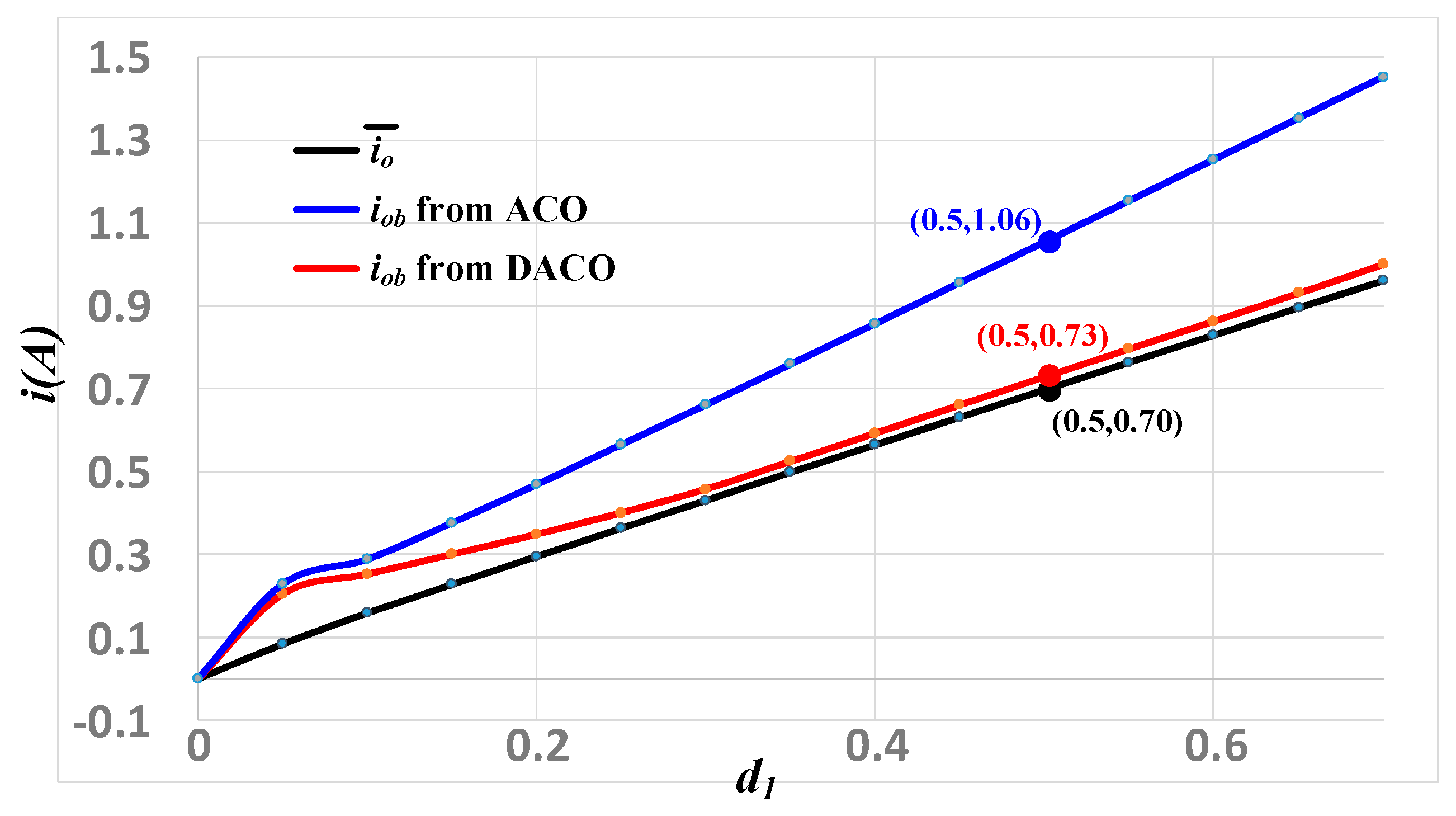
In order to verify accuracy of the damped current model, both outputs of ACO and DACO are compared to the measured output current average value. When duty cycle varies from 0.0 to 0.7, the observed currents and measured current are given in Figure 15.
Both observed currents are higher than the measured average current, which increase along the duty cycle. When the duty cycle is low, both ACO and DACO have relatively large errors. When the duty cycle is higher than 0.2, DACO acquires a more accurate than ACO. Taking as an example, the measured equals 0.70 A, while the observed currents are 1.06 A and 0.73 A from ACO and DACO, respectively. Therefore, relative error of ACO is while relative error of DACO is . The result verifies the accuracy of DACO, which is based on the damped current model.
5.2. Output Voltage Transient Response
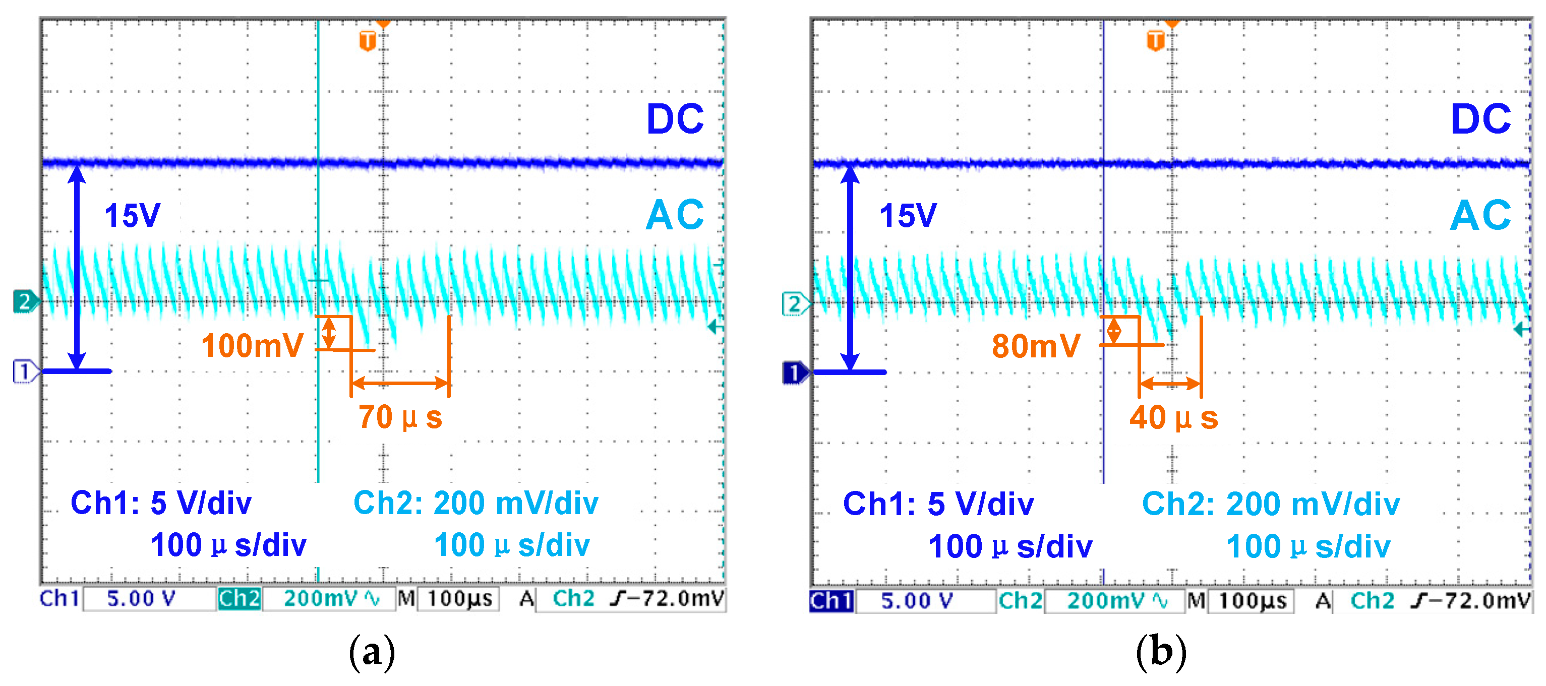
When steps from 10 V to 7.5 V, transient responses of output voltage are given in Figure 16. For flyback converter with SCB controller, high frequency oscillation is found in the transient. The output voltage deviates by 100 mV and re-stabilizes in . With OSCB controller, the output voltage deviates by 80 mV and re-stabilizes in . Therefore, the proposed OSCB controller improves the transient response speed by 43% when the line voltage steps.
When load resistance steps from 50 Ω to 25 Ω, transient responses of output voltage are given in Figure 17. For a converter with a basic SCB controller, the output voltage deviates by 300 mV and re-stabilizes in 20 μs. An overshoot of 50 mV is found in the transient. With the OSCB controller, the output voltage deviates by 200 mV and re-stabilizes in 60 μs. Therefore, the proposed OSCB controller improves the transient response speed by 50% when the load steps.
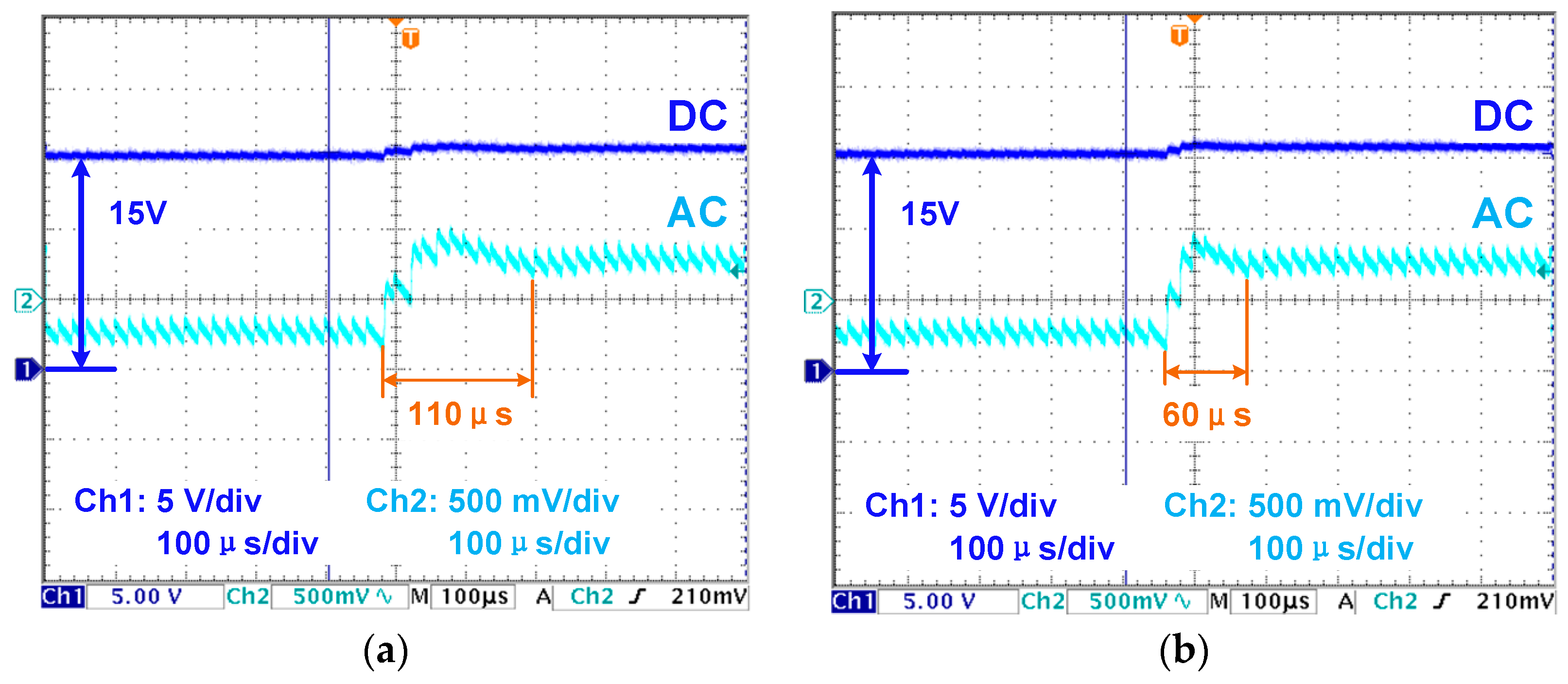
When vref steps from 15 V To 15.5 V, transient responses of output voltage are given in Figure 18. For a converter with a basic SCB controller, the output voltage tracks vref in 110 μs. With the OSCB controller, the output voltage tracks vref in 60 μs. Therefore, the proposed OSCB controller improves the transient response speed by 45% when the reference voltage steps.
As experimental results show, the proposed OSCB controller improves the accuracy of current observation and transient response of the output voltage. Compared with the basic SCB control strategy, which was originally proposed in [21], the OSCB controller decreases the relative error of current observation by 47.1%. Furthermore, the output voltage response time in different transients is shortened by almost half.
6. Conclusions
This paper proposes a damped current model and OSCB controller for flyback converter operating in DCM. The damped current model calculates the output current average value with consideration of parasitics, leakage inductance of the transformer, and the RCD snubber circuit. Based on the model, current observation and control algorithms of SCB controller are optimized, which derives the OSCB controller. Furthermore, a discrete-time small signal model of the converter is given with consideration of current damping. Analyses of the small signal model indicate that the OSCB controller achieves higher closed-loop bandwidth than the SCB controller. Finally, both the accuracy of current observation and transient response of the output voltage are improved, which was verified by experimental results.
Author Contributions
Methodology, R.M.; Supervision, D.Z.; Validation, X.Z.; Writing—original draft, X.Z.; Writing—review & editing, Y.W.
Funding
This work was supported by the National Natural Science Foundation of China under Grant 61701184.
Acknowledgments
This work is supported by Harbin Institute of Technology Shenzhen Graduate School and Huazhong University of Science and Technology.
Conflicts of Interest
The authors declare no conflict of interest.
References
- Cheng, C.H.; Chen, C.J.; Wang, S.S. Small-Signal Model of Flyback Converter in Continuous-Conduction Mode with Peak-Current Control at Variable Switching Frequency. IEEE Trans. Power Electron. 2018, 33, 4145–4156. [Google Scholar] [CrossRef]
- Tavassol, M.M.; Farzanehfard, H.; Adib, E. Single-stage soft-switched PWM flyback power factor correction with reduced dead angle. IET Power Electron. 2017, 10, 1422–1429. [Google Scholar] [CrossRef]
- Wang, Y.; Zhang, S.; Guan, Y.; Liu, X.; Xu, D. Single-stage QR AC-DC converter based on buck-boost and flyback circuits. IET Power Electron. 2017, 10, 103–111. [Google Scholar] [CrossRef]
- Edwin, F.F.; Xiao, W.; Khadkikar, V. Dynamic Modeling and Control of Interleaved Flyback Module-Integrated Converter for PV Power Applications. IEEE Trans. Ind. Electron. 2014, 61, 1377–1388. [Google Scholar] [CrossRef]
- Lee, S.H.; Cha, W.J.; Kwon, B.H.; Kim, M. Discrete-Time Repetitive Control of Flyback CCM Inverter for PV Power Applications. IEEE Trans. Ind. Electron. 2016, 63, 976–984. [Google Scholar] [CrossRef]
- Tamyurek, B.; Torrey, D.A. A Three-Phase Unity Power Factor Single-Stage AC-DC Converter Based on an Interleaved Flyback Topology. IEEE Trans. Power Electron. 2011, 26, 308–318. [Google Scholar] [CrossRef]
- Kim, H.; Lee, J.S.; Lai, J.S.; Kim, M. Iterative Learning Controller with Multiple Phase-Lead Compensation for Dual-Mode Flyback Inverter. IEEE Trans. Power Electron. 2017, 32, 6468–6480. [Google Scholar] [CrossRef]
- Christidis, G.C.; Nanakos, A.C.; Tatakis, E.C. Hybrid Discontinuous/Boundary Conduction Mode of Flyback Microinverter for AC-PV Modules. IEEE Trans. Power Electron. 2016, 31, 4195–4205. [Google Scholar] [CrossRef]
- Ji, Y.H.; Jung, D.Y.; Kim, J.H.; Lee, T.W.; Won, C.Y. A current shaping method for PV-AC module DCM-flyback inverter under CCM operation. In Proceedings of the 8th International Conference on Power Electronics—ECCE Asia, Jeju, Korea, 30 May–3 June 2011; pp. 2598–2605. [Google Scholar]
- Zumel, P.; Garcia, O.; Oliver, J.A.; Cobos, J.A. Differential-Mode EMI Reduction in a Multiphase DCM Flyback Converter. IEEE Trans. Power Electron. 2009, 24, 2013–2020. [Google Scholar] [CrossRef] [Green Version]
- Pagliosa, M.A.; Faust, R.G.; Lazzarin, T.B.; Barbi, I. Input-series and output-series connected modular single-switch flyback converter operating in the discontinuous conduction mode. IET Power Electron. 2016, 9, 1962–1970. [Google Scholar] [CrossRef]
- Johny, L.M.K.; Sebastian, T.K.J. A flyback DCM DC-AC converter for PV applications. In Proceedings of the 2013 Annual International Conference on Emerging Research Areas and 2013 International Conference on Microelectronics, Communications and Renewable Energy, Kanjirapally, India, 4–6 June 2013; pp. 1–6. [Google Scholar]
- Li, H.Y.; Chen, H.C. Dynamic Modeling and Controller Design for a Single-Stage Single-Switch Parallel Boost-Flyback-Flyback Converter. IEEE Trans. Power Electron. 2012, 27, 816–827. [Google Scholar] [CrossRef]
- Chu, G.M.L.; Lu, D.D.C.; Agelidis, V.G. Practical application of valley current mode control in a flyback converter with a large duty cycle. IET Power Electron. 2012, 5, 552–560. [Google Scholar] [CrossRef]
- Hou, Z.Y.; Huang, T.W.; Wang, C.C. On-chip accurate primary-side output current estimator for flyback LED driver control. In Proceedings of the 2016 International Conference on IC Design and Technology (ICICDT), Ho Chi Minh, Vietnam, 27–29 June 2016; pp. 1–4. [Google Scholar]
- Zhang, Y.; Hendrix, M.A.M.; Duarte, J.L.; Lomonova, E.A. Flyback converter using an observer-based digital controller. In Proceedings of the 2015 17th European Conference on Power Electronics and Applications (EPE’15 ECCE-Europe), Geneva, Switzerland, 8–10 September 2015; pp. 1–10. [Google Scholar]
- Shi, L.F.; Qi, Y.M. Current estimation circuit for discontinuous conduction mode flyback pulse-width modulation controller. IET Power Electron. 2015, 8, 1217–1223. [Google Scholar] [CrossRef]
- Lee, J.H.; Lee, J.S.; Lee, K.B. Current sensorless MPPT method for a PV flyback microinverters using a dual-mode. In Proceedings of the 2014 International Power Electronics Conference (IPEC-Hiroshima 2014—ECCE ASIA), Hiroshima, Japan, 18–21 May 2014; pp. 532–537. [Google Scholar]
- Xie, X.; Wang, J.; Zhao, C.; Lu, Q.; Liu, S. A Novel Output Current Estimation and Regulation Circuit for Primary Side Controlled High Power Factor Single-Stage Flyback LED Driver. IEEE Trans. Power Electron. 2012, 27, 4602–4612. [Google Scholar] [CrossRef]
- Min, R.; Tong, Q.; Zhang, Q.; Zou, X.; Yu, K.; Liu, Z. Digital Sensorless Current Mode Control Based on Charge Balance Principle and Dual Current Error Compensation for DC-DC Converters in DCM. IEEE Trans. Ind. Electron. 2016, 63, 155–166. [Google Scholar] [CrossRef]
- Qiu, Y.; Chen, X.; Liu, H. Digital Average Current-Mode Control Using Current Estimation and Capacitor Charge Balance Principle for DC-DC Converters Operating in DCM. IEEE Trans. Power Electron. 2010, 25, 1537–1545. [Google Scholar]
- Akbarabadi, S.A.; Atighechi, H.; Jatskevich, J. Circuit-averaged and state-space-averaged-value modeling of second-order flyback converter in CCM and DCM including conduction losses. In Proceedings of the 4th International Conference on Power Engineering, Energy and Electrical Drives, Istanbul, Turkey, 13–17 May 2013; pp. 995–1000. [Google Scholar]
- Suntio, T. Average and small-signal modeling of self-oscillating flyback converter with applied switching delay. IEEE Trans. Power Electron. 2006, 21, 479–486. [Google Scholar] [CrossRef]
- Luchetta, A.; Manetti, S.; Piccirilli, M.C.; Reatti, A.; Kazimierczuk, M.K. Derivation of network functions for PWM DC-DC Buck converter in DCM including effects of parasitic components on diode duty-cycle. In Proceedings of the 2015 IEEE 15th International Conference on Environment and Electrical Engineering (EEEIC), Rome, Italy, 10–13 June 2015. [Google Scholar]
- Luchetta, A.; Manetti, S.; Piccirilli, M.C.; Reatti, A.; Kazimierczuk, M.K. Effects of parasitic components on diode duty cycle and small-signal model of PWM DC-DC buck converter in DCM. In Proceedings of the 2015 IEEE 15th International Conference on Environment and Electrical Engineering (EEEIC), Rome, Italy, 10–13 June 2015. [Google Scholar]
Figure 1.
Flyback converter with sensorless charge balance controller.

Figure 2.
Output voltage and current under charge balance principle.

Figure 3.
Flyback converter. (a) circuit scheme, (b) currents when operating in DCM.

Figure 4.
Ideal discrete-time small signal model of SCB controlled flyback converter.

Figure 5.
Flyback converter with optimized sensorless charge balance controller.

Figure 6.
Flyback converter with consideration of parasitics, leakage inductance of transformer and RCD snubber circuit. (a) Circuit scheme, (b) Currents of primary and secondary windings.
Figure 6.
Flyback converter with consideration of parasitics, leakage inductance of transformer and RCD snubber circuit. (a) Circuit scheme, (b) Currents of primary and secondary windings.

Figure 7.
Flyback converter in switch-on state. (a) Active circuit, (b) Equivalent circuit scheme.

Figure 8.
Flyback converter in transform state. (a) Active circuit, (b) Equivalent circuit scheme.

Figure 9.
Flyback converter in switch-off state. (a) Active circuit, (b) Equivalent circuit scheme.

Figure 10.
The observed current values based on different observers. (a) ACO, (b) DACO.

Figure 11.
Duty cycle calculated by different current controllers. (a) ACC, (b) DACC.

Figure 12.
Discrete-time small signal models with consideration of current damping. (a) SCB control, (b) OSCB control.
Figure 12.
Discrete-time small signal models with consideration of current damping. (a) SCB control, (b) OSCB control.

Figure 13.
Frequency responses of the closed-loop systems.

Figure 14.
Photograph of the experimental prototype.

Figure 15.
Comparison among the measured output current average value, the observed current from ACO and the observed current from DACO.
Figure 15.
Comparison among the measured output current average value, the observed current from ACO and the observed current from DACO.

Figure 16.
Output voltages when vg steps from 10 V to 7.5 V. (a) SCB controller, (b) OSCB controller.
Figure 16.
Output voltages when vg steps from 10 V to 7.5 V. (a) SCB controller, (b) OSCB controller.

Figure 17.
Output voltages when R steps from 50 Ω to25 Ω. (a) SCB controller, (b) OSCB controller.

Figure 18.
Output voltages when vref steps from 15 V to 15.5 V. (a) SCB controller, (b) OSCB controller.
Figure 18.
Output voltages when vref steps from 15 V to 15.5 V. (a) SCB controller, (b) OSCB controller.


Table 1.
Specifications of the Tested Flyback Converter.
| Lm | C | vg | v | T | N |
|---|---|---|---|---|---|
| 15 V |
© 2018 by the authors. Licensee MDPI, Basel, Switzerland. This article is an open access article distributed under the terms and conditions of the Creative Commons Attribution (CC BY) license (http://creativecommons.org/licenses/by/4.0/).
Share and Cite
MDPI and ACS Style
Zhang, X.; Min, R.; Zhang, D.; Wang, Y. An Optimized Sensorless Charge Balance Controller Based on a Damped Current Model for Flyback Converter Operating in DCM. Energies 2018, 11, 3478. https://doi.org/10.3390/en11123478
AMA Style
Zhang X, Min R, Zhang D, Wang Y. An Optimized Sensorless Charge Balance Controller Based on a Damped Current Model for Flyback Converter Operating in DCM. Energies. 2018; 11(12):3478. https://doi.org/10.3390/en11123478
Chicago/Turabian StyleZhang, Xiaofeng, Run Min, Donglai Zhang, and Yi Wang. 2018. "An Optimized Sensorless Charge Balance Controller Based on a Damped Current Model for Flyback Converter Operating in DCM" Energies 11, no. 12: 3478. https://doi.org/10.3390/en11123478
Note that from the first issue of 2016, this journal uses article numbers instead of page numbers. See further details here.