Suppression of Switching Crosstalk and Voltage Oscillations in a SiC MOSFET Based Half-Bridge Converter


School of Automation, Northwestern Polytechnical University, Xi’an 710000, China
*
Authors to whom correspondence should be addressed.
Energies 2018, 11(11), 3111; https://doi.org/10.3390/en11113111
Submission received: 13 October 2018
/
Revised: 7 November 2018
/
Accepted: 9 November 2018
/
Published: 10 November 2018
(This article belongs to the Special Issue Power Electronics 2018)
Abstract
:The silicon carbide (SiC) MOSFET is characterized by high operating voltage, temperature, switching frequency and efficiency which enables a converter to achieve high power density. However, at high switching frequency, the crosstalk phenomenon occurs when the gate voltage spike introduced by high dv/dt and voltage ringing forces false turn-on of SiC MOSFET which causes a crow-bar current thereby increasing switching losses. In order to increase the immunity against the crosstalk phenomenon in a half-bridge configuration, this paper presents a gate driver for SiC MOSFET capable of generating the negative turn-off voltage without using a negative power supply. In addition, the effect of parasitic inductances on the switching response is analyzed and an RC snubber is designed using high-frequency based circuit reduction technique to dampen the switching ringing. The performance of the proposed gate driver and the designed RC snubber is validated using simulation and experiment at the 1 MHz switching frequency. The results show that the proposed gate driver with RC snubber eliminates crosstalk by maintaining any spurious gate spike below the gate threshold voltage.
1. Introduction
The demand for fast-switching, high voltage, and high-temperature devices, capable of operating at elevated efficiency has enabled the trend towards WBG semiconductor materials [1,2]. Among the WBG, the SiC and GaN technologies have matured enough and devices up to 1.7 kV and 650 V voltage ratings respectively, are commercially available which have been proved as promising alternatives to the Si. Due to an almost identical gate drive requirements, the GaN cascode transistor can easily replace Si MOSFET [3]. However, due to features such as a restricted-range of gate voltage, low threshold voltage, and low parasitic capacitances the gate drive requirements of a SiC MOSFET are more stringent [4,5].
The recent research focuses on the gate driver design for SiC MOSFET to enable the high switching speed, also featuring the damping of parasitic resonance and crosstalk suppression [6,7]. The crosstalk phenomena in half-bridge configuration refer to the spurious triggering of the low-side SiC MOSFET during the turn-on transition of the high-side SiC MOSFET and vice versa [8]. Due to voltage rise across the device in off-state, a charging current flow through its parasitic gate-drain capacitance and induces a positive spike in its gate voltage. When this voltage spike exceeds the gate threshold voltage, it can falsely trigger the high-side MOSFET, which causes a crow-bar current and result in increased switching power losses. Therefore, it is essential to suppress the crosstalk phenomena for the high-frequency and reliable operation of the half-bridge converter [9].
The gate-impedance control technique reduces the gate voltage spike by adding external gate-source capacitance to provide a low-impedance path [10,11]. However, the crosstalk mitigation is vestigial as it results in a prolonged switching transition, increasing the switching losses [12]. The active suppression technique reported in [13], employed a transistor between the gate and source terminals to create a short when the gate-source voltage climb above the threshold voltage is detected. However, due to the high internal gate and source impedances, the gate voltage feedback for crosstalk detection lacks accuracy and degrades the effectiveness of active suppression system.
Another reported technique used a negatively biased gate voltage, which by level shifting the gate voltage spike prevents false turn-on and accelerates the SiC MOSFET’s turn-off [14]. The negative turn-off voltage is commonly supplied using an additional negative voltage source, but, the level shifter circuits proposed in [15,16] used voltage divider circuit to get rid of the negative voltage source. However, due to increased circuit complexity, it is not a viable solution for volume optimized and cost-sensitive converters. In this paper, a gate driver is proposed for SiC MOSFET to suppress the crosstalk phenomena by a negative level shifting of the gate voltage using a parallel connected zener diode and a capacitor. Furthermore, the proposed driver circuit does not require a dedicated negative voltage source and voltage feedback and is realized using low-cost components.
The parasitic inductance and stray capacitance of SiC MOSFET at a high-switching frequency manifest resonance which introduces a voltage overshoot and ringing during turn-off transition [17]. The parasitic package inductances of the SiC MOSFET becomes further unpropitious when combined with the stray inductance of PCB interconnection [18]. The parasitic inductance reinforces voltage overshoot which deteriorates the total harmonic distortion (THD) performance, and as a result, the converter may require a higher-order filter to meet the desired performance. Therefore, it is necessary to suppress the parasitic resonance to enable improved THD of half-bridge dc-ac converter or otherwise; the high-frequency operation will be vestigial [19].
Optimization of package inductances for pushing higher the parasitic resonant frequency is becoming faltered, and therefore, the conspicuous solution is to maneuver the impedance of the switching circuit using an auxiliary network [20]. Several techniques aimed to suppress the voltage ringing, range in complexity from reducing the switching speed using high gate impedance to active gate control involving a feedback compensator [21,22]. The simplest approach advocates lowering the switching speed by raising the gate impedance, however, the prolonged switching transition enlarges switching losses [23]. Due to magnetic saturation caused by current escalation limits application of ferrite bead to restrain the parasitic inductance. Moreover, the suppression using dc-link capacitors [24] and magnetically coupled damping circuits [25] is not very convincing. The RC shunt snubber is the familiar and most effective technique which offers flexibility to achieve the desired level of suppression. However, the experience-based design commonly leads to inadequate damping [26]. In [27], the authors formulated a root-locus based RC snubber design for the double-pulse circuit by neglecting the parasitic source inductance of the SiC MOSFET. In this work, the same design procedure is adapted to optimize the suppression circuit for the half-bridge dc-ac converter while the SiC MOSFET embodies the parasitic source inductance.
The rest of this paper is organized as follows. The gate driver for SiC MOSFET is presented in Section 2. Effect of parasitic components on switching response is illustrated in Section 3. In Section 4, the snubber circuit design is proposed for mitigating the switching ringing. Simulation and experimental results are presented in Section 5, followed by the conclusion in Section 6.
2. Gate Driver for SiC MOSFET
2.1. Crosstalk Phenomenon in Half-Bridge dc-ac Converter
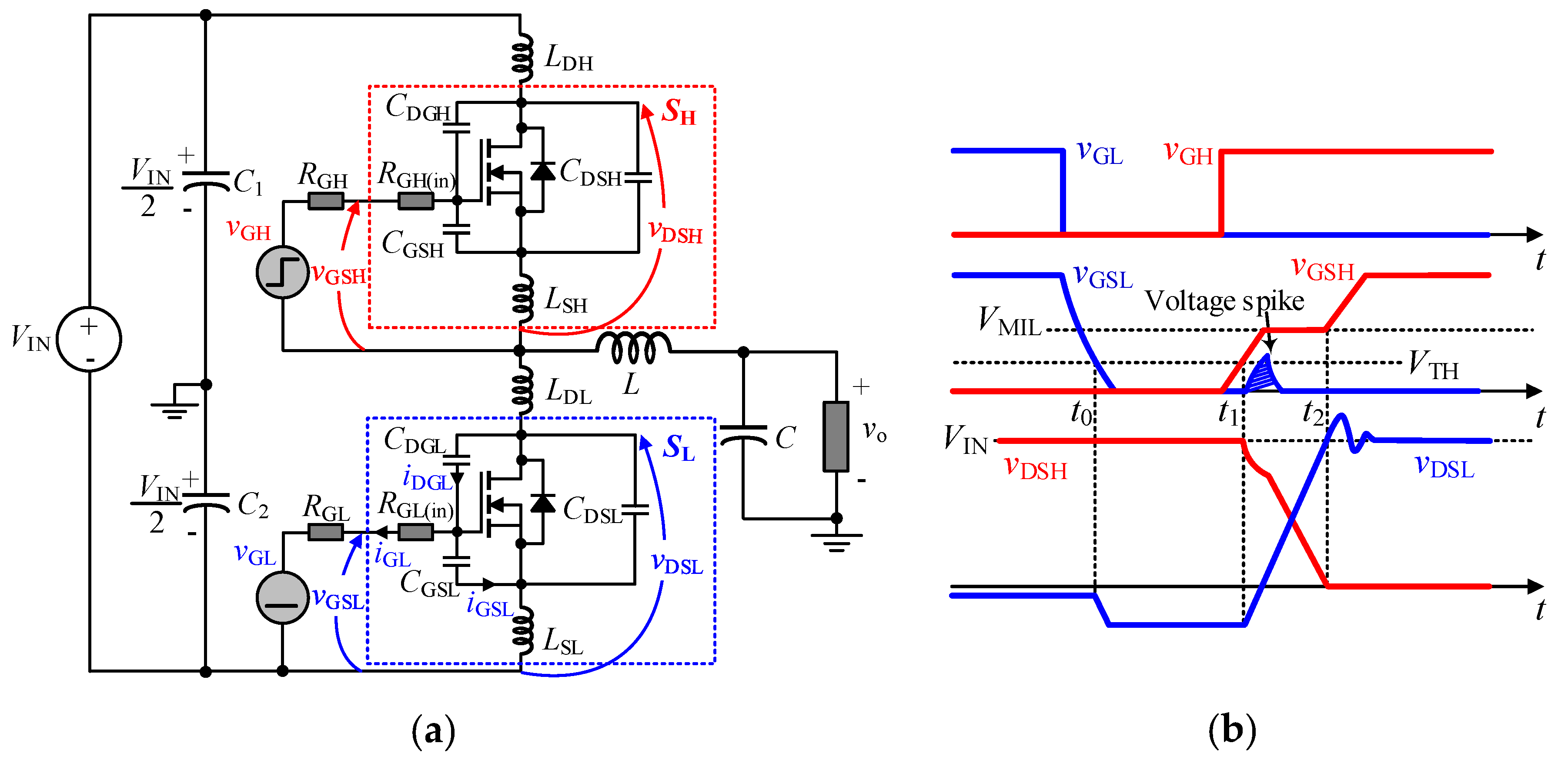
Due to fast-rising drain-source voltage, the parasitic capacitances of a MOSFET cause a gate voltage spike during switching transitions and may result in spurious turn-on if it exceeds the threshold voltage. The SiC MOSFET is more vulnerable to false triggering due to its low-threshold voltage as compared to Si counterpart. For instance, the typical threshold voltage of Si MOSFET IPW65R190CFD from Infineon Technologies is 4 V, while for SiC MOSFET C3M0120090J from Cree Inc., the value is only 2.1 V. A detailed schematic of the half-bridge dc-ac converter, including the parasitic components of SiC MOSFET is shown in Figure 1a. The driving voltages vGH and vGL control the switching state of the high-side SH and low-side SL MOSFETs respectively. Further, the RGL and RGL(in) are the external and internal gate resistances of low-side MOSFET SL respectively, while CGSL, CDGL, and CDSL are its parasitic gate-source, drain-gate, and drain-source capacitances respectively.
It is assumed that SL is in its blocking state, and the MOSFET SH is tuning-on as shown in Figure 1b to illustrate the mechanism of spurious gate voltage spike. At time t1, the vGSH crosses the threshold voltage VTH, which allows the drain-source voltage of the low-side MOSFET vDSL to rise abruptly, producing a current iDGL through parasitic capacitance CDGL. This charging current iDGL further flows through the parasitic capacitance CGSL and the gate resistors RGL(in) and RGL, respectively denoted as iGSL and iGL. The current iGL introduces a spike in the gate voltage vGSL with the peak determined by RGL, CGSL, and CDGL. Consequently, a spurious turn-on of the low-side MOSFET occurs if the resulting voltage spike exceeds the threshold voltage VTH. A likely method to reduce iGL is by adding external gate-source capacitance, which not only shunts the iDGL but also useful in suppressing the resonance due to the stray inductance and gate-source capacitance CGSL. However, the external gate-source capacitance increases the rise time of the gate voltage and thereby results in increased switching losses. In this paper, the crosstalk suppression by level-shifting of the gate voltage is adopted using a gate driver that does not require a dedicated negative voltage source and voltage feedback while is realized only using passive components.
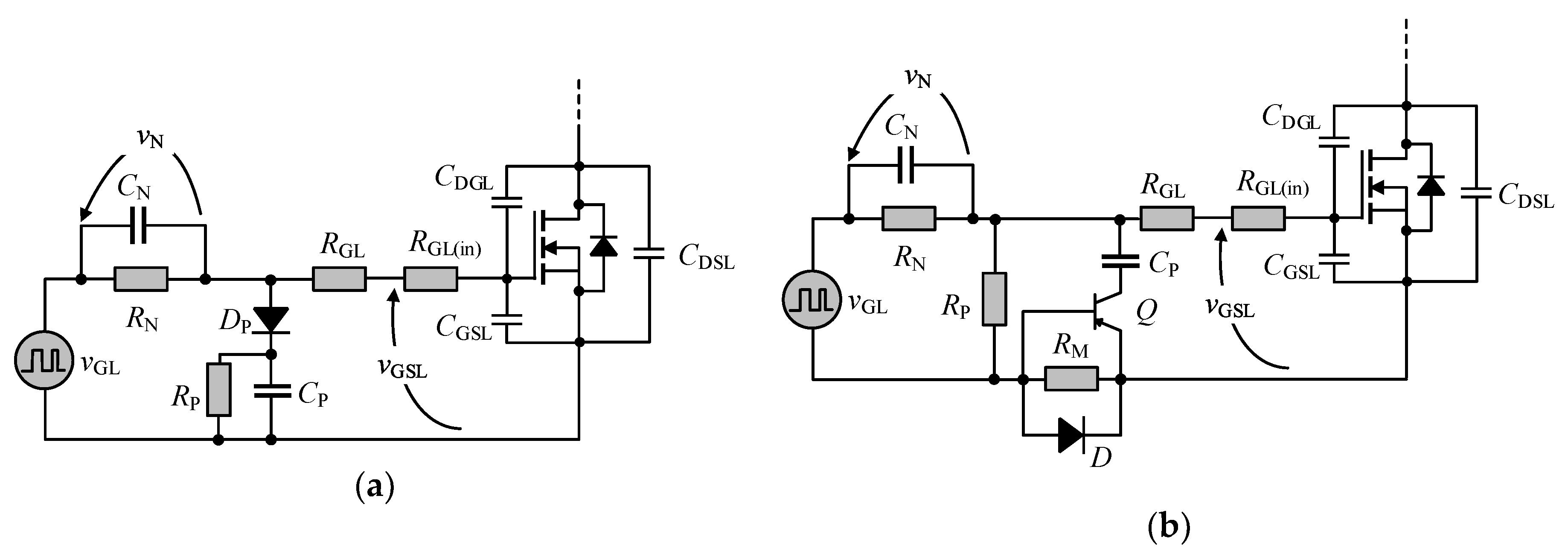
2.2. Previous Work on Gate Driver for SiC MOSFET with Level Shifter
To increase the immunity of SiC MOSFET against the crosstalk phenomenon in a half-bridge configuration, a gate driver capable of generating the negative turn-off voltage without using a negative power supply is trending. The reason is that the elimination of negative voltage supply significantly reduces the complexity in the converter’s layout design. However, it is required that the level shifter circuit must be simple and effective to justify the replacement. Two of the recently reported gate drivers use RCD level shifter and voltage divider circuit.
The RCD level shifter [15] consists of two pairs of parallel connected resistor and capacitor and a diode as shown in Figure 2a. The diode DP conducts when the driving voltage vGL is high, otherwise it operates in the blocking mode. For CP and CN >> CGSL, conduction of DP sets the steady-state vN as given by Equation (1). When vGL flips back to the low-state, the DP disconnects the RP-CP and forcing the turn-off gate current to flow through RN-CN branch. Therefore, the applied gate voltage is level shifted by VN.
A modified version of the RCD level shifter reported in [28] is shown in Figure 2b, in which the offset in the gate voltage is also given by Equation (1). During turn-on of SiC MOSFET, the gate current returns through resistor RM which triggers the transistor Q by creating a positive emitter-base voltage. The capacitor CP precharged by gate driving voltage, charges CGSL to avoid delays in turning-on. During turn-off of SiC MOSFET, the current flows through diode D when the capacitor CN acts as local voltage source to supply negative voltage.
2.3. Proposed Gate Driver for SiC MOSFET
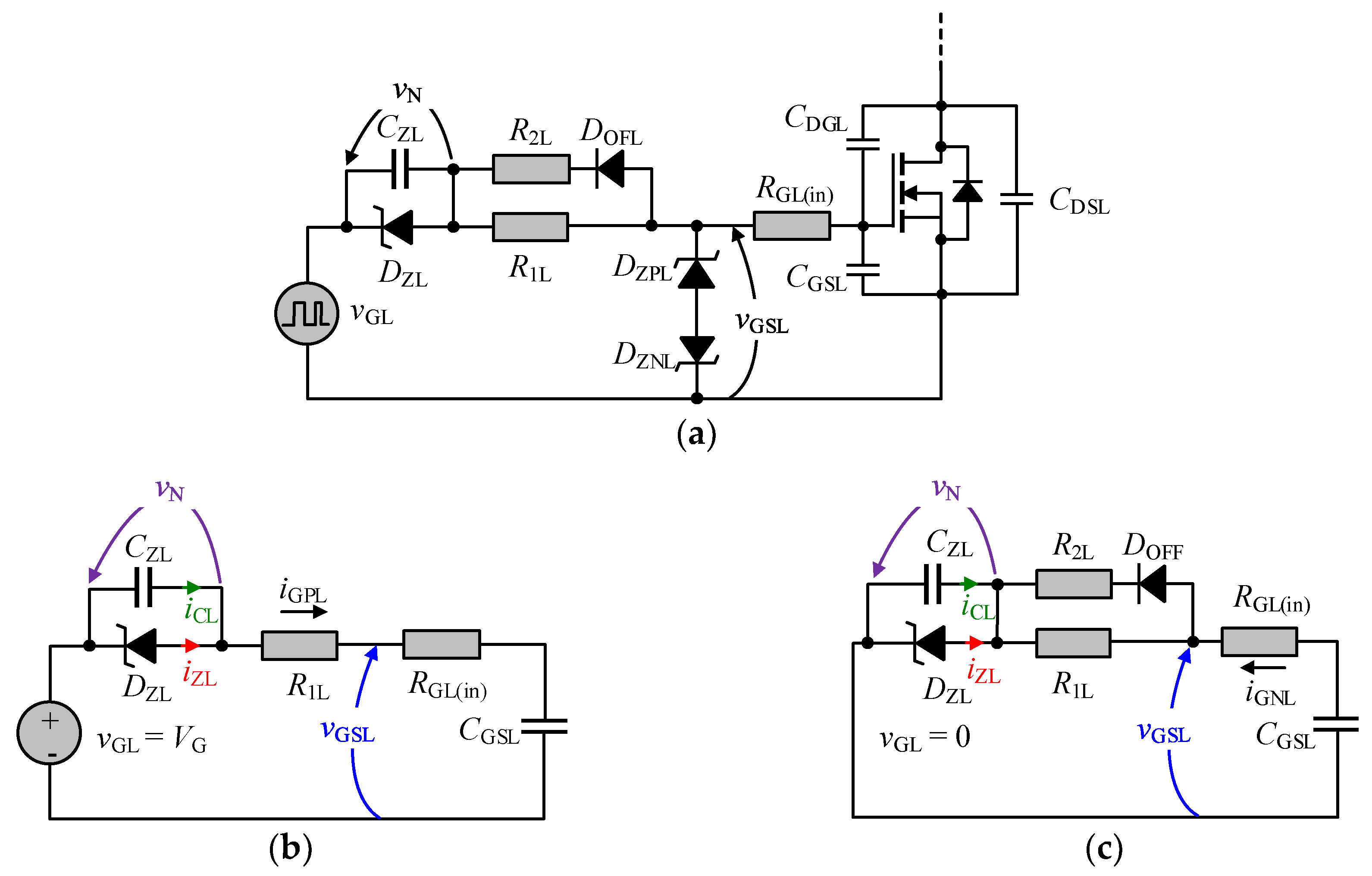
The proposed gate driver is shown in Figure 3a only for low-side MOSFET, which is comprised of a capacitor CZL, an ultra-fast diode DOFL, two resistors R1L and R2L, and three zener diodes DZL, DZPL and DZNL. The components of the high-side driver use similar notation, except their subscripts end with the letter “H” instead of letter “L”. The parallel connected zener diode DZL and capacitor CZL generates a negative gate voltage and thus perform the voltage level shifting without using a negative voltage supply. Due to narrow operating gate voltage range, i.e., 8/18 V, two zener diodes are used as a voltage clipper between the gate and source terminals to protect the MOSFET against the gate breakdown. The diode DOFL enables a lower impedance path for the turn-off gate current to accelerate the turn-off transition. When the diode DOFL is forward biased, a lower turn-off gate resistance is realized by the parallel connection of resistors R1L and R2L.
The design criterion of the components is approached through the transient analysis of the proposed gate driver. Mathematical expressions are derived for gate-source voltage during turn-on and turn-off process.
2.3.1. Turn-on Process
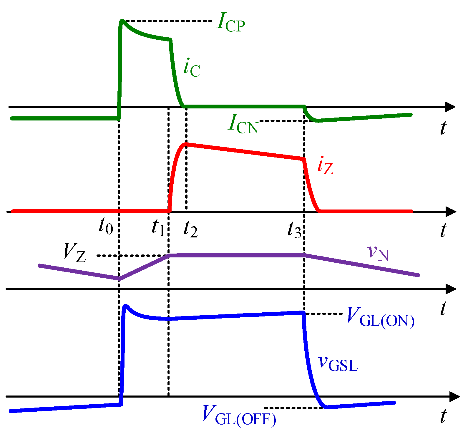
An equivalent circuit of the gate driver when the gate drive voltage vGL steps from 0 to VG at time t0 is shown in Figure 3b. The inceptive gate current iGPL path comprises the components CZL, R1L, RGL(in) and CGSL, ramping up the voltage vN to the zener voltage VZ of the diode DZL. As a result, the current through the zener diode denoted as iZL rises and take over the capacitor current iCL regulating vN at VZ. This indicates that iGPL is the algebraic sum of the capacitor current iCL and the current through the zener diode iZL. Kirchhoff voltage law (KVL) is applied to the equivalent circuit in Figure 3b which gives Equation (1) which is essential to derive the mathematical relation for iGPL.
Using the Laplace transform, the solution of the integral equations in (2) are given in (3)
where t1 is the time required to charge CZL to voltage VZ, and τa and τb are the time constants expressed in (4). Equation (3) indicates that the peak iGPL is determined by the driving voltage VG, and the external and intrinsic gate resistors, i.e., R1L and RGL(in). Since τa > τb, the current iZL decays faster than iCL. However, for the desired level shifting operation, the zener diode must not cease conduction until the vGL step to 0 V.
It is essential to observe vGSL as gate-source voltage determines the MOSFET turn-on. Using KVL the voltage equation is given as
substituting iGPL gives the vGSL expressed in (6). It indicates that the decay rate of vGSL can be controlled by tuning CZL and R1L. To prevent the abrupt drop of vGSL the criteria, i.e., CZL >> CGSL, should be ensured.
2.3.2. Turn-off Process
When vGL steps to 0 V, the diode DOFL provides a low impedance path for the gate drive current iGNL, turning-off MOSFET as shown in Figure 3c. It is desirable to use low-valued external gate resistance as it shortens the turn-off time. The Kirchhoff voltage law applied to the equivalent circuit in Figure 3c gives the integral equation
where RTL = R1L//R2L. Again, solving the Equation (7) using the Laplace Transform gives the gate loop current iGPL and voltage-source vGSL voltage as
where τc is the time constant of the equivalent driver circuit during turn-off and is expressed by
The capacitor CZL, precharged up to voltage VZ serves as a local storage and supplies a negative gate voltage during turn-off without using a dedicated negative voltage supply. Again, to maintain the negative gate voltage, the value of CZL must satisfy the condition
where Dm is the expected maximum duty-cycle, and TS is the switching period.
Equations (6) and (8) indicate that the proposed gate driver level shift vGSL by −VZ and thus toggles between −VZ and VG − VZ voltage levels. The negative bias voltage has a negligible effect on the turn-on transient of the MOSFET, but accelerates the turn-off as illustrated by the waveforms of the proposed gate driver in Figure 4.
3. Effect of Parasitic Inductances on Switching Waveform of SiC MOSFET
The demand for miniaturized power converters pushes the semiconductor devices to operate at higher switching frequencies. However, the parasitic inductances from PCB interconnections and device packages together with the stray capacitances of the SiC MOSFET can influence switching operation due to high di/dt [29,30]. They causes parasitic resonances which increase electrical stress [31] and slow down the rise and fall of drain current [32]. Therefore, it is important to model effect of parasitic components on switching characteristics. For the study, a conduction overlap is assumed, followed by the low-side MOSFET turn-off transient.
3.1. Overlap Conduction
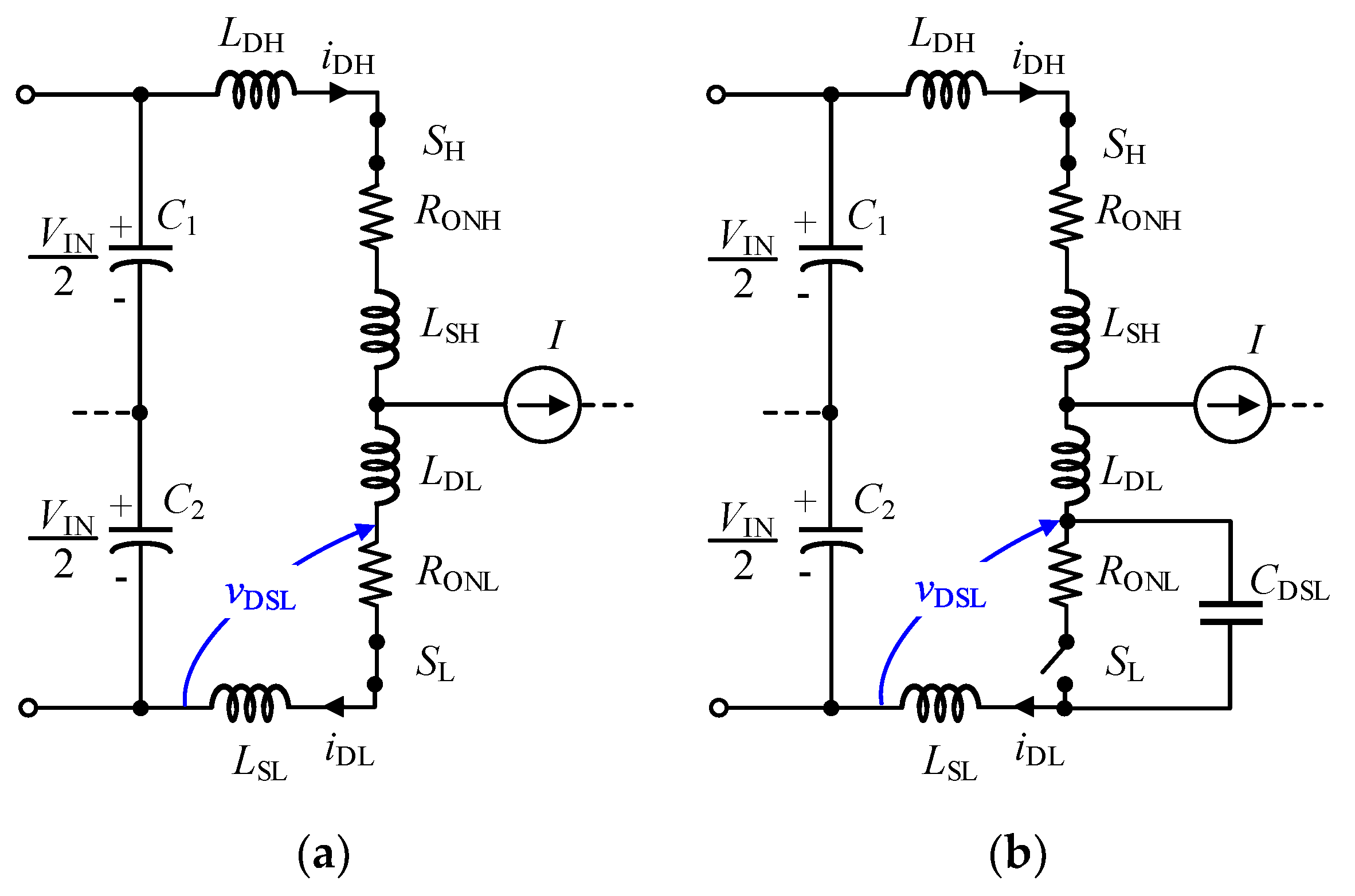
In the presence of interconnection inductances, an overlap in the conduction of two switches is first investigated to recognize the effect on the turn-off process. Figure 5a shows the half-bridge dc-ac converter with lumped package and interconnection inductances. The LDH and LDL represent the drain inductances, and LSH and LSL represent source inductances of SH and SL MOSFETs respectively. When the dead-time is too short, there is overlap conduction which allows a momentary crow-bar current. It is assumed that switch SL is initially conducting current Io and before its transition to blocking state, the high-side MOSFET SH turns-on creating a crow-bar current. Therefore, MOSFETs SH and SL are replaced with close switches with conduction resistance RONH and RONL respectively. The inductor current is assumed as a current source I in order to simplify the analysis. The voltage equations of the equivalent circuit during overlap conduction are given as
using iDH = I + iDL in (11), and using Laplace transform to solve, the low-side drain current iDL and drain voltage vDSL are expressed as follows.
Assuming RONL = RONH, Equation (11) indicates that vDSL will approach 0.5 × (VIN − IRONH) during the overlap time of length Toc, energizing the parasitic inductances.
3.2. The SL Turn-off Transient
Following the overlap conduction, the transition of low-side MOSFET from conduction to blocking state is shown in Figure 5b, with SL replaced with an open switch. During this switching transition, the interconnection inductances release their previously stored energy. The drain-source capacitance CDSL and inductances LDL and LSL of the low-side MOSFET realizes a resonant circuit which introduces oscillations in vDSL. The circuit equation during SL turn-off is given as
Differentiation of (14) and using iDH = I + iDL, reduces the circuit equation to the following standard form
where the resonance frequency ωr and damping factor ζ are related to the parasitic components as
Using the Laplace transform, the equation for drain current iDL is expressed in (15)
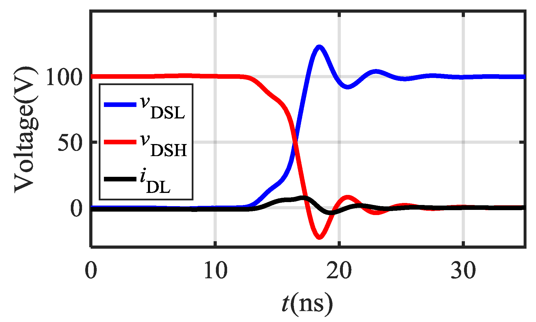
where the initial conditions determine the constants A and B. Due to the equivalent second-order circuit, iDL exhibit underdamped oscillations as determined by the milliohm ranged conduction resistance RONH, forcing vDSL to swing accordingly.
Figure 6 shows the waveform of iDL for overlap conduction interval Toc followed by turn-off of low side MOSFET SL. Assuming an initial 1.2 A steady drain-source current through the body diode of SL, during Toc the cross-bar current forces iDL to rise rapidly. Finally, elapse of Toc results in underdamped oscillations. A significant reduction is noted in the average drain-source voltage which would result in a lower voltage gain of the dc-ac conversion.
3.3. PCB Guidelines
Besides, there is always inescapable intrinsic parasitic inductances of the device, but an adequate PCB layout can optimize the efficiency, enhances the input voltage operating range and reduces the noise among traces of converter [33]. Importantly, minimizing the high-frequency loop inductance enables higher switching frequencies and reduces the voltage overshoot and EMI. Besides improving the THD, it also relaxes the filter requirement. The input path carries the pulsating current and thereby needs special attention as high di/dt and parasitic inductance of a trace can generate voltage ringing [34]. Therefore, it is necessary to minimize the circumference of the high-frequency power-loop.
Conventionally, the power-loop is routed on a single layer known as the lateral power-loop, while the next inner layer is used as a shield plane [19], which reduces the impact of the field generated by high-frequency switching. Due to pulsating current, the power-loop induces a current in the shield layer which produces a magnetic field of its own, counteracting the field of the power-loop. Here the shortest loop has been achieved using the top and the next inner layer (power plane) for laying out the power-loop. Transistors have been placed on the topmost layer, while the internal power plane serves as the return path. Furthermore, the power inductor has been placed on the bottom layer and connected to the drain of MOSFET using vias. Several interleaved channels by assuming vias reduce the current density and thus the interconnection inductances. This results in a smaller power-loop with the field cancellation capability.
The soldering pad for the transistor’s tab serves as the primary heat-sink, and thereby a larger copper area is assigned to spread out the heat. The vias used to connect the power plane, and drain of the high-side MOSFET not only reduces the parasitic inductance but also improves the thermal performance by facilitating heat conduction from top to bottom of the PCB [35]. Since the bottom is a low-resistance path for heat flow, vias on the bottom side are connected to the large copper polygon. Heat sink soldered on the bottom-side is recommended to improve the thermal performance further.
4. RC Snubber for Suppression of Parasitic Ringing
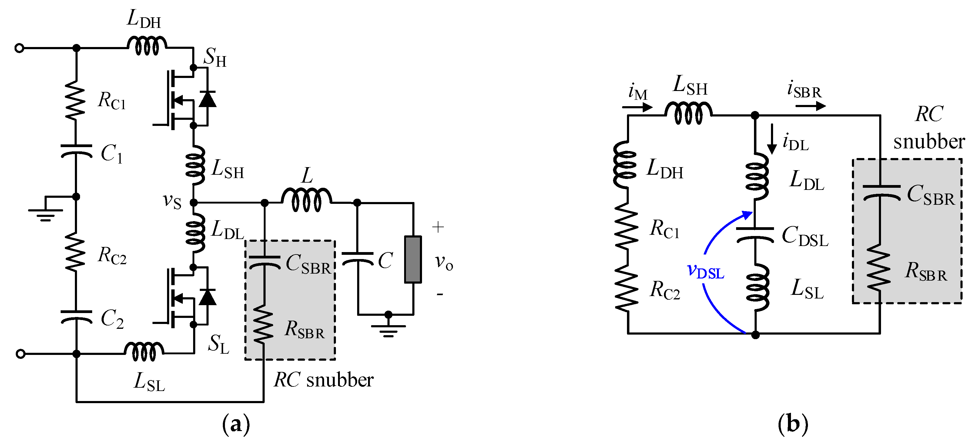
The antecedent section discussed the negative influence of parasitic elements on the switching waveform of SiC MOSFET. The derived equation indicates that due to parasitic inductance and capacitance the drain current undergoes ringing, thereby forcing the drain-source voltage to oscillate [36,37]. Suppression of this obtruded ringing in the switching waveform is vital to ensure low distortion and stunted electromagnetic noise [38]. Here, the objective is to dampen the ringing in the drain-source voltage of the low-side MOSFET SL during turn-off by employing an RC snubber across the SL as shown in Figure 7a. The RSBR and CSBR represent snubber circuit resistance and capacitance respectively, while RC1 and RC2 are the equivalent series resistance (ESR) of dc-link capacitors.
The snubber design starts with deriving an equivalent circuit of Figure 7a using the high-frequency minimization [27]. It is supposed that initially, the low-side MOSFET SL conducts current Io. When the channel resistance increases during the turn-off process, a change in drain-source voltage vDSL causes the drain-source capacitance CDS of the MOSFET to conduct. Finally, neglecting body-diode conduction resistance, replacing large inductances such as L and interconnection inductance between source and converter with open, and replacing dc-link capacitances with short-circuit result in the equivalent circuit shown in Figure 7b. The notation iSBR, iD, and vDSL represent current through snubber, drain current and drain-source voltage of SL respectively. In [27], the authors ignored the parasitic source inductance LSL and assumed vDSL as the voltage across CDS. On the contrary, vDSL is exercised here as the sum of the voltage across CDS and LSL to achieve more accurate analysis.
The next step is to derive the expression for vDSL as a function of initial drain current Io using the equivalent circuit, which gives the rule for snubber components design. Applying KCL and KVL to the equivalent circuit gives the dynamics in (17).
Applying Laplace transform and using ISBR, IDL, IM, and VDSL for the corresponding s-domain functions of iSBR, iDL, iM, and vDSL, respectively, gives Equation (18).
Using (18a)–(18c) in (18d) and solving for VDSL gives (19) in terms of initial drain current Io.
where the numerator N and denominator ∆ are expressed in (19) and (20) respectively.
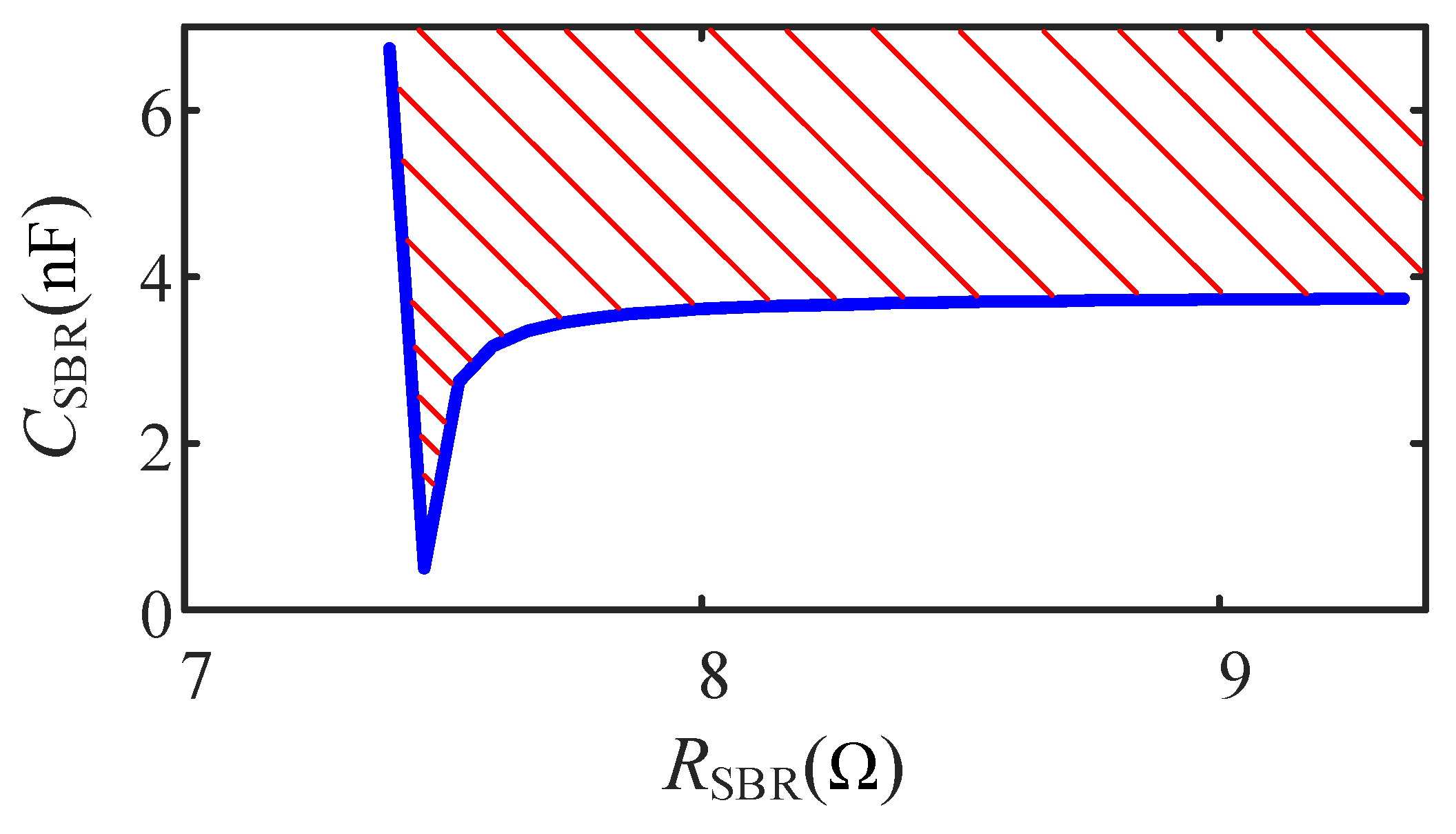
The response of vDSL can be analyzed from the denominator ∆ which give the rules to suppress the ringing. By choosing RSBR and CSBR such that all the roots of ∆(s) are real, ensures successful mitigation of oscillations in vDSL. However, it is not a straightforward to comprehend in case of a fourth-order equation as there is a breakaway point due to the intersection of only two root loci with the real axis. Therefore, to reduce ∆(s) to a third-order polynomial equation, the drain-source inductances of high-side MOSFET are assumed negligibly small. Substitution of LSH = LDH = 0 in (21) and solving algebraic equations ∆(s) = 0 and d∆(s)/dt = 0 for RSBR and CSBR gives
where the NC(s), ∆C(s), NR(s) and ∆R(s) are explicity given in (23)
The final step is to draw RSBR verses CSBR parametric curve by sweeping the variable s in (22), which gives the boundary of the region where all the roots of ∆(s) are real. Since the solutions to ∆(s) = 0 are negative for a stable operation, the parameter s is swept on the negative real axis of the complex plane. Figure 8 shows the resulting parametric curve with the snubber components chosen in the shaded region ensures suppression of switching oscillations. In addition to dampen the voltage vibrations, the snubber must also ensure minimum power losses. Therefore, the lower part of the critically damped region is more suitable as the CSBR significantly affects snubber losses as compared to RSBR.
5. Results and Discussion
In this section, the proposed gate driver performance is verified using computer simulation and experimental prototype of SiC half-bridge dc-ac converter. Specifications of the converter under study are given in Table 1. To simulate the Spice model of SiC MOSFET provided by Cree Inc., LTspice software is used with a step size of 1 ns. Parameters of SiC MOSFET, i.e., C3M0120090J related to the gate driving are listed in Table 2. For reduced conduction losses, 16 V turn-on gate-source voltage is recommended. Since the proposed circuit performs level shifting, therefore, a regulated 18.4 V gate driver source is applied to set +16 V and -2.4 V, as the on and off gate driving voltages respectively. Other specifications of the gate driver components based on its transient analysis are given in Table 3.
5.1. Simulation Results
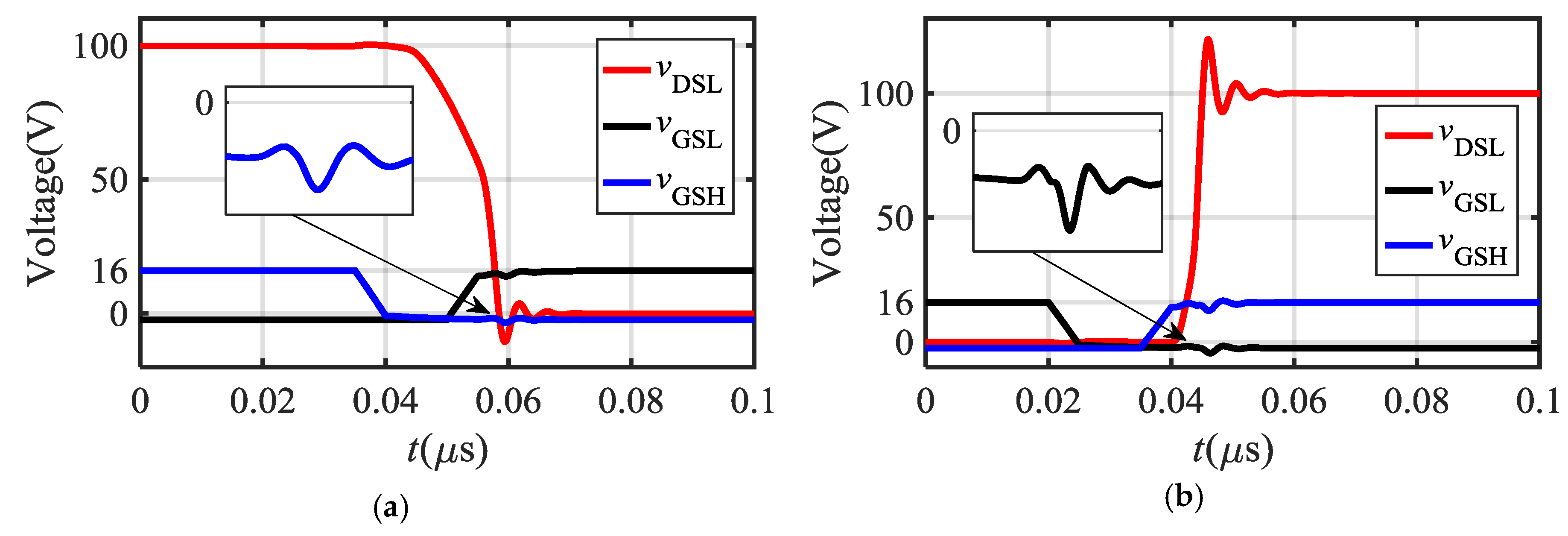
The captured switching waveforms are shown in Figure 9, where the gate-source voltages are level shifted by 2.4 V. During the turn-on process of low-side MOSFET, the vGSL rises to 16V in 5 ns thereby forcing drain-source voltage vDSL to fall as shown in Figure 9a. Below 50 V, the change in vDSL is high, i.e., 15 V/ns, and induces 1.7 V in vGSH. A similar phenomenon is observed in the turning-off waveform shown in Figure 9b. However, due to the level shifted gate-source voltages, there is no spurious turn-on.
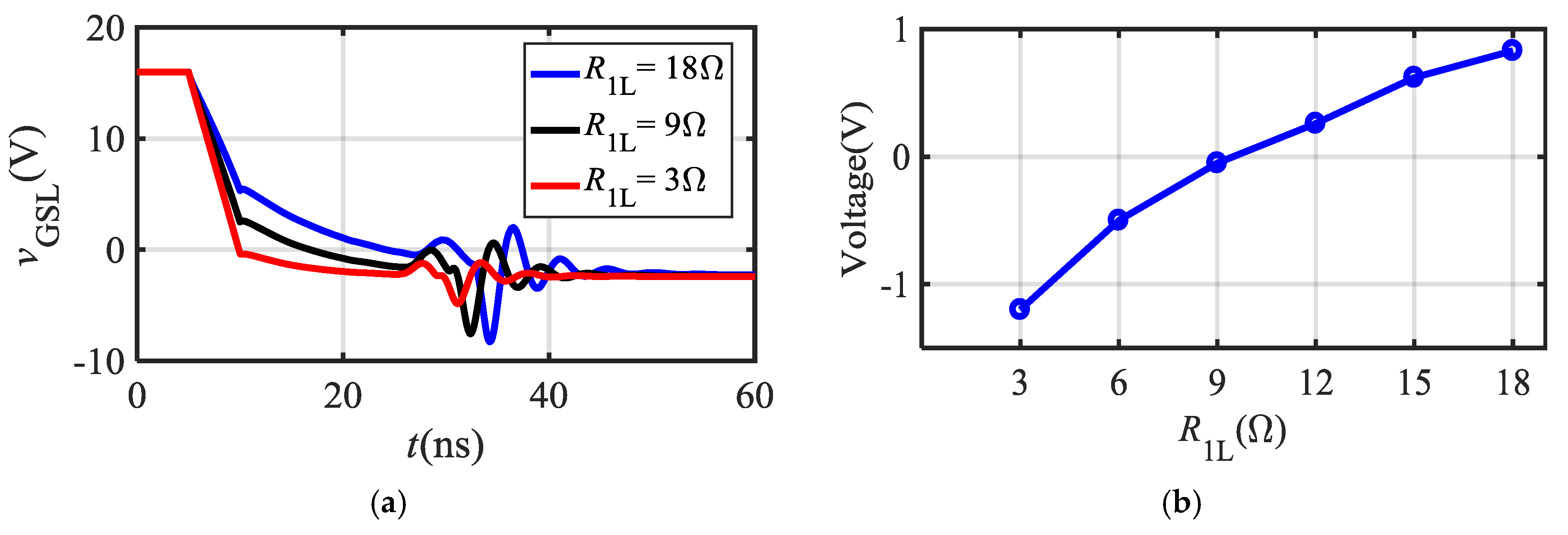
Moreover, using LTspice simulation the effect of gate resistance on the switching operation is investigated. Figure 10a shows the turning-off gate-source waveforms under 3 Ω, 9 Ω, and 18 Ω gate resistances. SiC MOSFET based half-bridge converter is simulated using the Spice model with inductances of 7.46 nH, 1.5 nH, and 7.06 nH added to the source, drain and gate terminals of each MOSFET respectively in order to verify the theoretically analyzed effects of parasitic elements. It is observed that the increase in gate resistance slows down the transition of gate-source voltage and results in higher spurious peaks, which can also be noted from the relationship between gate resistance R1L and gate voltage spike, shown in Figure 10b. Thus, it is significantly important to choose a relatively lower R1L to achieve the desired level shifting and protects the MOSFET from false turn-on. On the other hand, while choosing R2L the high intrinsic gate resistance is particularly noteworthy as spurious turn-on can occur if the voltage drop across R1L//R2L exceeds the gate threshold voltage. Therefore, R2L is chosen same as R1L to ensure the turning-off gate impedance as half of the turning-on counterpart.
Thus, it is concluded that the parasitic inductances negatively influence the switching response of SiC MOSFET, including voltage overshoot exceeding the steady-state drain-source voltage and high-frequency oscillations, thereby enlarging voltage stress and EMI noise. Moreover, since the source inductance couples the power and gate-loop, therefore, the ringing in drain-source voltage forces the gate-source voltage to oscillate accordingly.
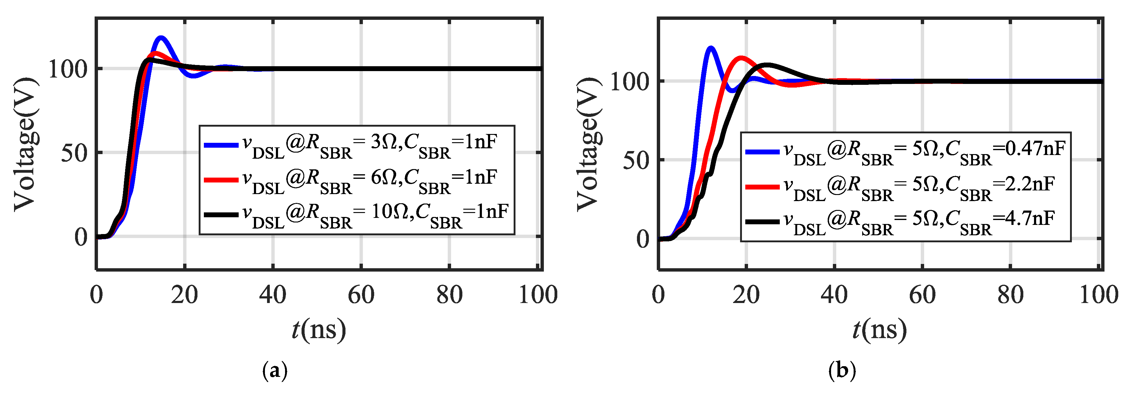
An RC snubber circuit is used to suppress such oscillations. Figure 11 shows the simulation results of voltage ringing using different snubber combinations. Figure 11a shows that raising the RSBR dampens the oscillations, while, the converter simulated for different CSBR and RSBR = 1 Ω is shown in Figure 11b, which indicates that raising CSBR can also suppress the parasitic ringing. However, the power losses significantly increase by raising CSBR [39]. Therefore, its minimum value is chosen for experimental implementation.
5.2. Experimental Results
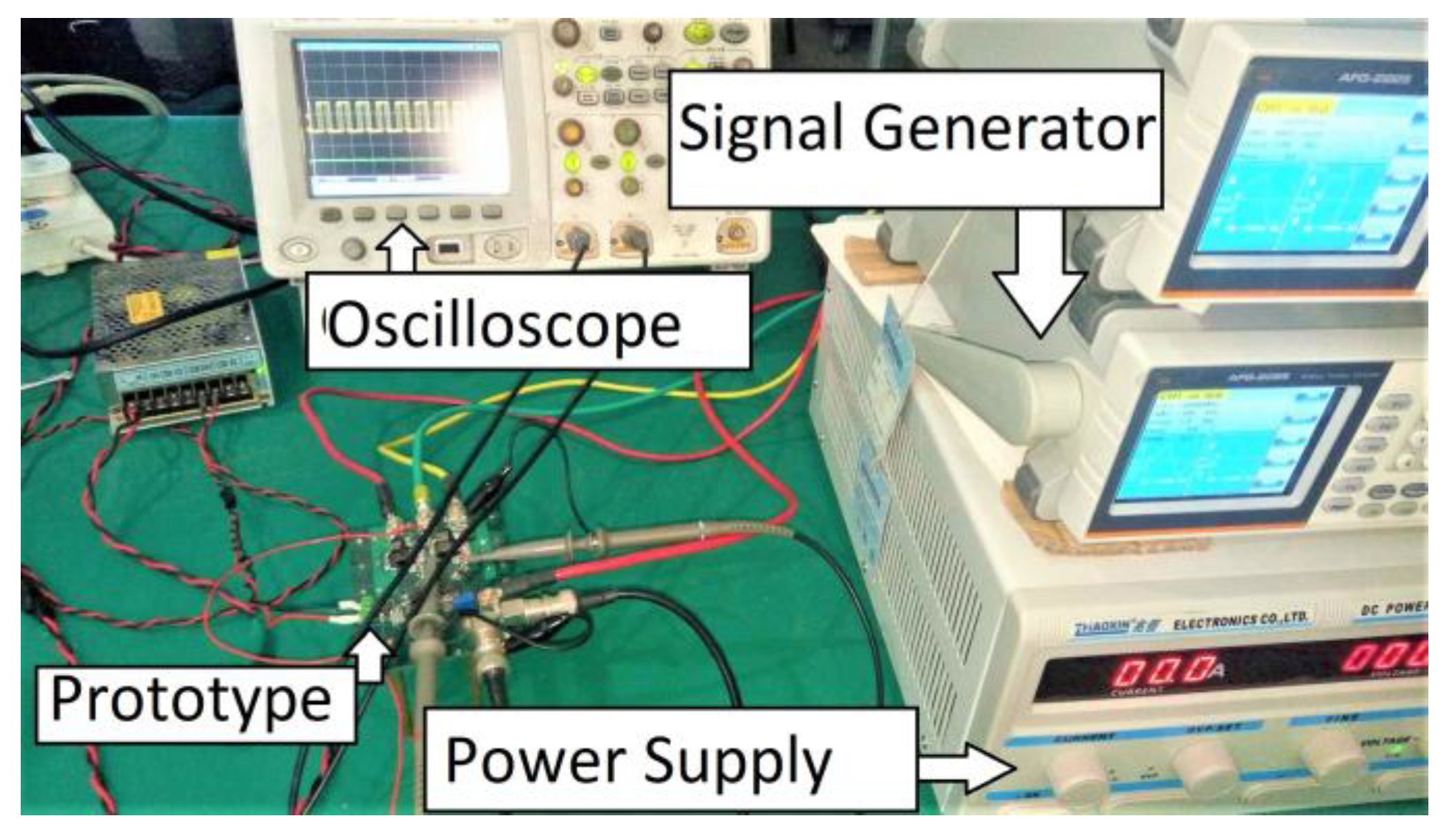
Figure 12 shows the setup of a half-bridge dc-ac converter for experimental verification. An isolated driver IC (Si8234) from Silicon Labs incorporation is used, which can operate at elevated frequencies, source and sink high gate current, and show significant immunity to EMI. Since the driver circuit traces carry a high-frequency signal, therefore, they are routed on the same layer to prevent the propagation of noise to other layers. Furthermore, to ensure Equation (24) [18], the driver circuit is routed using wide (25 mil) and shortest possible traces.
The symbol IR represents the rated current, gfs is the transconductance of SiC MOSFET, and LG is the parasitic gate inductance. Since the stray input capacitance is fixed, thereby, minimizing LG is effective in improving the damping of gate voltage resonance. In addition, a 10 kΩ gate-source resistor is connected, which is also useful in suppressing gate voltage oscillations.
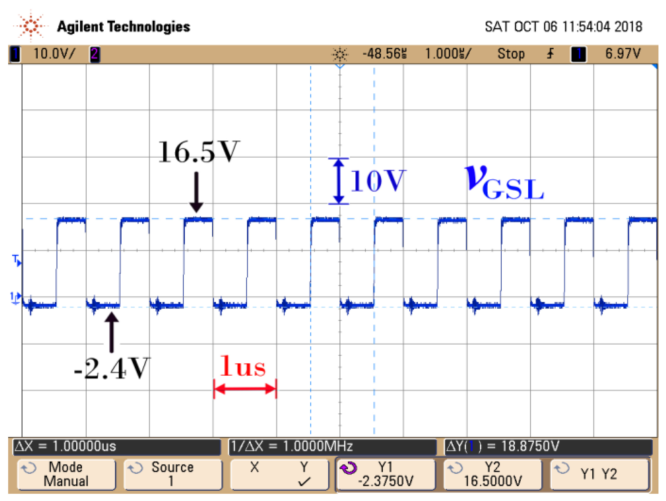
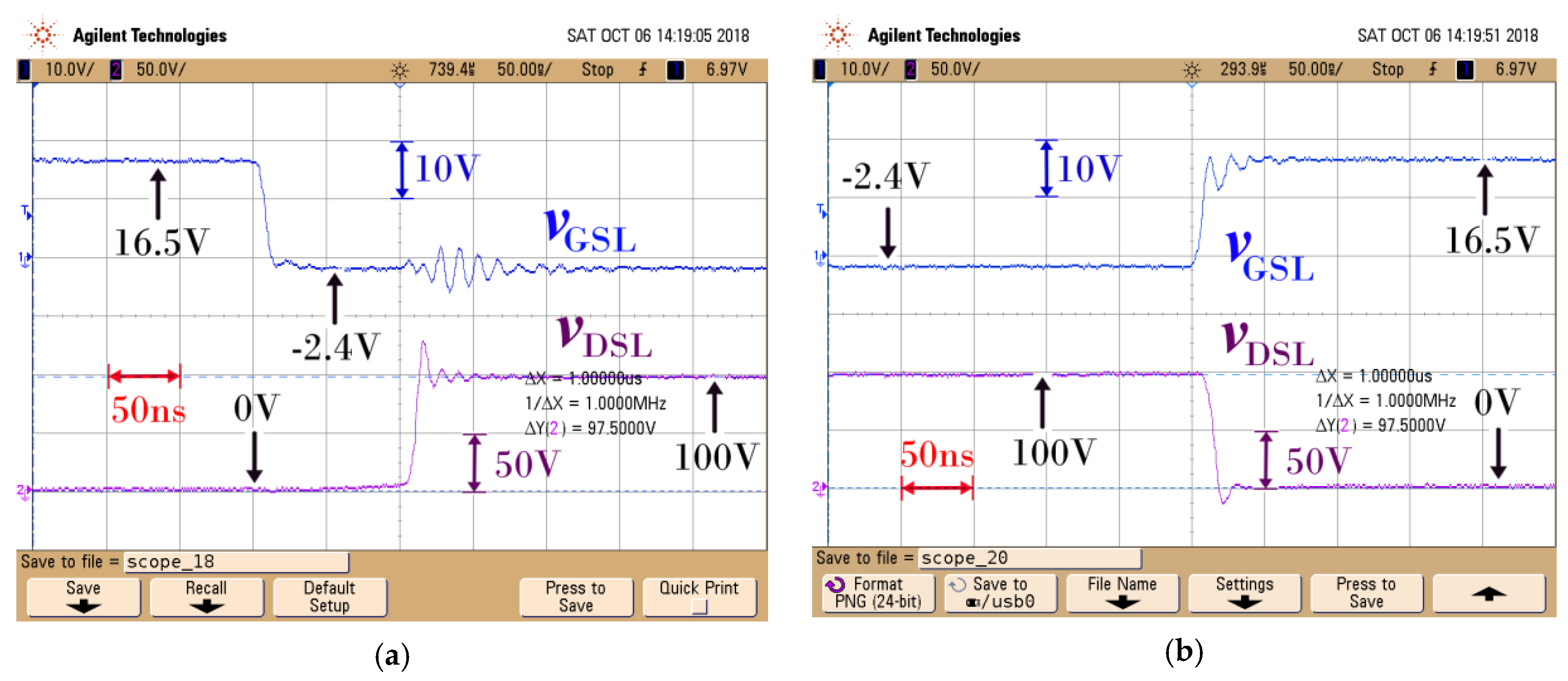
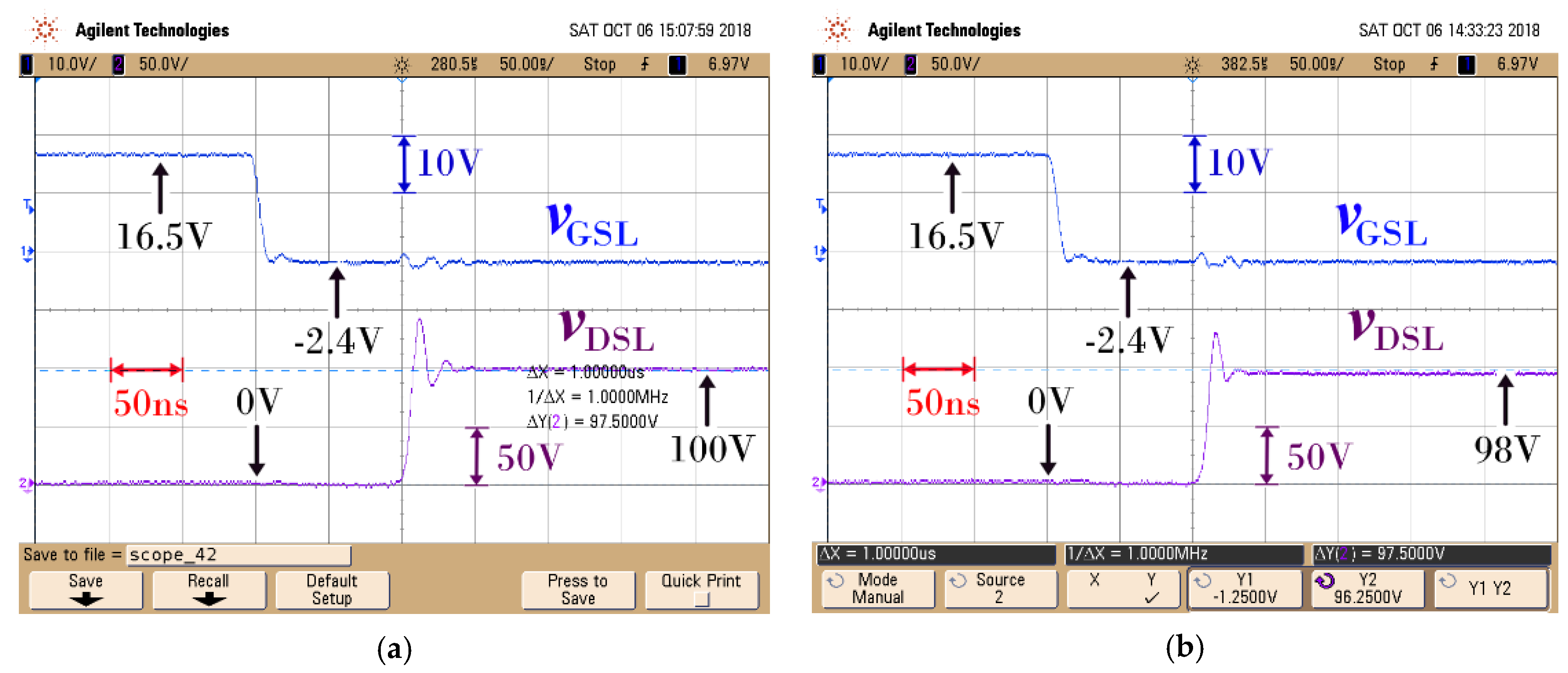
Figure 13 shows the experimental gate voltage waveform vGSL generated using the proposed gate driver at the 1 MHz switching frequency. The driver sets the turn-on and turn-off voltage to 16.5 V and −2.4 V respectively. The −2.4 V offset in gate voltage validates the basic level shifting capability of the gate driver. Moreover, Figure 14a,b show the turn-off and turn-on transition of the low-side MOSFET, respectively. Although, the spurious spike in gate-source voltage introduced by the fast-rising vDSL is below the gate threshold voltage, but the oscillations in vGSL are alarming due to the higher peaks. The ringing in vDSL due to circuit parasitics forces vGSL to oscillate, which can cause the crosstalk as well as stressing the device by exceeding the negative gate voltage limit. Therefore, RC snubber is used to dampen the parasitic ringing and thus increase the immunity to the crosstalk phenomenon and the gate breakdown. Figure 15 shows the gate-source and drain-source voltage waveforms of low-side MOSFET for two different RC snubbers. The waveform in Figure 15a shows the measured vDSL and vGSL when CSBR = 440 pF and RSBR = 10 Ω, resulting in a voltage overshoot of 41 V and settling time of 90 ns. For measurement of Figure 15b, CSBR has been raised to 1 nF, which reduces the voltage overshoot to 27 V and settling time to 54 ns. The results indicate that the assumption LSH = LDH = 0 leads to a mismatch between the experimental and mathematically derived parametric curves, and thus, the snubber selected using valley in the non-oscillatory region of Figure 8 is not viable. It is vital to choose high-valued RSBR to improve damping rather than CSBR to maintain relatively low power losses.
5.3. Limitations of the Proposed Gate Driver and the Snubber Design Technique
Although the proposed level shifter circuit relaxes the gate driver layout by getting rid of the additional negative voltage supply, but at the same time it relatively lowers the performance bar. The important concern is that the introduction of the capacitor CZL in the gate loop delays the turn-on transition of the SiC MOSFET. Moreover, vN requires several switching cycles at the start-up to rise up to the zener voltage VZ, and thus the negative turn-off voltage as determined by vN gradually increases in magnitude VZ. Finally, the negative voltage generated using the level shifter circuit is prone to parasitic oscillations, which can force gate voltage to exceed the negative limit, as a result overstressing the SiC MOSFET.
The snubber design technique presented in the paper predicts a region in the RSBR-CSBR plane where the switching ringing is suppressed. However, the accuracy of parasitic inductances and capacitances in the power loop determines the matching of the region derived using analytical equations with the experimental counterpart. Although, the manufacturer provides device specifications, but for computation of interconnection inductance, programs driven by the finite-element algorithm such as Maxwell 3D is required.
6. Conclusions
To improve the immunity against crosstalk phenomena, a gate driver has been proposed for SiC MOSFET capable of generating the negative turn-off voltage without using a negative power supply. Unlike the voltage divider based level shifters, the proposed circuit adds a negative offset to the gate-source voltage using reduced components with no additional resistor in the gate loop, thereby not affecting the efficiency. The effectiveness of the level shifter circuit has been validated by driving the SiC MOSFET in the half-bridge dc-ac converter at a switching frequency of 1 MHz which is 10 times higher than the RCD counterpart. Moreover, oscillation due to circuit parasitics are modeled, and guidelines for PCB layout to minimize the interconnection inductances are recommended. It is emphasized that due to unavoidable parasitic inductances, certain voltage ringing still exists which encourages passive damping. A procedure for the RC snubber design has been presented to avoid the trial and error based design. The snubber circuit has successfully lowered the gate voltage spike by 2.56 V and reduced the damping time by 63 ns.
Author Contributions
H.Z. and X.W. equally contributed to this paper. Conceptualization, H.Z. and X.W.; methodology, H.Z.; validation, H.Z. and S.K.; investigation, H.Z. and X.W.; resources, H.A.; data curation, S.K.; writing—original draft preparation, H.Z.; review and editing, X.Z., H.A. and X.W.; supervision, X.Z. and X.W.
Conflicts of Interest
There is no conflict of interest.
Nomenclature
| VIN | Source voltage |
| C | Output stage capacitor filter |
| C1/C2 | DC-link capacitors |
| L | Output stage inductor filter |
| R | Load resistance |
| fs/Ts | Switching frequency/switching time period |
| VTH | Threshold voltage |
| VMIL | Miller voltage |
| SL/SH | Low-side/high-side MOSFET of half-bridge converter |
| RONL/RONH | Conduction resistance of low-side/high-side MOSFET |
| CGSL/CGSH | Parasitic gate-source capacitance of low-side/high-side MOSFET |
| CDGL/CDGH | Parasitic drain-gate capacitance of low-side/high-side MOSFET |
| CDSL/CDSH | Parasitic drain-source capacitance of low-side/high-side MOSFET |
| LDL/LDH | Parasitic drain inductance of low-side/high-side MOSFET |
| LSL/LSH | Parasitic source inductance of low-side/high-side MOSFET |
| RGL(in)/RGH(in) | Internal gate resistance of low-side/high-side MOSFET |
| R1L/RTL | External gate turn-on/turn-off resistance of low-side MOSFET |
| DZPL/DZNL | Zener diode for positive/negative overvoltage gate protection |
| CZL/DZL | Capacitor/zener diode of the Level shifter circuit |
| vN/VZ | Voltage across CZL/zener voltage of DZL |
| VG | Gate driver supply voltage |
| LG | Parasitic gate inductance |
| vGSL/vGSH | Gate-source voltage of low-side/high-side MOSFET |
| vDSL/vDSH | Drain-source voltage of low-side/high-side MOSFET |
| iDL/iDH | Drain-source current of low-side/high-side MOSFET |
| iGPL/iGNL | Low-side gate current in turning-on/turning-off of MOSFET |
| iCL/iZL | Current through CZL/DZL |
| Dm | Maximum duty cycle |
| τa/τb | Time constant of gate loop during turn-on when (vN < VZ)/(vN = VZ) |
| τc | Time constant of gate loop during turn-off |
| iSBR/ISBR | Snubber current in time-domain/s-domain |
| gfs | transconductance of MOSFET |
| ωr/ζ | Parasitic resonance frequency/damping factor |
| RSBR/CSBR | Snubber resistor/capacitor |
| RC1/RC2 | Equivalent series resistance of C1/C2 |
| WBG | Wide band-gap devices |
| GaN | Gallium Nitride |
| SiC | Silicon carbide |
| THD | Total harmonic distortion |
| PCB | Printed circuit board |
| EMI | Electromagnetic interference |
| RC | Resistor-capacitor |
References
- Li, K.; Evans, P.; Johnson, M. SiC/GaN power semiconductor devices: a theoretical comparison and experimental evaluation under different switching conditions. IET Electr. Syst. Transp. 2018, 8, 3–11. [Google Scholar] [CrossRef] [Green Version]
- Jung, D.Y.; Park, Y. Design and Evaluation of Cascode GaN FET for Switching Power Conversion Systems. ETRI J. 2017, 39, 62–68. [Google Scholar] [CrossRef]
- Logan, T.; McMahon, R.; Hari, N. Design considerations for 600 V GaN cascode based half-bridge converter systems for utility based applications. In Proceedings of the 2016 IET International Conference on Power Electronics, Machine and Drives, Glasgow, UK, 19–21 April 2016; pp. 1–6. [Google Scholar]
- Yamaguchi, K.; Sasaki, Y.; Imakubo, T. Low loss and low noise gate driver for SiC-MOSFET with gate boost circuit. In Proceedings of the 2014 Annual Conference of the IEEE Industrial Electronics Society, Dallas, TX, USA, 29 October–1 November 2014; pp. 1594–1598. [Google Scholar]
- Peftitsis, D.; Rabkowski, J. Gate and Base Drivers for Silicon Carbide Power Transistors: An Overview. IEEE Trans. Power Electron. 2016, 31, 7194–7213. [Google Scholar] [CrossRef]
- Camacho, A.P.; Sala, V.; Ghorbani, H.; Martinez, J.L.R. A Novel Active Gate Driver for Improving SiC MOSFET Switching Trajectory. IEEE Trans. Ind. Electron. 2017, 64, 9032–9042. [Google Scholar] [CrossRef] [Green Version]
- Zeng, Z.; Li, X. Comparative Study on Multiple Degrees of Freedom of Gate Drivers for Transient Behavior Regulation of SiC MOSFET. IEEE Trans. Power Electron. 2018, 33, 8754–8763. [Google Scholar] [CrossRef]
- Wu, T. Cdv/dt induced turn-on in synchronous buck regulators. Int. rectifier Tech. Rep. 2007, 2, 2–7. [Google Scholar]
- Li, H.; Liao, X.; Hu, Y.; Huang, Z.; Wang, K. Analysis of voltage variation in silicon carbide MOSFETs during turn-on and turn-off. Energies 2017, 10, 1456. [Google Scholar] [CrossRef]
- Chen, H.; Divan, D. High speed switching issues of high power rated silicon-carbide devices and the mitigation methods. In Proceedings of the 2015 IEEE Energy Conversion Congress and Exposition, Montreal, QC, Canada, 20–24 September 2015; pp. 2254–2260. [Google Scholar]
- Zaman, H.; Zheng, X.; Yang, M.; Ali, H.; Wu, X. A SiC MOSFET based high efficiency interleaved boost converter for more electric aircraft. J. Power Electron. 2018, 18, 23–33. [Google Scholar]
- Liu, H.; Huang, X.; Lin, F.; Yang, Z. Loss Model and Efficiency Analysis of Tram Auxiliary Converter Based on a SiC Device. Energies 2017, 10, 2018. [Google Scholar] [CrossRef]
- Zheyu, Z.; Wang, F. Active gate driver for fast switching and cross-talk suppression of SiC devices in a phase-leg configuration. In Proceedings of the 2015 IEEE Applied Power Electronics Conference and Exposition, Charlotte, NC, USA, 15–19 March 2015; pp. 774–781. [Google Scholar]
- Abbatelli, L.; Brusca, C.; Catalisano, G. Application note: How to fine tune your SiC MOSFET gate driver to minimize losses. Available online: https://www.stmicroelectronics.com.cn/content/ccc/resource/technical/document/application_note/7d/2b/9d/f0/88/07/4b/6f/DM00170577.pdf/files/DM00170577.pdf/jcr:content/translations/en.DM00170577.pdf (accessed on 7 June 2017).
- Wang, J.; Chung, H.S.H. A novel RCD level shifter for elimination of spurious turn-on in the bridge-leg configuration. IEEE Trans. Power Electron. 2015, 30, 976–984. [Google Scholar] [CrossRef]
- Zhou, Q.; Gao, F.; Jiang, T. A gate driver of SiC MOSFET with passive triggered auxiliary transistor in a phase-leg configuration. In Proceedings of the 2015 Energy Conversion Congress and Exposition, Montreal, QC, Canada, 20–24 September 2015; pp. 7023–7030. [Google Scholar]
- Noppakunkajorn, J.; Han, D.; Sarlioglu, B. Analysis of high-speed PCB with SiC devices by investigating turn-off overvoltage and interconnection inductance influence. In Proceedings of the 2014 Applied Power Electronics Conference and Exposition, Fort Worth, TX, USA, 16–20 March 2014; pp. 2628–2634. [Google Scholar]
- Qin, H.; Ma, C.; Zhu, Z.; Yan, Y. Influence of parasitic parameters on switching characteristics and layout design considerations of SiC MOSFETs. J. Power Electron. 2018, 18, 1255–1267. [Google Scholar]
- Chen, Z.; Yao, Y.; Boroyevich, D.; Ngo, K.; Mattavelli, P. Exploration of a switching loop snubber for parasitic ringing suppression. In Proceedings of the 2014 IEEE Energy Conversion Congress and Exposition, Pittsburgh, PA, USA, 14–18 September 2014; pp. 1605–1612. [Google Scholar]
- Ren, Y.; Yang, X.; Zhang, F.; Tan, L.; Zeng, X. Analysis of a low-inductance packaging layout for Full-SiC power module embedding split damping. In Proceedings of the 2016 IEEE Applied Power Electronics Conference and Exposition, Long Beach, CA, USA, 20–24 March 2016; pp. 2102–2107. [Google Scholar]
- Palmer, P.R.; Zhang, J.; Zhang, X. SiC MOSFETs Connected in Series with Active Voltage Control. In Proceedings of the 2015 IEEE 3rd Workshop on Wide Bandgap Power Devices and Applications, Blacksburg, VA, USA, 2–4 November 2015; pp. 60–65. [Google Scholar]
- Huang, H.; Yang, X.; Wen, Y.; Long, Z. A switching ringing suppression scheme of SiC MOSFET by Active Gate Drive. In Proceedings of the 2016 IEEE 8th International Power Electronics and Motion Control Conference, Hefei, China, 22–26 May 2016; pp. 285–291. [Google Scholar]
- Han, D.; Sarlioglu, B. Comprehensive Study of the Performance of SiC MOSFET-Based Automotive DC-DC Converter under the Influence of Parasitic Inductance. IEEE Trans. Ind. Appl. 2016, 52, 5100–5111. [Google Scholar] [CrossRef]
- Li, L.; Ning, P.; Duan, Z.; Zhang, D.; Wen, X.; Qiu, Z. A study on the effect of DC-link decoupling capacitors. In Proceedings of the 2017 IEEE Transportation Electrification Conference and Expo, Asia-Pacific, Harbin, China, 7–10 August 2017; pp. 4845–4850. [Google Scholar]
- Kim, J.; Shin, D.; Sul, S.K. A Damping Scheme for Switching Ringing of Full SiC MOSFET by Air Core PCB Circuit. IEEE Trans. Power Electron. 2018, 33, 4605–4615. [Google Scholar] [CrossRef]
- Vaculik, P. The Experience with SiC MOSFET and Buck Converter Snubber Design. Int. J. Elect. Comput. Energ. Commun. 2014, 8, 49–54. [Google Scholar]
- Yatsugi, K.; Nomura, K.; Hattori, Y. Analytical Technique for Designing an RC Snubber Circuit for Ringing Suppression in a Phase-Leg Configuration. IEEE Trans. Power Electron. 2018, 33, 4736–4745. [Google Scholar] [CrossRef]
- Gao, F.; Zhou, Q.; Wang, P.; Zhang, C. A Gate Driver of SiC MOSFET for Suppressing the Negative Voltage Spikes in a Bridge Circuit. IEEE Trans. Power Electron. 2018, 33, 2339–2353. [Google Scholar] [CrossRef]
- Nayak, P.; Krishna, M.V.; Vasudevakrishna, K.; Hatua, K. Study of the effects of parasitic inductances and device capacitances on 1200 V, 35 A SiC MOSFET based voltage source inverter design. In Proceedings of the 2014 IEEE International Conference on Power Electronics, Drives and Energy Systems, Mumbai, India, 16–19 December 2014; pp. 1–6. [Google Scholar]
- Wang, Z.; Zhang, J.; Wu, X.; Sheng, K. Analysis of stray inductance’s influence on SiC MOSFET switching performance. In Proceedings of the 2014 IEEE Energy Conversion Congress and Exposition, Pittsburgh, PA, USA, 14–18 September 2014; pp. 2838–2843. [Google Scholar]
- Han, D.; Lee, W.; Noppakunkajorn, J.; Sarlioglu, B. Investigating the influence of interconnection parasitic inductance on the performance of SiC Based DC-DC converters in hybrid vehicles. In Proceedings of the 2014 IEEE Transportation Electrification Conference and Expo, Dearborn, MI, USA, 15–18 June 2014; pp. 1–7. [Google Scholar]
- Anthon, A.; Hernandez, J.C.; Zhang, Z.; Andersen, M.A.E. Switching investigations on a SiC MOSFET in a TO-247 package. In Proceedings of the 2014 Conference of the IEEE Industrial Electronics Society, Dallas, TX, USA, 29 October–1 November 2014; pp. 1854–1860. [Google Scholar]
- White Paper. Optimizing PCB Layout. 2014. Available online: https://epc-co.com/epc/Portals/0/epc/documents/papers/Optimizing%20PCB%20Layout%20with%20eGaN%20FETs.pdf (accessed on 7 June 2017).
- Application Note. PCB Layout Considerations for Non-Isolated Switching Power Supplies. Available online: https://www.analog.com/media/en/technical-documentation/application-notes/an136f.pdf (accessed on 7 June 2017).
- Application Note. Thermal Considerations for a Class D Amplifier 2006. Available online: https://www.maximintegrated.com/en/app-notes/index.mvp/id/3879 (accessed on 7 June 2017).
- Application Note. RC Snubber for Class-D Audio Amplifiers 2018. Available online: https://statics.cirrus.com/pubs/appNote/AN0454REV1.pdf (accessed on 7 June 2017).
- Application Note. Snubber Circuits for Power Electronics 2008. Available online: https://rudys.typepad.com/files/snubber-e-book-complete.pdf (accessed on 7 June 2017).
- Wang, X.; Shi, J.; Li, T.; Sun, Y. Active closed-loop gate voltage control method to mitigate metal-oxide semiconductor field-effect transistor turn-off voltage overshoot and ring. IET Power Electron. 2013, 6, 1715–1722. [Google Scholar] [CrossRef]
- Torsaeter, B.N.; Tiwari, S.; Lund, R.; Midtgard, M. Experimental evaluation of switching characteristics, switching losses and snubber design for a full SiC half-bridge power module. In Proceedings of the 2016 IEEE 7th International Symposium on Power Electronics for Distributed Generation Systems, Vancouver, BC, Canada, 27–30 June 2016; pp. 1–8. [Google Scholar]
Figure 1.
(a) Equivalent circuit of the SiC MOSFET based half-bridge dc-ac converter with the parasitic components (b) illustration of voltage spike during turn-on transition of high-side MOSFET.
Figure 1.
(a) Equivalent circuit of the SiC MOSFET based half-bridge dc-ac converter with the parasitic components (b) illustration of voltage spike during turn-on transition of high-side MOSFET.

Figure 2.
Gate driver for SiC MOSFET with (a) RCD level shifter [15] (b) voltage divider based level shifter [28].

Figure 3.
(a) The proposed gate driver for SiC MOSFET, and equivalent circuits during (b) turning-on transition and (c) turning-off.
Figure 3.
(a) The proposed gate driver for SiC MOSFET, and equivalent circuits during (b) turning-on transition and (c) turning-off.

Figure 4.
Switching waveforms of the proposed gate driver.

Figure 5.
(a) Equivalent circuit of the half-bridge converter during overlap conduction (b) equivalent circuit when the SL turn-off.
Figure 5.
(a) Equivalent circuit of the half-bridge converter during overlap conduction (b) equivalent circuit when the SL turn-off.

Figure 6.
Effect of parasitic inductance on the drain current iDL and gate-source and drain-source voltage waveforms.
Figure 6.
Effect of parasitic inductance on the drain current iDL and gate-source and drain-source voltage waveforms.

Figure 7.
(a) half-bridge dc-ac converter with RC snubber (b) Equivalent circuit using high-frequency assumption.
Figure 7.
(a) half-bridge dc-ac converter with RC snubber (b) Equivalent circuit using high-frequency assumption.

Figure 8.
The parametric graph of snubber with the region where oscillation is suppressed.

Figure 9.
Switching waveform captured from simulation (a) during turn-on of low-side MOSFET (b) during turn-off of low-side MOSFET.
Figure 9.
Switching waveform captured from simulation (a) during turn-on of low-side MOSFET (b) during turn-off of low-side MOSFET.

Figure 10.
(a) Gate-source voltage of low-side MOSFET under different R1L values (b) relationship between R1L and spurious peak voltage.
Figure 10.
(a) Gate-source voltage of low-side MOSFET under different R1L values (b) relationship between R1L and spurious peak voltage.

Figure 11.
Simulation results of voltage ringing for different snubber cases (a) CSBR = 1 nF and RSBR = 3, 6 and 10 Ω (b) RSBR = 1 Ω and CSBR = 0.47, 2.2 and 4.7 nF.
Figure 11.
Simulation results of voltage ringing for different snubber cases (a) CSBR = 1 nF and RSBR = 3, 6 and 10 Ω (b) RSBR = 1 Ω and CSBR = 0.47, 2.2 and 4.7 nF.

Figure 12.
Experimental setup of the half-bridge dc-ac converter with the proposed gate driver.

Figure 13.
Experimental gate-source voltage waveform of low-side MOSFET.

Figure 14.
Experimental switching waveforms without snubber (a) turn-off, and (b) turn-on of low-side SiC MOSFET.
Figure 14.
Experimental switching waveforms without snubber (a) turn-off, and (b) turn-on of low-side SiC MOSFET.

Figure 15.
Experimental turning-on waveforms with RC snubber using (a) CSBR = 440 pF and RSBR = 10 Ω, and (b) CSBR = 1 nF and RSBR = 10 Ω.
Figure 15.
Experimental turning-on waveforms with RC snubber using (a) CSBR = 440 pF and RSBR = 10 Ω, and (b) CSBR = 1 nF and RSBR = 10 Ω.


Table 1.
Specifications of the SiC MOSFET based half-bridge dc-ac converter.
| Parameter | Value |
|---|---|
| Source voltage (VIN) | 100 V |
| Capacitor (C) | 1.5 µF |
| Inductor (L) | 33 µH |
| Load Resistance (R) | 10 Ω |
| Switching frequency (fs) | 1 MHz |
Table 2.
Parameters of the C3M0120090J.
| Parameter | Value |
|---|---|
| Threshold voltage | 2.1 V |
| Intrinsic gate resistance | 16 Ω |
| Maximum gate-source voltage | −8/+18 |
| Input capacitance | 350 pF |
| Output capacitance | 40 pF |
| Reverse transfer capacitance | 3 pF |
Table 3.
Parameters of the proposed gate driver.
| Parameter | Value |
|---|---|
| R1L | 3 Ω |
| R2L | 3 Ω |
| DZPL | 18 V |
| DZNL | 5 V |
| CZL | 1 µF |
© 2018 by the authors. Licensee MDPI, Basel, Switzerland. This article is an open access article distributed under the terms and conditions of the Creative Commons Attribution (CC BY) license (http://creativecommons.org/licenses/by/4.0/).
Share and Cite
MDPI and ACS Style
Zaman, H.; Wu, X.; Zheng, X.; Khan, S.; Ali, H. Suppression of Switching Crosstalk and Voltage Oscillations in a SiC MOSFET Based Half-Bridge Converter. Energies 2018, 11, 3111. https://doi.org/10.3390/en11113111
AMA Style
Zaman H, Wu X, Zheng X, Khan S, Ali H. Suppression of Switching Crosstalk and Voltage Oscillations in a SiC MOSFET Based Half-Bridge Converter. Energies. 2018; 11(11):3111. https://doi.org/10.3390/en11113111
Chicago/Turabian StyleZaman, Haider, Xiaohua Wu, Xiancheng Zheng, Shahbaz Khan, and Husan Ali. 2018. "Suppression of Switching Crosstalk and Voltage Oscillations in a SiC MOSFET Based Half-Bridge Converter" Energies 11, no. 11: 3111. https://doi.org/10.3390/en11113111
Note that from the first issue of 2016, this journal uses article numbers instead of page numbers. See further details here.