Efficiency Optimization of a Variable Bus Voltage DC Microgrid


Department of Electrical, Electronic, and Automatic Control Engineering, Universitat Rovira i Virgili, 43007 Tarragona, Spain
*
Authors to whom correspondence should be addressed.
Energies 2018, 11(11), 3090; https://doi.org/10.3390/en11113090
Submission received: 28 September 2018
/
Revised: 30 October 2018
/
Accepted: 5 November 2018
/
Published: 8 November 2018
(This article belongs to the Special Issue Control and Nonlinear Dynamics on Energy Conversion Systems)
Abstract
:A variable bus voltage DC microgrid (MG) is simulated in Simulink for optimization purposes. It is initially controlled with a Voltage Event Control (VEC) algorithm supplemented with a State of Charge Event Control (SOCEC) algorithm. This control determines the power generated/consumed by each element of the MG based on bus voltage and battery State of Charge (SOC) values. Two supplementary strategies are proposed and evaluated to improve the DC-DC converters’ efficiency. First, bus voltage optimization control: a centralized Energy Management System (EMS) manages the battery power in order to make the bus voltage follow the optimal voltage reference. Second, online optimization of switching frequency: local drivers operate each converter at its optimal switching frequency. The two proposed optimization strategies have been verified in the simulations.
1. Introduction
Electric power transmission network’s topology is being rethought and reformulated nowadays. Ecological, social and economic perspectives recommend moving towards grid decentralization. According to [1], distributed generation provides a range of benefits, including:
- Generation, transmission, and distribution capacity investments deferral.
- Ancillary services.
- Environmental emissions benefits.
- System losses reduction.
- Energy production savings.
- Reliability enhancement.
Development of microgrids is part of the new grid model. A microgrid (MG) consist of a number of interconnected and coordinated elements: generator(s), load(s), energy storage(s) and electrical grid. In DC microgrids, all these elements are connected to a common DC bus through individual DC-DC converters. Power management of the different elements of a MG is necessary to guarantee that the system operates always stable and that, whenever possible, Renewable Energy Sources (RES) operate at their Maximum Power Point (MPP) and critical loads are supplied.
Adequate management of the power of MG’s elements is a key to accomplishing stable operation, improving energy efficiency, extending battery lifetime and achieving maximum economic yield.
MG stable operation require to coordinately control all the MG’s elements. Control algorithms for microgrids, following [2], can be divided into three categories from the communication perspective:
- Decentralized control: Digital Communication Links (DCL) do not exist and power lines are used as the only channel of communication. It is generally based on the interpretation of the voltage in the common DC bus.
- Centralized control: Data from distributed units are collected in a centralized aggregator, processed and feedback commands are sent back to them via DCLs.
- Distributed control: DCLs are implemented between units and coordinated control strategies are processed locally.
Droop control [3,4] is the basic diagram for decentralized control. In DC microgrids, primary droop control achieves power sharing among the parallel connected sources and bidirectional DC-DC converters. The control of each converter locally determines the power that it must perform according to a linear control law based on the bus voltage. Droop control changes the power reference of the sources’ converters as the bus voltage varies due to variations in load or generation. For example, starting from a stable operation point, if load increases, bus voltage tends to decrease. This makes the decentralized control system increase the power supplied by each source according to its particular linear control law. Larger sources contribute with more power thanks to the different droop coefficients for different units. Bus voltage can be restored to its initial value implementing secondary and tertiary droop control. However, only primary droop control is utilized in the MG studied in this paper.
Besides stable operation, more advanced control strategies enable to improve the MG performance. Most MG management optimization studies focus on finding out the optimal economic dispatch. Some examples are summarized next. In [3], an optimization problem is formulated to achieve load sharing minimizing fuel and operation costs. In [5], a multi–objective optimization function is utilized to balance the tradeoff between maximizing the MG revenue and minimizing the MG operation cost, including penalties for bid deviation, renewable energy curtailment, and involuntary load shedding. In [6], a genetic algorithm solves an optimization problem to minimize the instantaneous (no forecasting is considered) MG total operation cost, taking into account real-time pricing of electricity from the utility grid. In [7], a genetic algorithm is implemented to minimize the daily net cost of the Battery Energy Storage System (BESS) scheduling. In [8], a genetic algorithm schedule is used to minimize economic operation cost, including demand response price policy in the model. In [9], a linear optimization problem is solved to determine the day ahead and intraday markets bids that maximize the overall profits of a photovoltaic plant with BESS, considering battery aging, incomes and penalties due to provision of ancillary services and forecast uncertainty.
This paper presents a DC microgrid managed in a stable manner by an Events–Based Control System, and proposes two strategies for efficiency optimization, rather than economic optimization, which has been more frequently addressed. The two proposed strategies are:
- Bus Voltage Optimization Control (BVOC).
- Online Optimization of Switching Frequency (OOSF).
The objective of both strategies is to minimize the DC-DC converters’ losses. The proposed optimization algorithms are compatible with economic optimization strategies.
To the best of the authors’ knowledge, online bus voltage optimization of a DC microgrid has never been addressed. The most similar study to BVOC optimization found is [10], which determines optimal bus voltages for residential and commercial DC MGs applications. In this case, though, the optimal voltages are constant, so it provides a design criterion rather than an online optimization algorithm. In [11,12], bus voltage control is addressed with different approaches, namely, double loop PI control and droop coefficients optimization, but considering a fixed and predetermined bus voltage level in both cases.
Switching frequency optimization of individual DC-DC converters has been previously modeled in [13,14,15,16] and implemented online in [17,18,19].
After providing basic background on microgrids’ management and optimization in this introduction, the sections below are organized as follows. In Section 2, a simulated variable bus voltage MG is described, as well as its existing control algorithm based on bus voltage and State of Charge events. Afterwards, the efficiency curves of the MG’s converters are analyzed in detail in Section 3. In sections four and five, the aforementioned efficiency optimization strategies, Bus Voltage Optimization Control and Online Optimization of Switching Frequency, are explained thoroughly. In Section 6, the MG is simulated implementing both BVOC and OOSF, and their performance and dynamic evolution are evaluated. Section 7, finally, contains the summarization and discussion of the results.
2. Description of the MG Studied
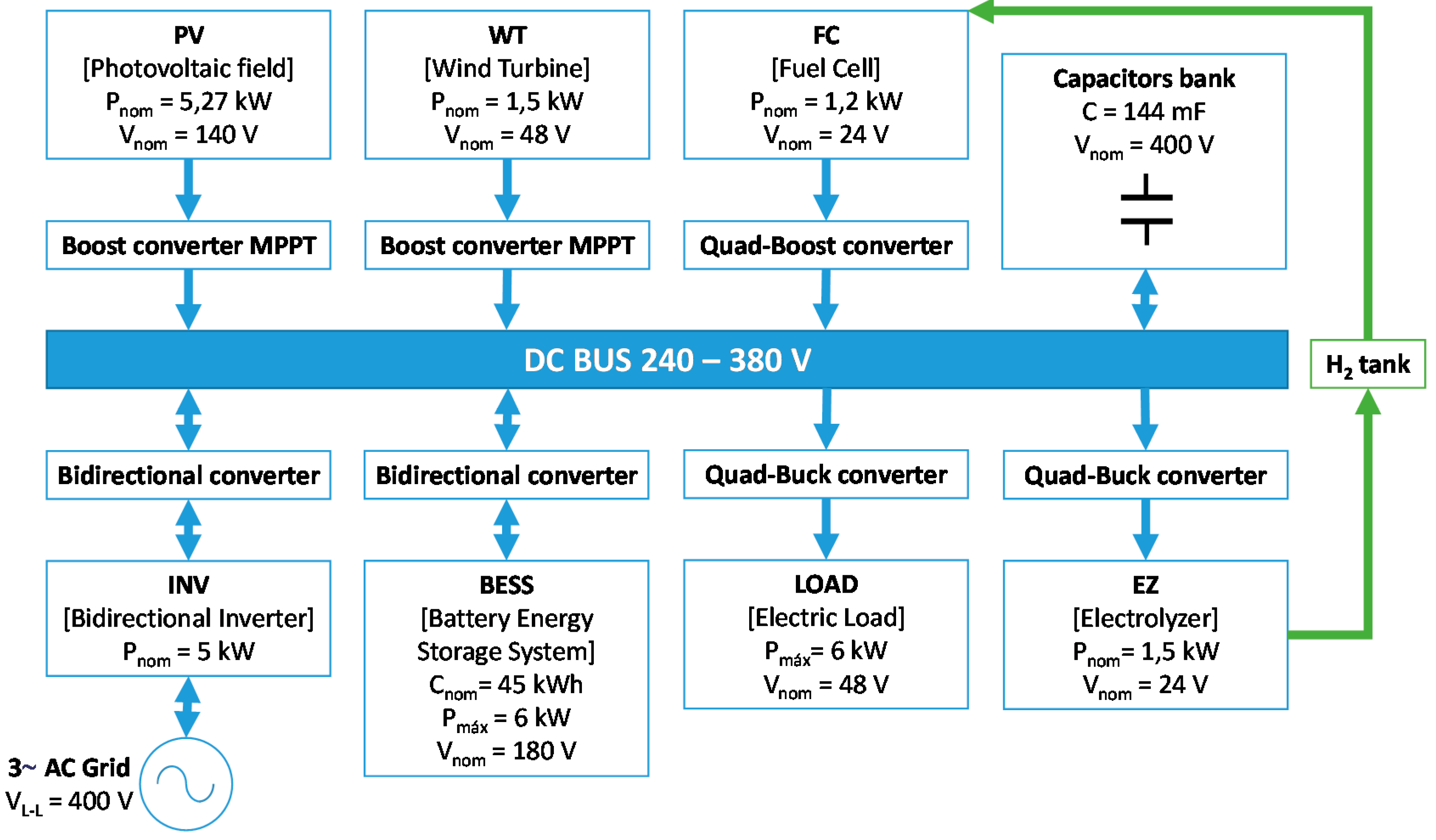
The MG studied is simulated in Simulink [20] and it is based on the MG described in [21]. The MG’s elements are listed in Table 1.
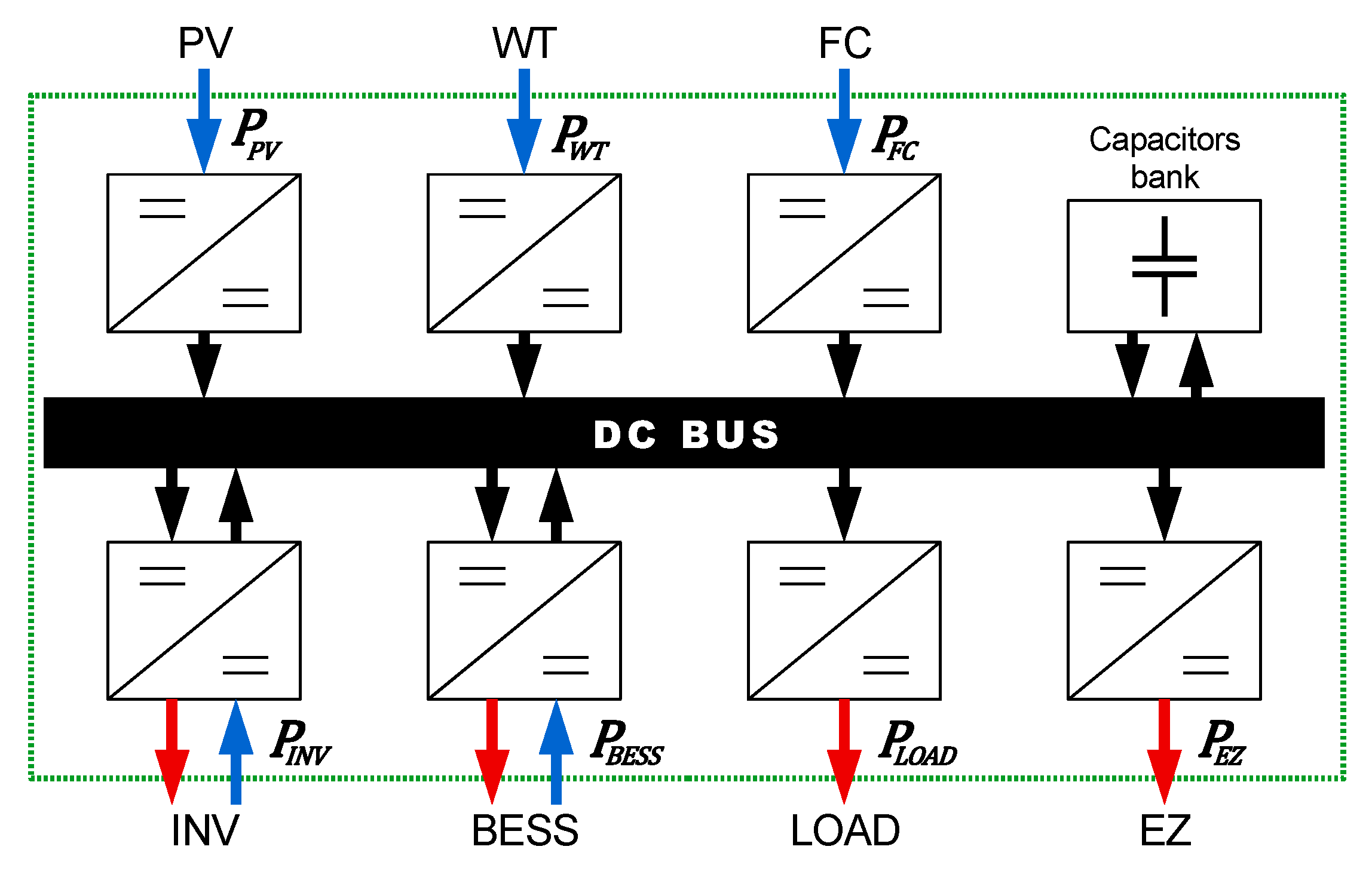
Figure 1 shows the MG’s elements interconnected in a variable voltage DC bus through DC-DC converters and the topology chosen for each of them. All the MG’s converters are controlled as power sources. Converters with nominal power over 3 kW have been designed with IGBTs while those with lower nominal power have been designed with MOSFETs. It has been imposed an inductor current ripple lower than 20% in the worst-case scenario: nominal operating conditions and minimum switching frequency (3 kHz for IGBT converters and 20 kHz for MOSFET converters). The transistors operate hard switching in continuous conduction mode. Averaged models of the converters’ losses based on small-signal analysis have been employed. The converters are modeled considering conduction and switching losses, following [22,23]. Average current values are used, since the error is small thanks to the low current ripple.
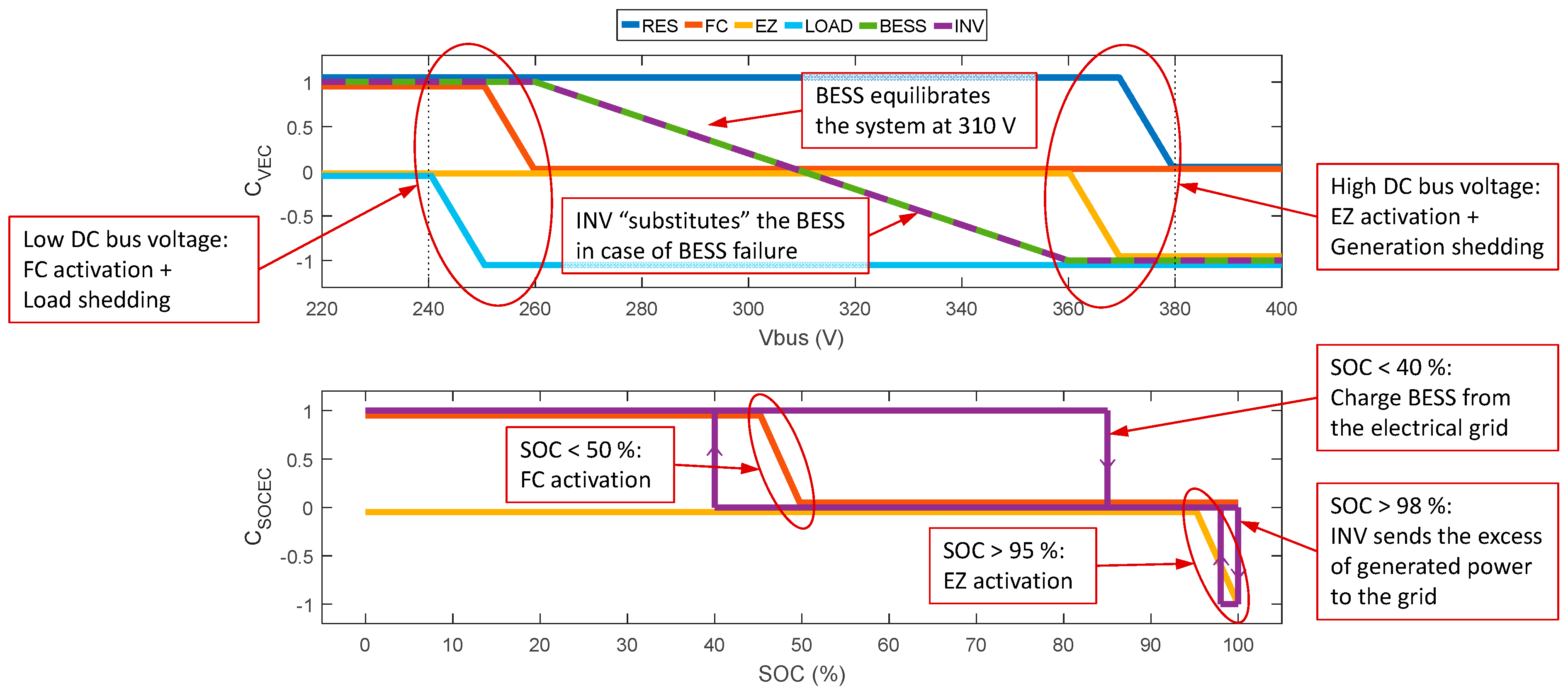
The existing MG’s control system consists of a decentralized Voltage Event Control (VEC) in every unit, supplemented with a State of Charge Event Control (SOCEC) in FC, EZ and INV. This initial control system will be denominated Events-Based Control System (E-BCS = VEC + SOCEC). VEC is a primary droop control using no secondary or tertiary droop control to stabilize bus voltage.
Each unit follows its correspondent linear control law based on the bus voltage (). FC, EZ and INV also follow their additional control laws based on the battery State of Charge (SOC).
The E-CBS determines a coefficient that multiplies the absolute value of the available/demanded/nominal power of the source/load/bidirectional unit . The coefficient value is the saturated sum of VEC coefficient plus SOCEC coefficient , as shown in Equation (1). The coefficients and are defined in Figure 2. The power reference imposed in the converter is calculated as in Equation (2). The sign convention is: is positive if the power is coming into the DC bus and negative is power is coming out:
is the maximum power that a RES can generate at a given moment; is the nominal power of the source/load/bidirectional unit ; and is the load’s electricity demand.
Voltage limitations are established in 240 V ≤ ≤ 380 V. The lower limit is chosen such that always remains above the maximum PV voltage (190 V approx.) and the maximum BESS voltage (220.5 V). This permits to discard the use of buck-boost and bidirectional buck-boost converters, which are less efficient than the finally selected PV’s boost converter and BESS’ bidirectional converter (see Figure 1). The higher voltage limit is the result of applying a safety margin with respect to the maximum voltage of the capacitors bank (400 V). A 20 V safety margin is sufficient thanks to the robustness of E-CBS maintaining voltage peaks lower than this value.
Voltage Event Control algorithm manages power balance, in order to keep the system stable. Power from Renewable Energy Sources (RES) (i.e., PV and WT) is limited when is too high (over 370 V). LOAD power is limited when is too low (under 250 V)—this can only happen if the MG operates in islanded mode and with fully discharged battery. BESS power tends to equilibrate the system at the medium voltage level (i.e., 310 V). FC and EZ are utilized as emergency support source/load when approaches the lower/higher voltage limit.
FC, EZ and INV also incorporate State of Charge Event Control: an independent power control based on battery SOC that, on the one hand, avoids performing deep discharges and, on the other, avoids missing RES generation when SOC ≈ 100%. Hydrogen production/consumption are activated when the SOC reaches high (95%)/low (50%) values. The inverter will follow the BESS control law in case of BESS failure or when SOC exceeds 98%; and will deliver full power to the DC bus when SOC drops down to 40%. All the linear control laws apply simultaneously, except the INV VEC control law (dashed line), which only applies in case of BESS failure.
MG’s operation controlled by E-BCS is taken as the reference to assess Bus Voltage Optimization Control (BVOC) and Online Optimization of Switching Frequency (OOSF) performances. The power that each source/load/bidirectional converter has to deliver is determined by E-BCS. When BVOC is implemented, it substitutes the E-BCS control (only) in the BESS’ converter. The rest of the converters maintain their VEC and SOCEC control laws, except for FC and EZ VEC control laws, which only regulate FC and EZ powers in some specific cases. BVOC controller calculates BESS power as the power that makes the bus voltage reach its optimal value. OOSF, in its turn, does not affect the power reference of any of the MG’s converters—OOSF locally optimizes the switching frequency of the converters in which it is applied, while their power references remain unaltered. Thus, the power references in all the MG’s converters are imposed by E-BCS, except when BVOC is implemented, that it modifies the BESS’ converter power reference.
3. Analysis of the Energy Efficiency Curves of the DC-DC Converters
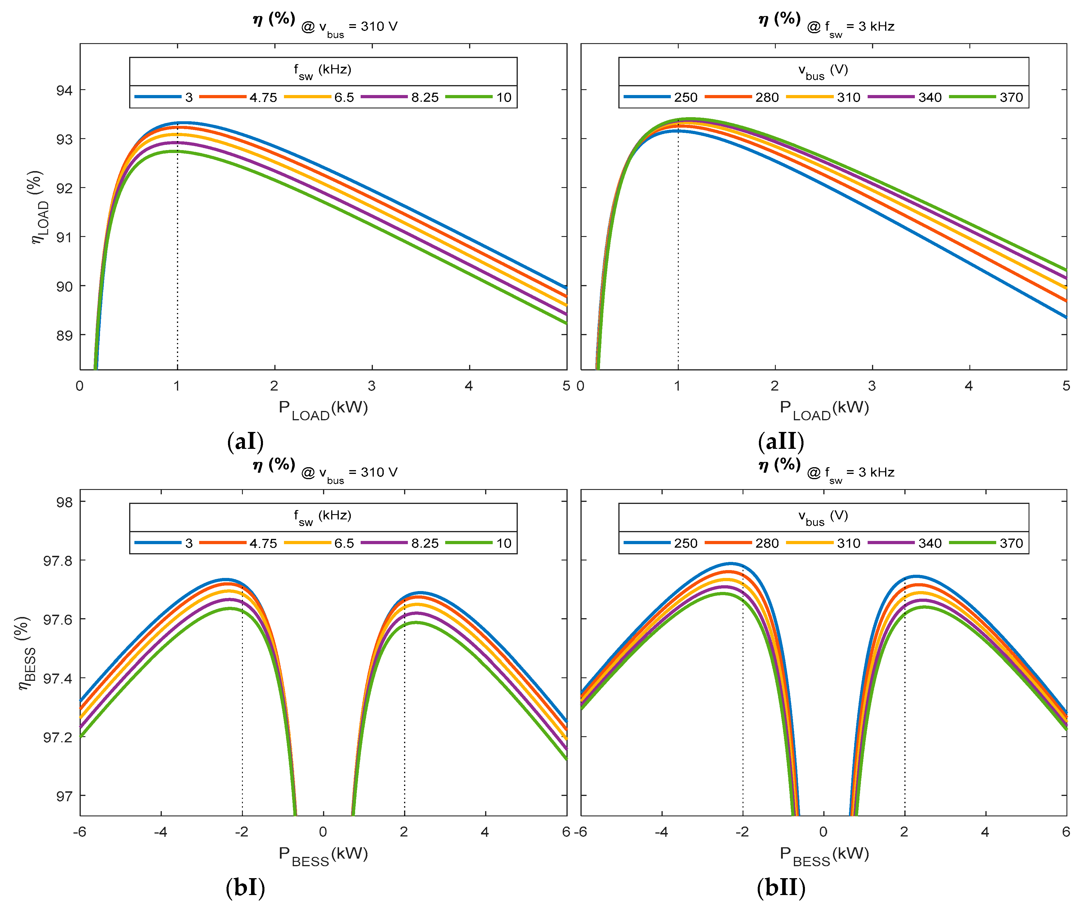
Figure 3 shows the efficiency curves of two representative converters of the seven MG’s DC-DC converters (LOAD’s and BESS’ converters) operating at different switching frequencies and bus voltage values. In this section, these curves are analyzed to anticipate the order of magnitude of the efficiency improvement that the two proposed optimization strategies BVOC and OOSF will produce.
The efficiency curves of the LOAD’s and BESS’ converters (which are quadratic buck and bidirectional converters, respectively, as can be seen in Figure 1) have been chosen because they serve to illustrate general issues that occur in all the MG’s converters, namely:
- First, there is little room for energy efficiency improvement for both optimization strategies. The efficiency curves reveal small efficiency differences within the studied range of possible and values. Efficiency increases are limited to a fraction of a percentage point.
- Second, the optimal bus voltage is different for individual converters. Thus, a change in leading to catch up with the overall optimal bus voltage , causes some of the MG’s converters to operate more efficiently but, also, it causes some other converters to operate less efficiently. The overall effect is that BVOC achieves efficiency improvements, yet low ones for this reason.
Figure 3(aI) shows the efficiency curves of the LOAD’s quadratic buck converter for five values of switching frequency, linearly distributed within the range 3–10 kHz, at a constant bus voltage of 310 V. The Online Optimization of Switching Frequency algorithm applies to each converter individually, so they all will operate at their optimal switching frequency (the highest curve in the graph). OOSF controls the gate driver of the transistors to operate them at optimal switching frequency (i.e., 3 kHz, blue curve, for most values). The efficiency of the LOAD converter increases steeply from = 0 kW to 1 kW approx. In this first part of the curve, it is possible to obtain significant efficiency improvements in relative terms, but with low impact in absolute terms. In the second part of the curve, from = 1 kW to 5 kW, the maximum possible efficiency improvement remains constant with a value of 0.75%. Figure 3(bI) is essentially the same graph but with the efficiency curves of the BESS’s bidirectional DC-DC converter. The left half of the graph ( < 0 kW) represents the buck operation mode; the right part represents the boost operation mode. The turning points where the slope changes sharply occur at = ±2 kW approx. The maximum possible efficiency improvement for high is as low as 0.12% in this case.
Figure 3(aII) shows the efficiency curves of the LOAD quadratic buck converter for five bus voltage levels, linearly distributed within the range 250–370 V, at a constant switching frequency of 3 kHz. BVOC regulates the duty cycle of the transistors in order to operate the MG at optimal bus voltage, which minimizes the losses of the set of DC-DC converters taken as a whole. This optimization algorithm is applied globally, so, in general, global optimum will not coincide with local optimums. In this curve, the efficiency of the LOAD converter increases steeply also from = 0 kW to 1 kW approx. For power greater than 1 kW, the maximum possible efficiency improvement steadily increases from 0.23% at 1 kW to 0.96% at 5 kW. Figure 3(bII) is again the same graph but representing the BESS’ bidirectional DC-DC converter. The maximum possible efficiency improvement for high values of is as low as 0.06% in this case.
Figure 3(aII,bII) show that, in general, local optimums for different MG’s units occur at opposed increments: for example, if > 1 kW, raising makes the efficiency of LOAD’s converter increase but, at the same time, it makes the efficiency of BESS’ converter decrease (and vice versa), regardless of what the is. Optimum bus voltage reference calculated by BVOC is the trade-off that minimizes the sum of power losses in all the converters. Hence, not all of them will operate simultaneously at their local optimum point in general.
4. Bus Voltage Optimization
This first optimization approach, Bus Voltage Optimization Control (BVOC), makes use of the distinctive varying DC bus voltage characteristic of the MG to online improve the efficiency of the set of MG’s converters taken as a whole, for all the possible power flows.
The power of the MG’s sources, loads and bidirectional units continuously varies so individual optimization of the converters at their rated power is not an adequate approach in MG applications. Global optimization, considering all the possible power flows (i.e., all the possible operation points of the converters) is conducted next.
BVOC controls the BESS power substituting the VEC control law (shown in Figure 2) in the BESS’ converter. RES’s, LOAD’s and INV’s converters maintain their E-BCS control laws. FC’s and EZ’s converters maintain their SOCEC control laws; but their VEC control laws only apply if one of the following three conditions is met: BVOC controller failure, energy shortage or energy excess.
BVOC keeps the bus voltage at its optimal value in every moment. The calculation variable is used in the system of equations of the BVOC optimization problem (in capital letters to differentiate between , this calculation variable, and , which represents the bus voltage not as a calculation variable, but as the real, measurable, physical magnitude). The optimal bus voltage is defined here as the value of the calculation variable that minimizes the sum of the converters’ losses () for the instantaneous power flows among the MG’s units. A centralized Energy Management System (EMS) calculates online every 100 ms, evaluating a –dependent deterministic model of explained below. With the reference , a PI controller determines the power that the BESS must perform to make catch up with .
From now on, this optimization strategy will be denoted by BVOCBESS, to highlight that this control algorithm applies only to the BESS converter, while the remaining converters maintain the E-BCS presented in the previous section.
The EMS gathers sensor readings of switching frequencies, and input and output voltages and currents from all the converters. With them, the EMS evaluates an online loss models of all the converters. The Matlab [20] function fminbnd is used to solve the nonlinear optimization problem formulated in Equations (3) and (4). It returns the value of the calculation variable that is a minimizer of the sum of the converters’ losses (), within the interval in which both load and RES remain unconstrained, i.e., 250 V–370 V:
where is the sum of the —dependent expressions of power loss () in the converters of each unit , given their measured switching frequencies (), powers () and voltages (). Measured values get updated every 100 ms. Notice that and are dependent on .
In order to clarify how the EMS calculates , an example is provided: the power loss equations of one of the DC-DC converters, which is one of the seven addends in Equation (4). PV boost converter’s power loss () is calculated evaluating the Equations (5)–(7). Note that the remaining expressions (see Appendix A) are analogous and must be added up to according to Equation (4), to calculate the total power loss as a function of and obtain the that minimizes it:
where is the converter’s efficiency; , , and are the measured output and input voltages and currents (note that is the measured value of ); is the transistor’s duty cycle (the value of in Equation (6) is considered equal to that of Equation (5) during each time step; the value of gets corrected every time step as the measured gets updated, and so does the value of ); is the inductor resistance; is the flux density ripple calculated using the Faraday’s Law, see [24]; are the characteristic parameters of the inductor’s magnetic core; is the actual switching frequency; are the resistance and the forward voltage drop of the diode; are the resistance and the forward voltage drop of the IGBT; and is the sum of transition turn–on and turn–off times of the IGBT. Notice that , , and are dependent on . The full system of equations and list of parameters is provided in the Appendix A.
BVOCBESS achieves two main goals: first, it balances the power of sources, loads and inverter and, second, it controls the bus voltage. For a better understanding of how MG powers are balanced and bus voltage is controlled thanks to BVOCBESS, Equation (8) clarifies how the power balance is achieved in the MG:
where represents any time, is the capacitor’s bank power, is the BESS power, and is the resultant power of the rest of the MG’s units. Positive sign is assigned to the power flows coming into the DC bus, and negative to the power coming out.
Equation (8) shows that the power of the two storage elements, BESS and capacitor’s bank, always equal to the sum of the powers coming in the DC bus, but with opposite sign. If net power from sources, loads and inverter is positive (power is being injected to the DC bus), then must be negative and, thus, behave as a load (withdrawing power from the DC bus) to balance the system, and vice versa. BVOCBESS keeps very close (or equal) to at every time, thus, forcing to be very low (few or zero watts). This is how MG powers are balanced.
If is already equal to , will be exactly equal to to maintain that voltage level constant. Else, will differ from in a very low power. This (very low) extra power from the BESS is determined by BVOCBESS to make catch up with . The (very low) extra BESS power is absorbed by the capacitor’s bank, which regulates the bus voltage. Agreeing to the aforementioned sign criterion, positive discharges the capacitors bank (bus voltage decreases), injecting power to the DC bus; negative takes power from the DC bus to charge the capacitors bank (increasing the bus voltage). must be kept small to avoid too rapid changes that could produce an oscillating behavior. This is how bus voltage stabilization at optimal value is accomplished.
As previously mentioned, there are three abnormal operation conditions in which VEC would be in charge of achieving power balance instead of BVOCBESS:
- BVOCBESS controller failure
- Energy shortage: high LOAD + low RES + fully discharged battery + failure in bidirectional inverter
- Energy excess: low LOAD + high RES + fully charged battery + failure in bidirectional inverter
In these three cases (and only in these three cases), VEC will trigger FC and EZ. If eventually surpasses 370 V or goes below 250 V, VEC will shed generation or loads, respectively, to help to achieve power balance. The MG operation in such cases is as follows. When the bus voltage descends below 260 V (ascends over 360 V), E-BCS activates FC (EZ), providing (consuming) surplus power. If this is not enough and bus voltage leaves the interval 250 V–370 V, then, then VEC would perform load shedding or generation shedding, accomplishing power balance and limiting the bus voltage to a minimum of 240 V and a maximum of 380 V.
5. Switching Frequency Optimization
An alternative and complementary approach to improve the converter’s efficiency is the Online Optimization of Switching Frequencies (OOSF). The converters are allowed to vary the switching frequency within a predefined interval: depending on whether the converter’s transistor is an IGBT () or if it is a MOSFET ().
The calculation variable is used in the equations of the OOSF optimization problems (in capital letters to differentiate between , this calculation variable, and , which represents the switching frequency not as a calculation variable, but as the real, measurable, physical magnitude). The optimal switching frequency value for converter () is calculated every 100 ms as the value of the calculation variable that minimizes its individual loss power expression (), given the converter’s measured power () and voltage () (see Equation (9)):
Notice that is dependent on , and that in this case is not a calculation variable but a measured value.
The OOSF optimization is independent for each converter. Optimization function fminbnd is used again to obtain the value . Calculation of is shown in Equations (10) and (11) to provide an example (again of PV converter) of optimal switching frequency calculation. Equations (10) and (11) are the same as (6) and (7), but with being the calculation variable instead of because now is considered constant ():
Notice that and are dependent on .
Unlike in BVOCBESS, bus voltage is considered here as a constant, equal to its measured value , which gets updated every time step. Thus, Equation (6) is different from (10) because, although they both express the same relation between and : bus voltage is a variable () in Equation (6), but it is a constant () in Equation (10).
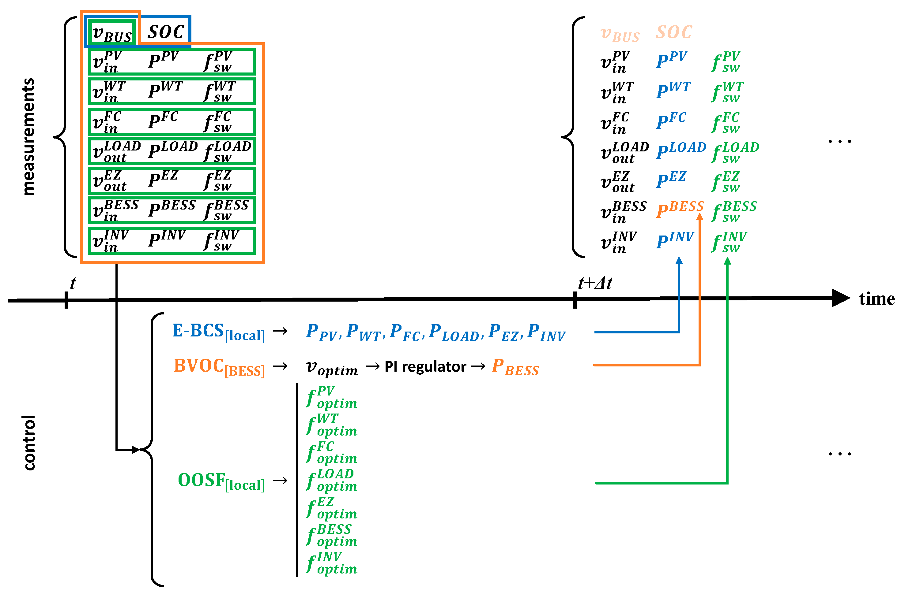
Figure 4 is a flow chart that shows how E-BCS, BVOCBESS and OOSF can be executed simultaneously. BVOCBESS and OOSF do not directly interfere with each other because they are independent. Nevertheless, they do interfere with each other indirectly. Indeed, BVOCBESS affects the values of the BESS power (), the SOC and , which will be measured in the next time step, and will affect then to the OOSF algorithm (see Equations (10) and (11)). And the other way round, OOSF produces changes in for every converter which, in its turn, will affect BVOCBESS when their measured values are fed to the EMS in the next time step (see Equation (7)).
6. Simulation Results
The MG operation has been simulated over seven days, in ten different scenarios S0 to S9. This section presents the results in three sub-sections. In the first sub-section, the quantitative results of efficiency improvement are provided for the ten scenarios considered. In the second sub-section, the dynamic response of the MG is graphically represented and explicated. Finally, in the third sub-section, the control parameters of BVOCBESS and OOSF are changed to evaluate how they affect the results.
6.1. Efficiency Increase
The global energy efficiency () is calculated to quantify the efficiency increase () achieved by each strategy with respect to the reference case (E-BCS). System (in green dotted line in Figure 5) is defined as that composed of the DC bus, the capacitors bank, and all the DC-DC converters.
This system is taken as a black box in which there are energy inputs and outputs. Global efficiency is defined in Equation (12) as the quotient of the energy coming out () divided by energy coming in ():
where represents the power injected/withdrawn to/from the system by the converter . The logical variables and are defined to distinguish when the BESS and the INV converters work as sources and when they work as loads (the superscript * indicates negation). The integration limits are zero (the beginning of the simulation), and (the end of the simulation = 7 × 24 = 168 h).
Ten simulations, corresponding to ten different scenarios, are performed. In the first simulation, S0, several elements have been simulated to fail in order to verify the robustness of the control system. The simulations S1 to S9, on the contrary, represent different scenarios of normal operation (i.e., no failures). In each simulation, different coefficients multiply the base RES generation and base LOAD consumption profiles. Table 2 summarizes the differences between the nine simulations S1 to S9:
For these ten simulations, base RES generation profile has been estimated based on meteorological data (solar irradiance, temperature and wind speed) from the Servei Meteorològic de Catalunya [25], and base LOAD profile corresponds to a residential electricity consumption profile. A time step of 100 ms is selected, coinciding with the refresh rate of both BVOCBESS and OOSF controllers. The switching frequency ranges are 20–100 kHz for IGBTs and 3–10 kHz for MOSFETs, as indicated previously in Equation (9). In each of the ten scenarios, the MG is simulated with four different control schemes:
- E-BCS
- E-BCS + BVOCBESS + OOSF
- E-BCS + BVOCBESS
- E-BCS + OOSF
BVOCBESS controls the BESS’ converter and OOSF is applied in all the MG’s converters. Global efficiency results obtained in the simulations are shown in Table 3:
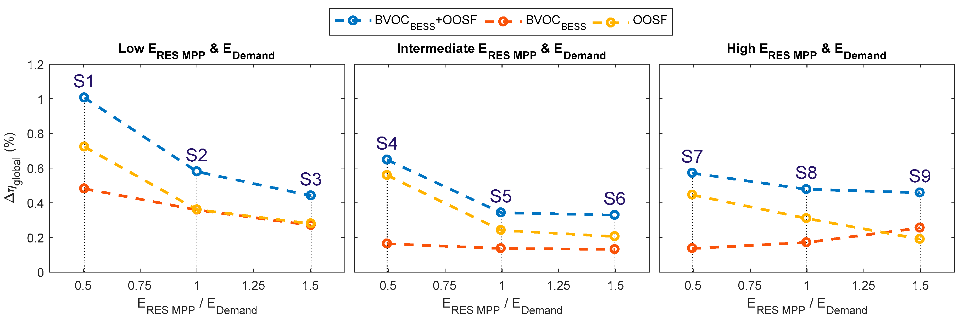
Each of the 40 simulations performed has taken an average of 15 min to complete, using MatlabR2017a–Simulink in Intel® Core™ i7-6700 CPU @ 4.40 GHz, 16 GB RAM. Figure 6 represents graphically the results of Table 3:
The results of the simulations reveal that simultaneously applying both BVOCBESS and OOSF strategies, result in a (blue in Figure 6) ranging from 0.329% in the worst scenario (S6) to 1.006% in the best case scenario (S1). Applying only BVOCBESS (orange) while switching the transistors at fixed frequencies (MOSFETs at 50 kHz and IGBTs at 4 kHz), the ranges from 0.131% (S6) to 0.481 (S1). And last, applying only OOSF (yellow), letting the bus voltage evolve according to VEC and SOCEC, the achieved ranges from 0.190% (S9) to 0.723% (S1).
These results are coherent with the efficiency curves information provided in Figure 3. There is a general tendency towards higher for lower powers, and vice versa, due to the characteristic shape of the efficiency curves. In the steep part of the curves (which corresponds to low power values), higher efficiency improvements are achievable, while for powers greater than maximum–efficiency power, efficiency optimization performance is limited due to the small differences existing in for different values of and .
Efficiency improvements accomplished by OOSF strategy do consistently show this effect in all the simulated scenarios: in all the cases, is higher for lower power flows. Hence, for a given RES profile, is higher for lower LOAD profiles. Indeed, the optimization performance of OOSF verifies (left graph of Figure 6). Similarly, for a given ratio , is higher for lower power flows: (first scenario of each of the three graphs in Figure 6).
On the other hand, BVOCBESS performance does not show this regularity as it highly depends on the specific combination of active converters performing the instantaneous power flows. For example, would be high in a moment when only WT and LOAD were active (WT directly feeding the LOAD) because the individual optimal bus voltage is 370 V for both converters, but would be much lower if the same power came from BESS instead of WT because individual optimal bus voltage is 250 V for the BESS converter and 370 V for the LOAD converter. The global optimal bus voltage in this last case would be the trade-off which minimizes the sum of power losses in both converters. This dependence on the particular MG’s power flows evolution is the cause for irregular results.
The efficiency improvements achieved with the two proposed optimization strategies, BVOSBESS and OOSF, are small but still interesting. Even though the MG’s efficiency increases range only from 0.3 to 1.0% (approx.), they are achieved by introducing changes in the discrete control algorithms of the DC-DC converters. Thus, they require (almost) no extra investment. Implementing both optimization strategies produces net energy (and economic) savings in all possible operating conditions. Nevertheless, BVOCBESS and OOSF optimization are best suited for microgrids applications which require low power flows compared to the nominal power of the converters and/or microgrids in which all the MG’s converters coincide in the same optimal bus voltage value .
Some application examples that meet these requirements can be Uninterruptible Power Supply (UPS) systems (in which the BESS operates at near zero power to maintain the battery floating), and remote Base Transceiver Stations (RBT) and weather stations, because their BESS are normally significantly oversized so that they can sustain the operation of the station for several days in case of generation shortage. In both cases, the BESS converter normally operates well below its nominal power and can benefit from OOSF high performance for low power. Furthermore, if the individual optimal bus voltage values of the MG’s converters coincide, BVOCBESS performance can be more significant than in the MG studied in this paper.
For other microgrids applications in which higher powers are involved and with a diversity of individual for different MG’s converters, BVOCBESS might be discarded in the sake of simplicity and robustness, considering that it is difficult to implement (it performs complex calculations and requires the utilization of an EMS that communicates with all the MG’s converters), and that is small for intermediate and high power flows.
6.2. Dynamic Response
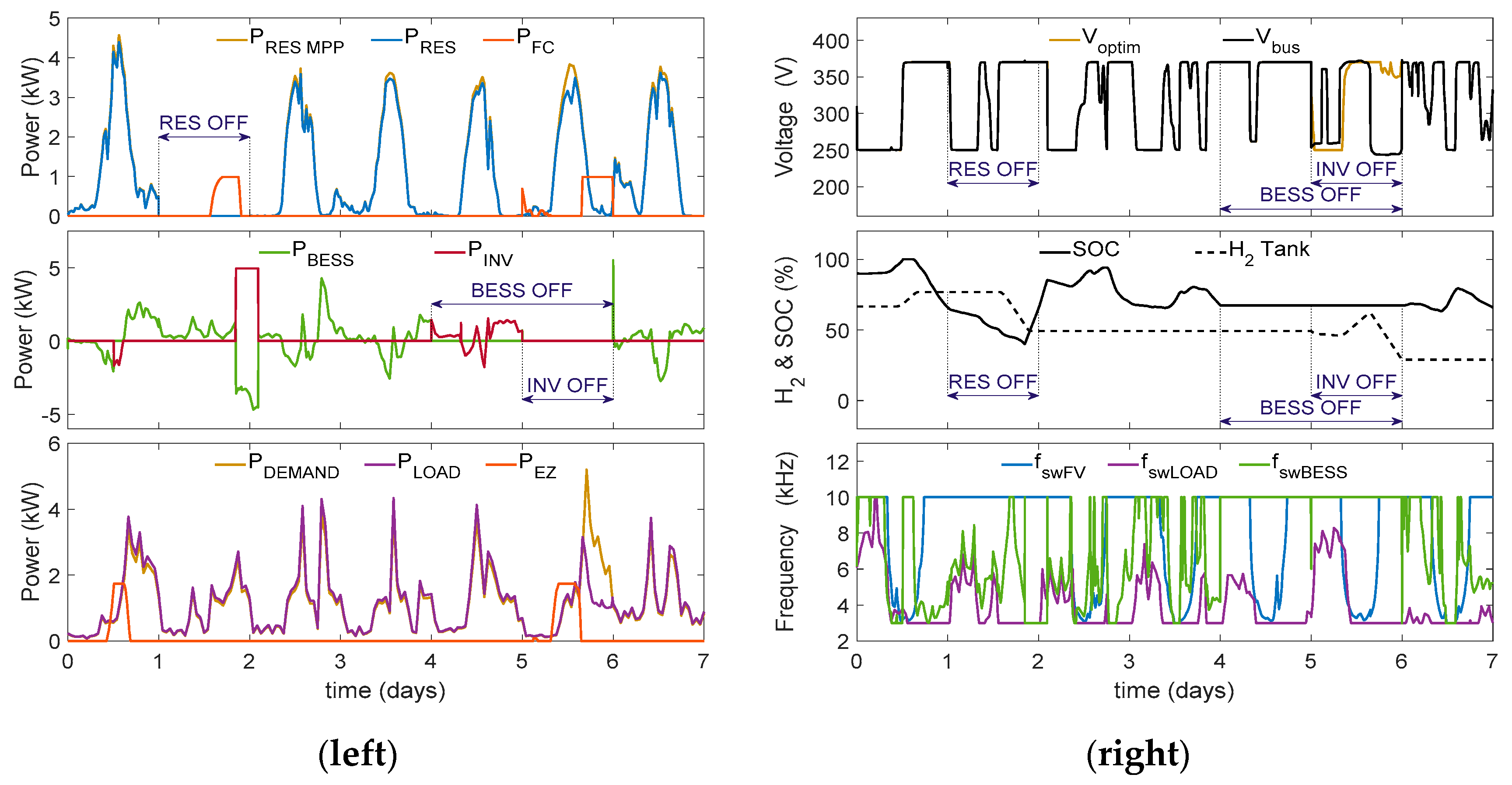
The simulation S0 is represented in Figure 7 and analyzed in this sub-section. The MG has been simulated implementing both BVOCBESS (in the BESS’ converter) and OOSF (in all the MG’s converters) simultaneously. In order to test MG’s robustness and verify that operation is sustained even in very adverse circumstances, several failures have been simulated:
- From to , all the renewable energy generation (PV and WT) is switched off.
- From to , the BESS is disconnected.
- From to , the INV is disconnected.
At the beginning of the first day, generation is higher than consumption and the surplus energy is used to charge the BESS until it reaches 100% SOC. EZ and INV are then activated. EZ leverages high generation to produce H2. INV injects the excess of RES generation power to the grid. During the evening, RES generation decreases and LOAD increases, so the BESS begins to discharge to provide power.
The second day, RES remain disconnected and the battery keeps feeding the LOAD. Battery SOC descends to low values, triggering the activation of FC and INV. First, FC delivers emergency power to the DC bus (consuming H2) and since SOC still keeps descending down to 40%, INV starts consuming full power from the grid to feed the loads and charge the battery up to 85%.
The third and fourth days, the BESS gets charged when RES power is greater than LOAD, and gets discharged when the opposite occurs. This is normal operation.
The fifth and sixth days, BESS remains disconnected. The control system permits to maintain MG stability, making the INV assume the power profile that would otherwise correspond to the BESS. The sixth day, INV (together with BESS) remains disconnected (this represents a BESS controller fault), leaving the MG not only operating in islanded mode, but also with no possibility of utilizing any bidirectional unit. Thus, generated power must constantly equal consumed power. VEC manages unidirectional units to balance the power being injected to and being consumed from the DC bus. The last day, the MG comes back to normal operation.
The system proves to be robust even in the face of severe failures. No undesired downtimes have occurred. The top right graph shows bus voltage evolution under BVOCBESS: the optimal voltage reference () is imposed, and BESS power is controlled such that bus voltage () follows that reference—except when both BESS and INV are down. The bottom right graph shows the result of OOSF: the switching frequencies constantly vary to match the optimal frequency of every converter. In all cases, the optimal switching frequency turns out to be high for low values of power, i.e., when core losses prevail.
6.3. Influence of Control Parameters in Optimization Performance
In this last sub-section, the parameters of BVOCBESS and OOSF are modified to evaluate how they affect the efficiency improvement achieved. The parameters studied are:
- : Refresh rate of BVOCBESS controller
- : Refresh rate of OOSF controllers
- Switching frequency optimization intervals
For this study, the operation of the MG has been simulated over a period of only 24 h because the simulation time step has been reduced from previous 100 ms to 10 ms. Executing the simulations over a seven days period would have required excessive computing resources and time. Each of the executed simulations (of 24 h of MG’s operation) has taken an average of 15 minutes to complete. The results are presented in Table 4:
Table 4 results indicate that BVOCBESS and OOSF performance can be slightly improved to some extent if the control parameters are chosen properly:
- : The refresh rate of BVOCBESS controller has very limited influence in overall BVOCBESS performance for the studied values. The capacitor’s bank smooths the bus voltage dynamic so it is slow compared to the evaluated . Calculating and updating the optimal bus voltage reference, , more frequently does not significantly improve the efficiency of BVOCBESS algorithm.
- Switching frequency ranges: If the range of possible switching frequencies is widened, efficiency improvements close to 0.3% can be obtained. However, it is important to mention that a new optimization problem arises here to select the most appropriate frequency limits. The trade-off between OOSF efficiency improvement, passive filters size and electromagnetic interferences restriction must be established.
- : The variations in OOSF performance are insignificant. Again, the power in all the MG’s units evolves very slowly compared to the evaluated .
Summarizing the results, the control parameters were already satisfactory. Changing the refresh rate of BVOCBESS and OOSF controllers produce nearly zero improvements. Only by widening the range of switching frequency window some appreciable efficiency increases might be obtained. Nevertheless, this has important drawbacks (e.g., increased current ripple) that might require re-designing the MG’s converters.
7. Conclusions
A self–managed DC MG has been described. Events-Based Control System (E-BCS), which is constituted of decentralized Voltage Event Control (VEC) and State of Charge Event Control (SOCEC), has been the starting point to evaluate two strategies to optimize the efficiency of the MG’s converters. E-BCS determines the power of each unit based on the bus voltage () and on the battery SOC. These laws prevent that and SOC reach extreme values by activating loads and deactivating sources when or SOC get too high, and deactivating loads and activating sources when or SOC get too low.
The two proposed optimization strategies have been explained and simulated. Both of them increase the efficiency of the MG’s DC-DC converters online, in any possible operation point. They utilize with two different approaches to minimize the power losses of the MG’s converters. The nonlinear optimization problems that they solve are formulated based on small–signal averaged deterministic loss models of the converters. The two strategies are independent from each other and can be implemented simultaneously. They are also compatible with economic optimization strategies.
Representative efficiency curves of two of the MG’s DC-DC converters at different switching frequencies and bus voltage values have been analyzed with the purpose of estimating the efficiency improvement that the optimization strategies can produce.
- Bus Voltage Optimization Control (BVOCBESS): The BESS power is controlled such that it fulfills two purposes: first, to balance the power of sources, loads and inverter and, second, to make the system work at the (varying) optimal bus voltage . The value of is calculated online as the minimizer of the sum of power losses in the MG’s DC-DC converters. Thus, this optimization applies to the whole set of converters, not to any particular individual converter.
- Online Optimization of Switching Frequency (OOSF): The gate drivers’ switching frequency of each DC-DC converter is optimized online to improve its energy efficiency.
MG operation has been simulated over seven days in ten different scenarios representing different electricity generation and consumption profiles. The resulting control system (E-BCS + BVOCBESS + OOSF) manages the MG in a stable manner and is capable of overcoming abnormal difficulties, such as the simultaneous failure of all the bidirectional units. The two optimization strategies result in low (yet interesting) efficiency improvements: = 0.329–1.006% (depending on the scenario considered); = 0.131–0.481%; = 0.190–0.723%.
Even though the efficiency improvements are low, they are based in discrete control algorithms so they require (almost) no extra investment. Best results occur when the MG’s sources/loads deliver/consume low powers.
Two main reasons explain the low results. First and foremost, the converter’s efficiency curves reveal small variations within the range of variation of and . Second, the optimal bus voltage is different for individual converters causing the BVOCBESS algorithm to calculate the as the trade–off that minimizes the overall power losses.
BVOCBESS and OOSF optimization strategies are appropriate for microgrids applications which require low power flows compared to the nominal power of the converters and/or microgrids in which all the MG’s converters coincide in a single optimal bus voltage value . Possible application examples that meet these requirements include Uninterruptible Power Supply (UPS) systems and remote Base Transceiver Stations (RBT) and weather stations.
Author Contributions
Conceptualization, D.G.E., H.V.B., À.C.P. and L.M.S.; Data curation, D.G.E.; Formal analysis, D.G.E.; Funding acquisition, H.V.B. and À.C.P.; Investigation, D.G.E.; Methodology, D.G.E.; Project administration, H.V.B. and À.C.P.; Resources, H.V.B., À.C.P. and L.M.S.; Software, D.G.E.; Supervision, L.M.S.; Visualization, D.G.E.; Writing—original draft, D.G.E.; Writing—review & editing, D.G.E., H.V.B. and À.C.P.
Funding
This research was funded by the Spanish Ministry of Economy and Competitiveness under grants BES-2016-077460, DPI2015-67292-R and DPI2017-84572-C2-1-R.
Conflicts of Interest
The authors declare no conflict of interest.
Appendix A
This Appendix contains the complete system of equations describing the operation of the converters and their energy efficiency. Equations (A1)–(A37) are utilized to model the DC-DC converters in the simulation of the MG operation.
Equations (A1)–(A37) are also used to solve the BVOCBESS optimization problem considered in Equation (3) (substituting the physical magnitude by the calculation variable ) and the OOSF optimization problems considered in Equation (9) (substituting the physical magnitude by the calculation variable ).
Only the variables and parameters appearing here for the first time will be described.
Appendix A.1. General Equations
The following equations apply to all the DC-DC converters present in the MG:
where is the voltage across the inductor during the ON time of the duty cycle, is the number of turns, is the cross-sectional area of the inductor’s core.
Appendix A.2. General Parameters
The following parameters apply to all the DC-DC converters present in the MG:
Appendix A.3. Converters Models: Parameters

Table A1.
Converters parameters.
| Device | PV | WT | FC | LOAD | EZ | BESS | INV | |||||||
|---|---|---|---|---|---|---|---|---|---|---|---|---|---|---|
| Inductors | ||||||||||||||
| - | - | - | - | |||||||||||
| Transistors | ||||||||||||||
| - | - | - | - | - | ||||||||||
| Diodes | - | - | ||||||||||||
| - | - | |||||||||||||
| P.S. | ||||||||||||||
P.S. stands for power supply of the driver, and (fsw) is the fixed frequency value when E-BCS only, or E-BCS + BVOC, are utilized.
Appendix A.4. Converter Models: Equations
The following equations are employed in the simulation to model the DC-DC converters operation. They are executed iteratively until the efficiency error is less than 0.1%. These equations are also utilized to formulate the optimization problems of BVOCBESS (substituting the physical magnitude by the calculation variable ) and OOSF (substituting the physical magnitude by the calculation variable ):
Table A2.
Equations utilized to model the converters’ power losses.
| PV converter (Boost) [IGBT] | (A8) | ||
| (A9) | |||
| (A10) | |||
| WT converter (Boost) [MOSFET] | (A11) | ||
| (A12) | |||
| (A13) | |||
| FC converter (Quad. boost) [MOSFET] | (A14) | ||
| (A15) | |||
| (A16) | |||
| (A17) | |||
| LOAD converter (Quad. buck) [IGBT] | (A18) | ||
| (A19) | |||
| (A20) | |||
| (A21) | |||
| EZ converter (Quad. buck) [MOSFET] | (A22) | ||
| (A23) | |||
| (A24) | |||
| (A25) | |||
| BESS converter (Bidirec-tional) [IGBT] | Boost mode. in = battery out = MG’s bus | (A26) | |
| (A27) | |||
| (A28) | |||
| Buck mode. in = MG’s bus out = battery | (A29) | ||
| (A30) | |||
| (A31) | |||
| INV converter (Bidirec-tional) [IGBT] | Boost mode. in = MG’s bus out = inv DC | . | (A32) |
| . | (A33) | ||
| (A34) | |||
| Buck mode. in = inv DC out = MG’s bus | (A35) | ||
| (A36) | |||
| (A37) | |||
Where is the volume of the inductor’s core.
References
- Hirsch, A.; Parag, Y.; Guerrero, J. Microgrids: A review of technologies, key drivers, and outstanding issues. Renew. Sustain. Energy Rev. 2018, 90, 402–411. [Google Scholar] [CrossRef]
- Dragicevic, T.; Lu, X.; Vasquez, J.C.; Guerrero, J.M. DC Microgrids–Part I: A Review of Control Strategies and Stabilization Techniques. IEEE Trans. Power Electron. 2016, 31, 4876–4891. [Google Scholar] [CrossRef]
- Zhao, J.; Dörfler, F. Distributed control and optimization in DC microgrids. Automatica 2015, 61, 18–26. [Google Scholar] [CrossRef]
- Guerrero, J.M.; Vasquez, J.C.; Matas, J.; De Vicuña, L.G.; Castilla, M. Hierarchical control of droop-controlled AC and DC microgrids—A general approach toward standardization. IEEE Trans. Ind. Electron. 2011, 58, 158–172. [Google Scholar] [CrossRef]
- Nguyen, D.T.; Le, L.B. Optimal energy trading for building microgrid with electric vehicles and renewable energy resources. In Proceedings of the ISGT 2014, Washington, DC, USA, 19–22 February 2014; pp. 1–5. [Google Scholar]
- Li, C.; de Bosio, F.; Chaudhary, S.K.; Graells, M.; Vasquez, J.C.; Guerrero, J.M. Operation cost minimization of droop-controlled DC microgrids based on real-time pricing and optimal power flow. In Proceedings of the IECON 2015–41st Annual Conference of the IEEE Industrial Electronics Society, Yokohama, Japan, 9–12 November 2015. [Google Scholar]
- Lujano-Rojas, J.M.; Dufo-Lopez, R.; Bernal-Agustin, J.L.; Catalao, J.P.S. Optimizing Daily Operation of Battery Energy Storage Systems Under Real-Time Pricing Schemes. IEEE Trans. Smart Grid 2017, 8, 316–330. [Google Scholar] [CrossRef]
- Wang, Y.; Huang, Y.; Wang, Y.; Li, F.; Zhang, Y.; Tian, C. Operation Optimization in a Smart Micro-Grid in the Presence of Distributed Generation and Demand Response. Sustainability 2018, 10, 847. [Google Scholar] [CrossRef]
- Gonzalez-Garrido, A.; Saez-de-Ibarra, A.; Gaztanaga, H.; Milo, A.; Eguia, P. Annual Optimized Bidding and Operation Strategy in Energy and Secondary Reserve Markets for Solar Plants with Storage Systems. IEEE Trans. Power Syst. 2018, 8950, 1–10. [Google Scholar] [CrossRef]
- Anand, S.; Fernandes, B.G. Optimal voltage level for DC microgrids. In Proceedings of the IECON 2010–36th Annual Conference on IEEE Industrial Electronics Society, Glendale, AZ, USA, 7–10 November 2010; pp. 3034–3039. [Google Scholar] [CrossRef]
- Zhao, Z.; Hu, J.; Chen, H. Bus Voltage Control Strategy for Low Voltage DC Microgrid Based on AC Power Grid and Battery. In Proceedings of the 2017 IEEE International Conference on Energy Internet (ICEI), Beijing, China, 17–21 April 2017; pp. 349–354. [Google Scholar] [CrossRef]
- Dahiya, R. Voltage regulation and enhance load sharing in DC microgrid based on Particle Swarm Optimization in marine applications. Indian J. Geo-Mar. Sci. 2017, 46, 2105–2113. [Google Scholar]
- Liu, J.M.; Yu, C.J.; Kuo, Y.C.; Kuo, T.H. Optimizing the efficiency of DC-DC converters with an analog variable-frequency controller. In Proceedings of the APCCAS 2008–2008 IEEE Asia Pacific Conference on Circuits and Systems, Macao, China, 30 November–3 December 2008; pp. 910–913. [Google Scholar] [CrossRef]
- Sizikov, G.; Kolodny, A.; Fridman, E.G.; Zelikson, M. Frequency dependent efficiency model of on-chip DC-DC buck converters. In Proceedings of the 2010 IEEE 26-th Convention of Electrical and Electronics Engineers in Israel, Eliat, Israel, 17–20 November 2010; pp. 651–654. [Google Scholar] [CrossRef]
- Jauch, F.; Biela, J. Generalized modeling and optimization of a bidirectional dual active bridge DC-DC converter including frequency variation. In Proceedings of the 2014 International Power Electronics Conference (IPEC-Hiroshima 2014–ECCE ASIA), Hiroshima, Japan, 18–21 May 2014; pp. 1788–1795. [Google Scholar] [CrossRef]
- Çelebi, M. Efficiency optimization of a conventional boost DC/DC converter. Electr. Eng. 2018, 100, 803–809. [Google Scholar] [CrossRef]
- Al-Hoor, W.; Abu-Qahouq, J.A.; Huang, L.; Batarseh, I. Adaptive variable switching frequency digital controller algorithm to optimize efficiency. In Proceedings of the 2007 IEEE International Symposium on Circuits and Systems, New Orleans, LA, USA, 27–30 May 2007; pp. 781–784. [Google Scholar]
- Liu, J.-M.; Wang, P.-Y.; Kuo, T.-H. A Current-mode DC–DC buck converter with efficiency-optimized frequency control and reconfigurable compensation. IEEE Trans. Power Electron. 2012, 27, 869–880. [Google Scholar] [CrossRef]
- Zhao, L.; Li, H.; Liu, Y.; Li, Z. High efficiency variable-frequency full-bridge converter with a load adaptive control method based on the loss model. Energies 2015, 8, 2647–2673. [Google Scholar] [CrossRef]
- MATLAB R2017a and Simulink; The MathWorks, Inc.: Natick, MA, USA, 2017.
- Bosque-Moncusi, J.M. Ampliación, Mejora e Integración en la Red de un Sistema Fotovoltaico. Ph.D. Thesis, Universitat Rovira i Virgili, Tarragona, Spain, 2015. [Google Scholar]
- Eichhorn, T. Boost Converter Efficiency through Accurate Calculations. Power Electron. Technol. Mag. Online 2008, 9, 30–35. [Google Scholar]
- Stasi, F. De Working with Boost Converters; Texas Instruments Incorporated: Dallas, TX, USA, 2015; pp. 1–11. [Google Scholar]
- Hurley, W.G.; Wölfle, W.H. Transformers and Inductors for Power Electronics Transformers and Electronics; Wiley: Hoboken, NJ, USA, 2013; Volume 8, ISBN 9780071594325. [Google Scholar]
- Servei Meteorològic de Catalunya. Available online: http://www.meteo.cat/wpweb/climatologia/serveis-i-dades-climatiques/series-climatiques-historiques/ (accessed on 15 June 2018).
Figure 1.
MG architecture. The MG is composed of a DC bus in which the following elements are connected: two Renewable Energy Sources (RES) (PV and WT), a controllable source (FC), a capacitors bank, a bidirectional grid-inverter (INV), a battery system (BESS), critical loads (LOAD), and a controllable load (EZ).

Figure 2.
E-BCS control laws: VEC in the graph above and SOCEC in the graph below.

Figure 3.
Efficiency curves of LOAD’s and BESS’ converters at different switching frequencies (I) and bus voltages (II): (a) Quadratic buck converter interfacing with LOAD; (b) Bidirectional converter interfacing with BESS.
Figure 3.
Efficiency curves of LOAD’s and BESS’ converters at different switching frequencies (I) and bus voltages (II): (a) Quadratic buck converter interfacing with LOAD; (b) Bidirectional converter interfacing with BESS.

Figure 4.
MG management flow chart describing the process of simultaneous E-BCS (in blue), BVOCBESS (in orange) and OOSF (in green). Each time step, say in time , the E-BCS local controller of each converter receives the measured value of and SOC and, from them, determines the correspondent . The BVOCBESS centralized controller (i.e., the BESS controller) receives all the MG’s measured values and, from them, calculates ; a PI regulator determines then from this reference. The OOSF local controller of each converter receives the measured value of , (note that one of these two is invariably equal to . for all converters ), , and and, from them, calculates the optimal . The calculated values and by the three algorithms are then imposed and, thus, they will coincide with the measured values in the next time step . Measured and SOC appear in light orange in . because, although they are not directly determined by BVOCBESS, they are highly influenced by .

Figure 5.
Possible power flows in the MG. The green rectangle defines the system

Figure 6.
Energy efficiency improvement achieved by simultaneous BVOCBESS + OOSF optimization strategies, only BVOCBESS, and only OOSF in different scenarios.
Figure 6.
Energy efficiency improvement achieved by simultaneous BVOCBESS + OOSF optimization strategies, only BVOCBESS, and only OOSF in different scenarios.

Figure 7.
MG simulation over 7 days with the optimized control system: E-BCS + BVOCBESS + OOSF. From top to bottom, the graphs in the left column represent: (1) Sources power: available RES power, actual RES power injected in the DC bus, and FC power injected in the DC bus; (2) BESS and INV power; (3) Loads power: critical loads electricity demand, actual LOAD power consumed from the DC bus, and EZ power consumed from the DC bus. The graphs in the right column represent: (1) Optimum bus voltage reference and actual bus voltage evolution; (2) SOC and hydrogen tank level evolution; (3) Optimized switching frequencies of three converters: PV, LOAD and BESS.

Table 1.
MG’s elements.
| Sources | PV: Photovoltaic Field | WT: Wind Turbine | FC: Fuel Cell |
| Loads | LOAD: Residential profile DC load | EZ: Electrolyzer | |
| Bidirectional Units | BESS: Battery Energy Storage System | INV: Bidirectional inverter | |
Table 2.
Characteristics of the ten simulation scenarios.
| RES & LOAD Energies | Failures Simulation | Low Energy | Intermediate Energy | High Energy | ||||||
|---|---|---|---|---|---|---|---|---|---|---|
| S0 | S1 | S2 | S3 | S4 | S5 | S6 | S7 | S8 | S9 | |
| (kWh) | 161.2 | 37.7 | 113.1 | 188.5 | ||||||
| 1.20 | 0.75 | 1.00 | 1.33 | 0.75 | 1.00 | 1.33 | 0.75 | 1.00 | 1.33 | |
Table 3.
MG global efficiency improvement under four different control strategies, in ten different scenarios S0–S9, over seven days operation.
Table 3.
MG global efficiency improvement under four different control strategies, in ten different scenarios S0–S9, over seven days operation.
| Control Strategy | Failures Simulation | No Failures Simulation | ||||||||
|---|---|---|---|---|---|---|---|---|---|---|
| Low Energy | Intermediate Energy | High Energy | ||||||||
| S0 | S1 ELOAD < ERES | S2 ELOAD = ERES | S3 ELOAD > ERES | S4 ELOAD < ERES | S5 ELOAD = ERES | S6 ELOAD > ERES | S7 ELOAD < ERES | S8 ELOAD = ERES | S9 ELOAD > ERES | |
| Control | η: Efficiency | |||||||||
| E-CBS (reference) | 86.184% | 77.948% | 79.504% | 80.841% | 86.126% | 86.990% | 87.295% | 87.250% | 87.140% | 87.339% |
| Optimization | Δη: Efficiency improvement over reference E-CBS | |||||||||
| BVOCBESS + OOSF | 0.608% | 1.006% | 0.580% | 0.441% | 0.648% | 0.343% | 0.329% | 0.571% | 0.4776% | 0.458% |
| BVOCBESS | 0.146% | 0.481% | 0.359% | 0.270% | 0.164% | 0.136% | 0.131% | 0.137% | 0.1707% | 0.255% |
| OOSF | 0.444% | 0.723% | 0.360% | 0.280% | 0.559% | 0.241% | 0.205% | 0.446% | 0.3100% | 0.190% |
S0 represents the operation of the MG scheduling failures in RES, BESS and INV. This permits to verify that the optimized control system responds correctly to failures and rapid changes. S0 is analyzed in the next sub-section. S1, S2 and S3 represent the MG operation when the power of all the elements is low (compared to their nominal power). These three simulations correspond to increasing ratios : 0.75, 1.00 and 1.33. This ratios scheme is repeated for intermediate (S4–S6) and high powers (S7–S9).
Table 4.
Influence of control parameters on optimization performance.
| Control Strategy | Reference Case Scenario S0 | Modified Control Parameters | ||||
| Faster BVOC | Slower BVOC | Wider FSW Range | Faster OOSF | Slower OOSF | ||
10 ms | 5 s | 10–200 kHz | 5 s | |||
| E-BCS | η: Efficiency = 85.969% | |||||
| Optimization | Δη: Efficiency improvement over E-BCS | Δη: Efficiency improvement over reference case | ||||
| BVOCBESS + OOSF | 1.029% | 3.8 × 10⁻⁴% | −0.009% | 0.293% | 1 × 10⁻⁶% | −4 × 10⁻⁶% |
| BVOCBESS | 0.216% | 0.001% | −0.014% | - | - | - |
| OOSF | 0.768% | - | - | 0.265% | 1 × 10⁻⁶% | –3 × 10⁻⁶% |
© 2018 by the authors. Licensee MDPI, Basel, Switzerland. This article is an open access article distributed under the terms and conditions of the Creative Commons Attribution (CC BY) license (http://creativecommons.org/licenses/by/4.0/).
Share and Cite
MDPI and ACS Style
García Elvira, D.; Valderrama Blaví, H.; Cid Pastor, À.; Martínez Salamero, L. Efficiency Optimization of a Variable Bus Voltage DC Microgrid. Energies 2018, 11, 3090. https://doi.org/10.3390/en11113090
AMA Style
García Elvira D, Valderrama Blaví H, Cid Pastor À, Martínez Salamero L. Efficiency Optimization of a Variable Bus Voltage DC Microgrid. Energies. 2018; 11(11):3090. https://doi.org/10.3390/en11113090
Chicago/Turabian StyleGarcía Elvira, David, Hugo Valderrama Blaví, Àngel Cid Pastor, and Luis Martínez Salamero. 2018. "Efficiency Optimization of a Variable Bus Voltage DC Microgrid" Energies 11, no. 11: 3090. https://doi.org/10.3390/en11113090
Note that from the first issue of 2016, this journal uses article numbers instead of page numbers. See further details here.