An Improved Modulation Strategy Combining Phase Shifted PWM and Phase Disposition PWM for Cascaded H-Bridge Inverters


College of Electrical and Information Engineering, Hunan University, Changsha 410082, China
*
Author to whom correspondence should be addressed.
Energies 2017, 10(9), 1327; https://doi.org/10.3390/en10091327
Submission received: 10 July 2017
/
Revised: 23 August 2017
/
Accepted: 30 August 2017
/
Published: 2 September 2017
(This article belongs to the Special Issue Advanced Control Techniques for Power Converters)
Abstract
:Multilevel modulation strategy is an important factor affecting the output performance of multilevel converters. In this paper, the relationship between phase-shifted pulse width modulation (PWM) and phase disposition PWM is analyzed, and then an improved hybrid modulation strategy is proposed for cascaded H-bridge. In addition, the implementation method of multilevel discontinuous modulation for an improved modulation strategy is described. The new modulation strategy is optimized to increase the DC link voltage utilization and further improvement in output harmonics by the injection of a common voltage into the reference. Simulation and experiment verify the effectiveness of the proposed modulation strategy.
1. Introduction
Cascaded H-bridge (CHB) inverters, as one kind of existing commercial topologies of multilevel voltage-source inverters, have received a lot of attention in recent years. The obvious advantages are easily realized higher power, more outstanding harmonics performance, and modularity [1,2]. Many efforts have been made to adapt the original modulation techniques applied to the two-level converter for multilevel inverters [3,4]. Two well-known modulation techniques, phase-shifted PWM (PS-PWM) and phase disposition PWM (PD-PWM), are referred in this paper.
The phase-shifted PWM is the standard modulation strategy for cascaded multilevel inverters due to the fact that it can yield a good result in reducing output harmonics and maintaining a power distribution balance among power cells [5,6]. Researchers analyzed the generalized theory of PS-PWM, which obtains the law of full-range phase-shift angle on harmonic minimization for a cascaded H-bridge [7]. Considered the operation condition, an adaptive modulation method in [8] is proposed to improve the operating characteristics under unbalanced conditions. The phase shift angle of the method is changed with the operating conditions. Currently, another research hotspot is based on the carrier phase shift of the capacitor voltage control, by implementing a balanced control algorithm in each carrier cycle to achieve voltage balance [9].
Phase disposition PWM is superior to phase-shifted PWM modulation strategies in getting the lowest harmonic distortion for line voltage, but performs poorly for balancing the power distribution among the cells, which makes it unsuitable for CHB inverters. Much work has been done to modify the phase disposition PWM for CHB inverters to achieve an improved output voltage. In [6], the author offered an equivalent PD-PWM for cascaded inverters. But this strategy can work under discontinuous modulation and a general strategy for balancing the power distribution among the cells is not presented either. Mauricio Angelo proposed a method that applies the PD-PWM to a five-level CHB inverter successfully in [10]. However, the extension of the method to a higher number of levels is not addressed. In [11], a method is presented to achieve an equivalent PD-PWM for CHB inverters. However, the author ignored the actual working situation of power semiconductors in practice and did not point out the constraint condition needed to be noticed when the strategy is applied to a three-phase system. In [12], a sorting algorithm is proposed to obtain better disposition of gates signals and distribution of switch losses when compared with traditional PD modulation, but is lacking in relevant experimental support.
Some researchers have studied the loss and dissipation of the two modulation methods. The power loss and thermal model of the power device in several different modulation strategies [13] are analyzed for the half bridge, providing a reference for the full bridge of this paper, which is mainly from the perspective of total harmonic distortion analysis.
A new modulation strategy combining the advantages of PS-PWM and PD-PWM for three-phase CHB inverters is introduced in this paper. The new modulation strategy not only solves the power distribution unbalancing problem in PD-PWM in virtue of features of PS-PWM but maintains the excellent performance in reducing output harmonics in PD-PWM. The new modulation strategy is optimized to increase the DC link voltage utilization and further improvement in output harmonics by the injection of a common voltage into the reference. A concise and effective multilevel discontinuous modulation strategy based on the new modulation strategy for N-level CHB inverters is also proposed to decrease the switch times and reduce the switching loss. Simulation and experimental results are given to prove the effectiveness of the new modulation strategy and discontinuous modulation strategy.
2. Principle of the Proposed Strategy
The object of the new strategy is to attain a similar output performance achieved by phase disposition PWM and to take the advantage of phase-shifted PWM in effective utilizing switching frequency and balancing the power distribution among cells.
2.1. New Strategy for Single Phase System
A concept of the equivalent carrier is introduced to derive the relationship between both modulation strategies in an intuitive way and the method proposed in [11] is simplified and refined to be more suitable for the practical system.
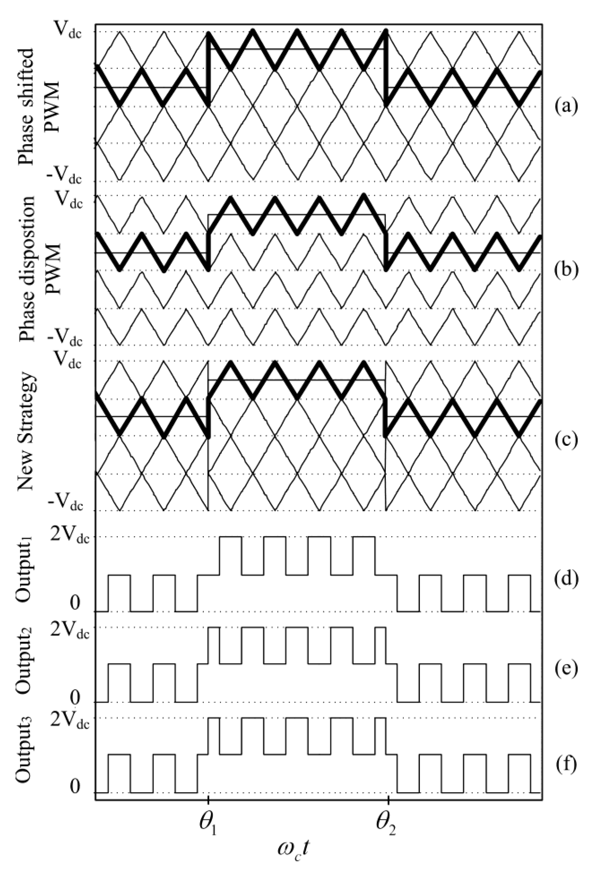
Figure 1a,b illustrates PS-PWM and PD-PWM strategies with an identical reference for a five-level CHB converter, which consists of two H-bridge power cells. In both modulation strategies, four triangular carriers are necessary on account of the number of switch bridges to be driven [10]. The average frequency or the total number of switch transitions is same for both strategies.
These two group carriers are subdivided into four intervals equally in the vertical direction by the dotted lines (boundary lines). The boundary lines subdivide the long line segments of carriers to short line segments. When just focusing on short line segments (the black bold lines shown in Figure 1a–c) in the interval where the reference belongs and regard these line segments as integrity, we obtain the equivalent carrier. It can be seen from the Figure 1a–c that the equivalent carrier can be considered as a series of triangle waves distributed in the different interval with the same frequency and the same amplitude.
The equivalent carrier is a simplification of the original real carriers and consists of the triangle waves intersecting the reference in each interval. The introduction of equivalent carrier provides an intuitive method to analyze the relationship between the reference and the total output voltage. It can be seen from the figure that the time when the output waveforms change is just consistent with the time when the reference crosses the equivalent carrier. Additionally, it is a good choice to use the equivalent carrier to identify the similarities and differences in total output voltages between different modulation strategies because the equivalent carrier only cares about the total output voltage without focusing on the output of each power cell. Figure 1a,b show that the equivalent carriers for both modulation strategies have the same frequency and the same peak-to-peak amplitude, but differ only in phase from θ1 to θ2. It is clearly shown that the output voltages for both strategies also differ only from θ1 to θ2 in Figure 1d,e.
The characteristics of both modulation strategies attribute to the difference between these two equivalent carriers. There will be a sudden 180° phase change of PDS PWM’s equivalent carrier when the reference transits to another interval because of the similarity between the phase shifted and alternative phase opposition disposition (APOD) where carriers in the adjacent interval are in opposition [14,15]. On the contrary, the equivalent carrier of PD-PWM keeps its continuity in phase and no sudden phase change will occur due to the fact that the carriers in each interval are in phase.
There is no question that with the help of periodicity of the equivalent carrier, an appropriate phase shift of PS-PWM’s carriers (in fact, the equivalent carrier is also shifted), at the time the reference crosses the boundary from one interval to another, can eliminate the phase discontinuity of PS-PWM’s equivalent carrier and achieve the same output waveforms with the phase disposition PWM strategy.
Figure 1c shows the operating characteristic of the proposed strategy. The positive 45° phase shift of the carriers occurs at θ1 and θ2. It is easy to find that after the adjustment of carriers, the proposed strategy and phase disposition PWM possess the same equivalent carrier and the same output waveforms.
In fact, this operation can be extended to an arbitrary N-level CHB inverter for an equivalent PD-PWM where the main feature of carriers for PS-PWM still remains. General rules are offered for getting the carriers of the new modulation strategy.
- (1)
- Divide all the carriers of PS-PWM to N − 1 intervals of the same width in the vertical direction.
- (2)
- Every time when the reference crosses the boundary from one interval to the adjacent one, we adopted a positive phase shift of the carriers that have been generated already. The amount of phase in terms of the carrier’s period is given by:
The factor 1/(N − 1) represents the frequency of the equivalent carrier N − 1 times of the real carries. In addition, the situation that the reference crosses over several boundary lines at the same time is not considered here because high dv/dt in the output voltage should be avoided in practice. The reference should be limited to only transit to the adjacent interval in one equivalent carrier cycle.
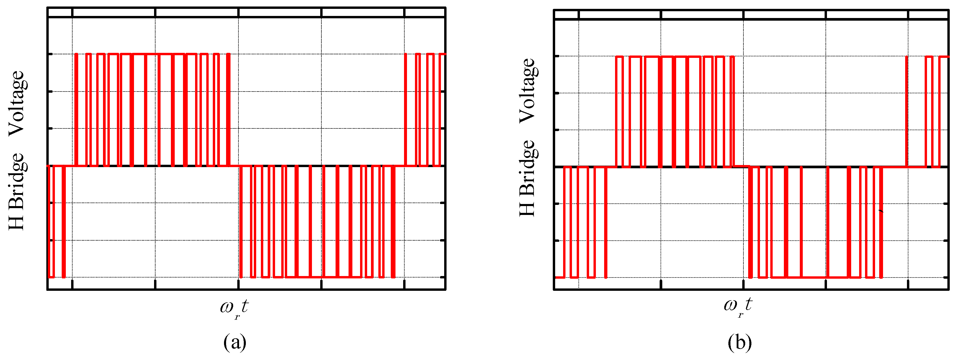
It should be mentioned that although in theory a negative phase shift of the carriers is also capable of achieving desired results which are proposed in [11], it can cause extra switching transitions of the power semiconductor in a cycle of carriers (roughly illustrated in Figure 2a,b) and is therefore not recommended in practice.
At this point we have obtained the new modulation strategy for single phase system.
2.2. New Strategy for Three-Phase System
Since substantial harmonic energy is put into the first carrier component in each phase voltage and cancels in the line voltage, the PD-PWM achieves a better output line voltage than that of phase-shifted PWM [6,15]. In the same way, the achievement of the desired results for the new strategy relies on the effective cancellation of first carrier harmonics in line voltage.
For a three-phase system, three different groups of carriers are indispensable because each reference of three phases always does not transit to another interval at the same time. Although the phase of one certain equivalent carrier has been decided, the phase difference between each equivalent carrier has not been decided yet. Thus, the question of how to decide and adjust a phase difference between each equivalent carrier becomes a new problem which does not occur in the PD-PWM, where three phase references are compared with a common group of carriers.
Simulation results show that the cancellation of first carrier harmonics in each phase voltage requires equivalent carriers of each phase to be in phase. On the other hand, the possible different initial position of each reference produces a phase difference of equivalent carrier between each phase, which is a contrast to PD-PWM where all the equivalent carriers of each phase are in phase naturally because three phase references are compared with a common group of carriers.
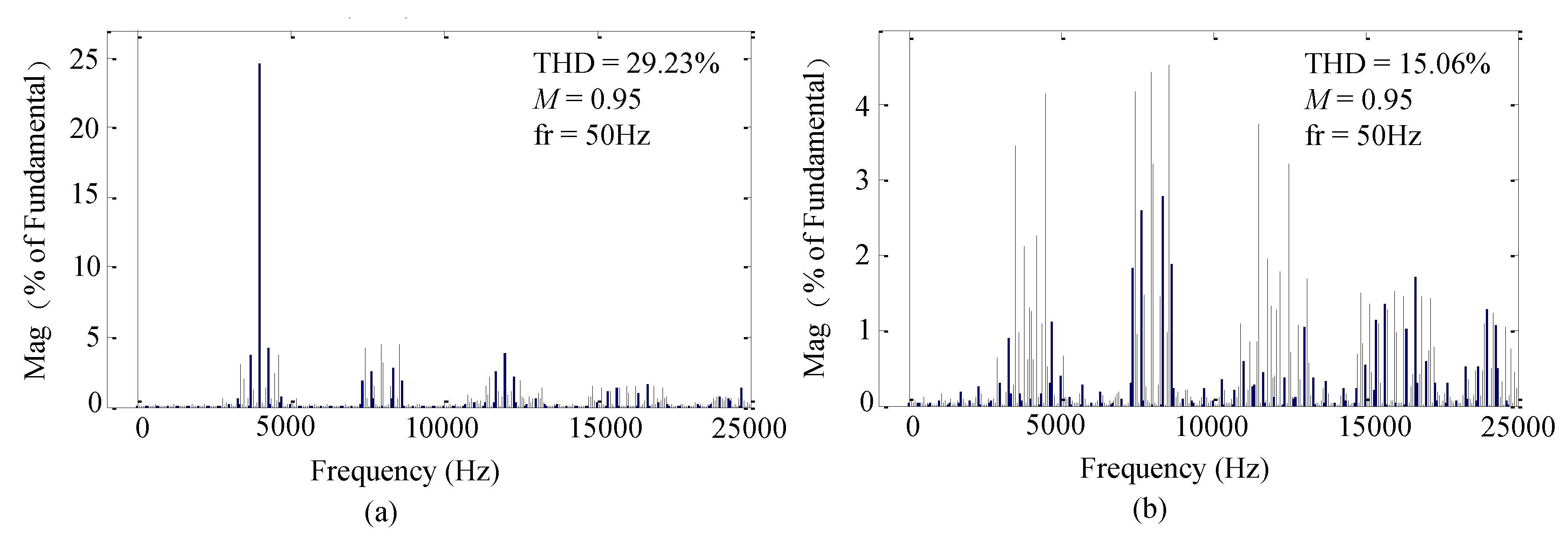
Figure 3 shows phase deviation of equivalent carriers caused by the different initial position of references. The reference for phase A starts from the interval just above zero value reference, whereas the reference for phase B starts from the interval just below zero value reference. Because of the different initial position of references, the equivalent carriers for phase A and B turn out to be opposite in phase.
Figure 4a shows the harmonics profile of line voltage where the equivalent carriers for phase A and B are just opposite in phase. Figure 4b shows the harmonics profile of line voltage where the equivalent carriers for phase A and B are in phase. Both harmonics profiles are obtained with 1 kHz switching frequency, 50 Hz frequency reference frequency; the modulation depth is M = 0.95. For the modulation depth M = Vdc/Vrp, Vdc is the DC voltage of the power cells and Vrp is the peak value of the reference. It is obvious that first carrier harmonics do not cancel in line voltage sufficiently because of the phase deviation.
Hence, it is necessary to take a measure to meet the constraint condition that the equivalent carriers of each phase should be in phase. Two ways are offered as follow:
- (1)
- Make three-phase references start from the same value at the beginning. For example, start from zero.
- (2)
- Take one phase’s equivalent carrier as a standard and properly shift the other two phases carriers at the beginning to make their equivalent carriers’ phase consistent with the standard.
A fundamental framework of the new strategy for the three-phase system has been established so far. Generally, a zero-sequence voltage is added to the three-phase references to improve DC link voltage utilization [16,17], as shown below.
It is preferable that only when the modulation depth M is more than 1, the offset voltage is injected into each phase reference to avoid introducing extra common voltage into the output phase voltage. It means that is zero when depth M is under 1.
In [18], a further adjustment of the phase reference is made to obtain an improved performance in output voltage. The author vertically shifts the reference voltages to a common carrier band and then centers the active space vectors in the switching cycle by adjusting the positions of the first and last switching transitions to optimize the harmonic profile. The new reference and the common voltage that centers the active space vectors can be described mathematically as:
Finally, we obtain the optimized new strategy by adding and to the reference waveform , or .
2.3. Discontinuous Modulation Based on New Strategy
Figure 5 shows the common carrier and the new references , and . Apparently, the easiest strategy for discontinuous modulation of multilevel inverter for PD-PWM could be achieved by eliminating the first or the last crossing (namely the first state or the last state in the space vector) with an adjustment of the new references with the offset voltage of:
or
Similarly, the final reference voltages for discontinuous modulation can be calculated by summing the two common voltages to or .
However, this is not the case for the new strategy to obtain discontinuous modulation yet, considering that the new strategy is only equal to the PD-PWM in the output voltage. Clearly, the final reference to phase in which pulse is arranged to be eliminated, still crosses downwards or upwards with the real carriers, although it does not cross the equivalent carrier. Due to the intersections of the carriers and the reference, the switching transitions still exist.
In order to avoid the switching transitions, the carriers of the arranged phase should be kept unchanged in the switching cycle. Then the reference no longer crosses downwards or upwards with the carriers, and therefore no switching transition is generated. The detailed operation of this strategy will be shown later in the Section 3.1.
Another thing to be noted is that the efficiency to reduce the switching frequency by eliminating the first state in each switching sequence is much lower than that by eliminating the last state in practice. To eliminate the last state, we simply maintain the status that produced in the former cycle of the equivalent carrier and no switching transition is needed. However, to eliminate the first state, the output waveforms must step one level up and thus a switching transition will be introduced. Correspondingly, another switching transition is necessary to make the output waveforms step one level down when the corresponding reference do not cross the common carrier firstly. Moreover, in the multilevel application the state being the first crossing or the last crossing the common carrier rapidly rotates among three phases after the phase references are adjusted to a common carrier band, and therefore extra switching transition resulted from eliminating the first state will sharply degenerate its ability to reduce the switching frequency.
3. Simulation and Experimental Results
3.1. Simulation Results
Several simulation results obtained by using MATLAB-Simulink for a three-phase 11-level CHB inverter, which consists of five power cells connected in series in each phase, are offered to verify the performance of the proposed modulation strategy in this section. Each power cell is powered by a constant DC voltage source rated at 200 V for simplicity. The switching frequency for carriers is 1 kHz and the reference voltage frequency is 50 Hz. Table 1 provides the detail parameters for simulation.
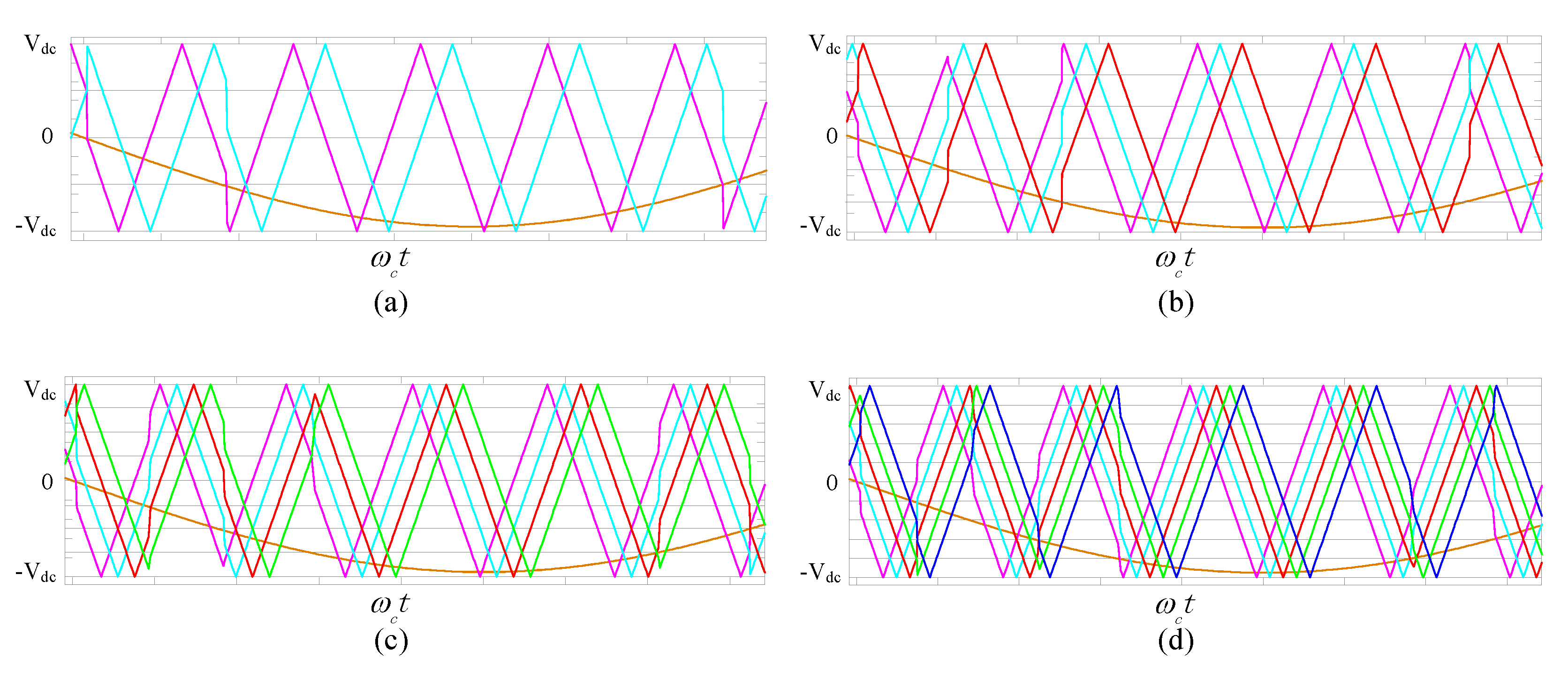
Figure 6 shows carriers and reference for the optimized new strategy under CHB inverters of various levels. It is clear that when the reference crosses the dotted line (boundary line) to enter into another interval, a sudden change of the carriers occurs and the carriers are thus shifted forward a certain phase to obtain phase continuity of the equivalent carrier. It should be noted that the carriers, after a sudden phase change for the new strategy, results from the already generated carriers but not from the carriers of PS-PWM. In addition, the actual carriers’ frequency is slightly higher than 1 kHz because of the forward adjustment of the original carriers. For a clear illustration, only half of the carriers are depicted in Figure 6. The remains are just phase inverted by 180° of that presented below.
Figure 7 shows the phase voltage and line voltage for phase-shifted PWM and the optimized new modulation strategy. The shapes of phase voltage for both modulation strategies look similar, but the line voltage for the optimized new modulation strategy is neater than that for phase-shifted PWM and keeps favorable stepped waveforms like the phase voltage. The stepped waveforms of line voltage also are a clear sign that the equivalent carrier of each phase was kept in phase fairly well.
Figure 8a,b show the spectrum of phase voltage for phase-shifted PWM and the optimized new modulation strategy, respectively. It is clear that under the optimized new modulation strategy more harmonic energy is injected into the phase voltage than that under phase-shifted PWM, and most of the harmonics center around the first carrier. Figure 8d shows that the harmonics around the first carrier are almost canceled in line voltage, as expected. However, for the line voltage of phase-shifted PWM, most harmonics are still retained. From this aspect, the optimized new modulation strategy achieves the anticipated results.
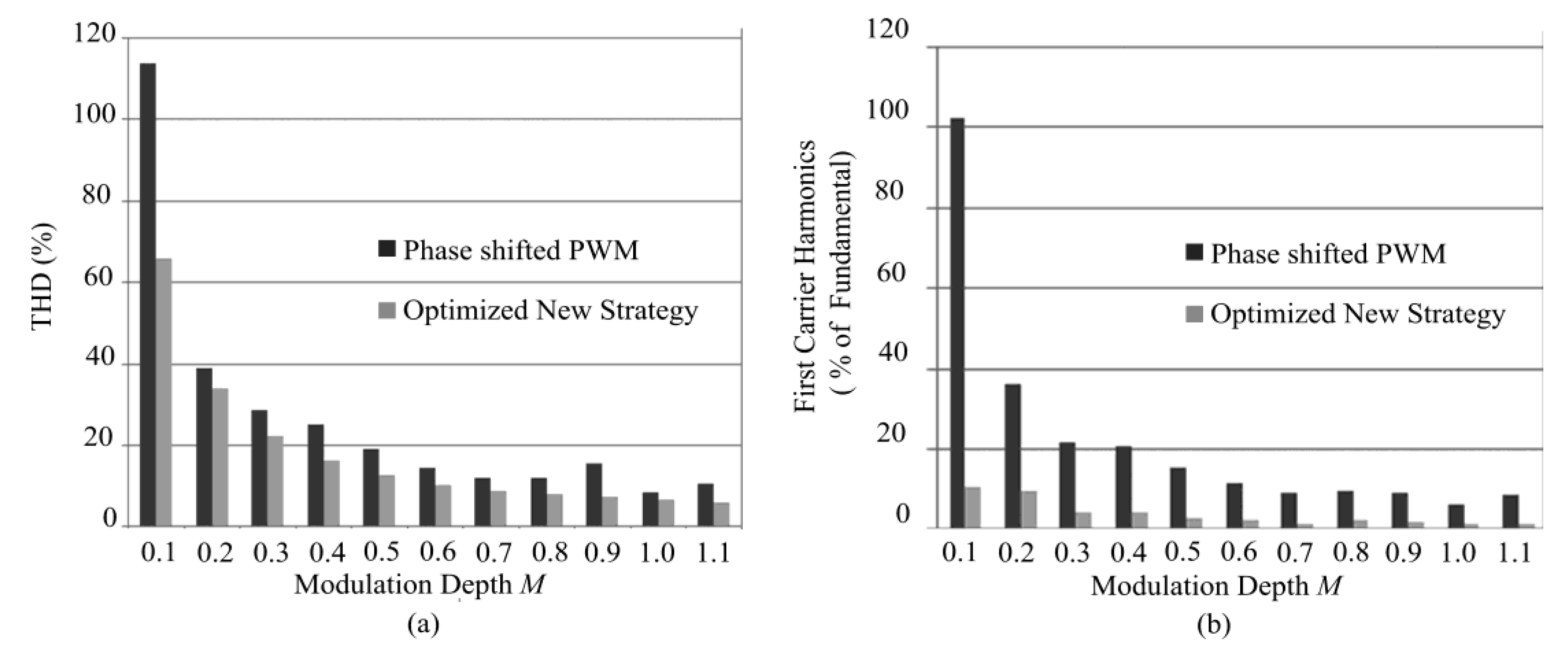
Figure 9a,b offer a detailed comparison of both modulation strategies on the performance of output line voltages. Obviously, the new modulation strategy achieves an improved total harmonic distortion (THD) and shows a sharp advantage to canceling the first carrier harmonics compare to phase-shifted PWM.
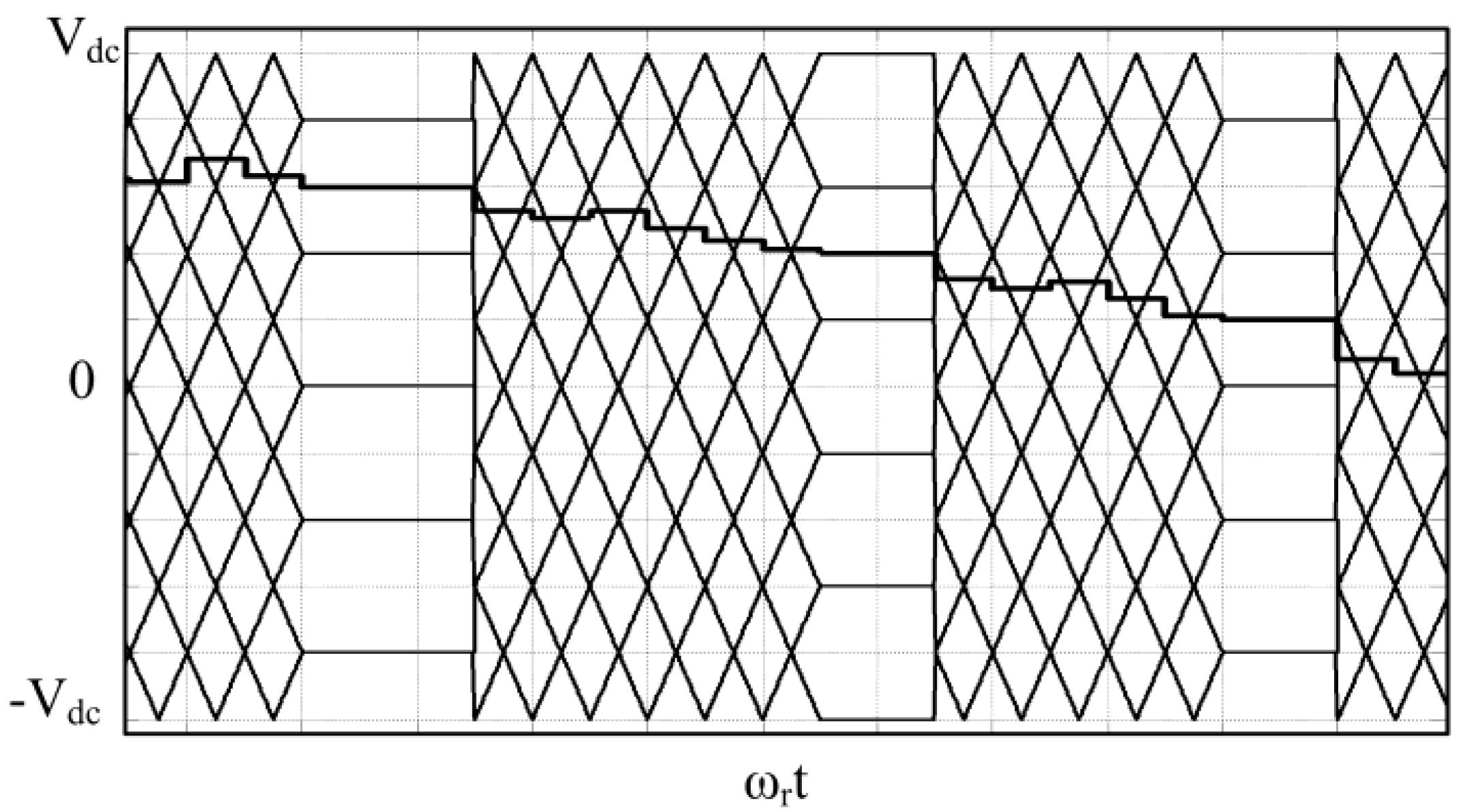
Figure 10 shows the carriers and reference under discontinuous modulation where . Unlike the carriers shown in Figure 6, the carriers under discontinuous modulation are kept unchanged in certain time intervals to avoid the intersections of the carriers and the reference. It is apparent that no switching transitions will be generated for the time this phase is designated to eliminate its state in the switching sequence.
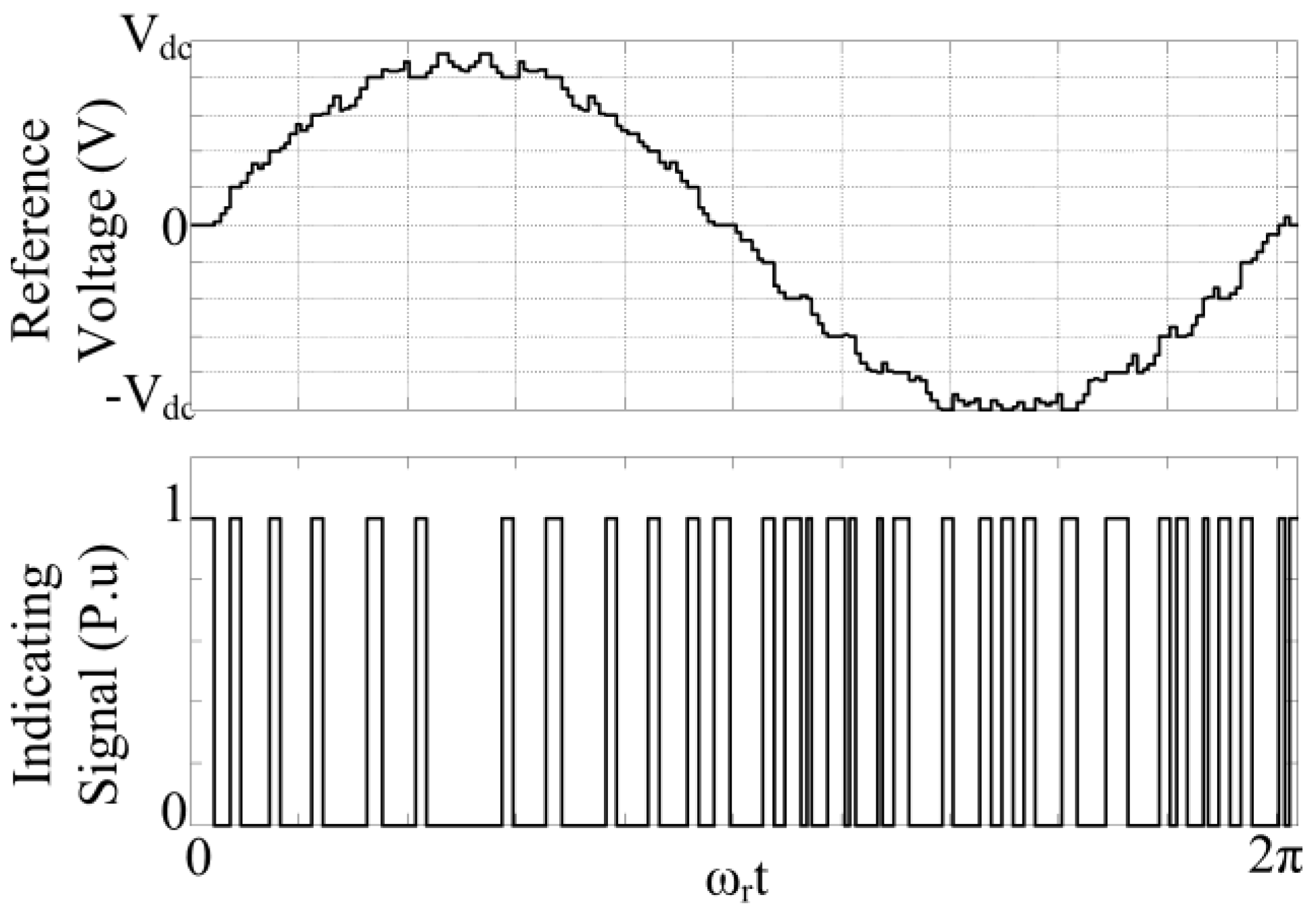
Figure 11 shows one phase reference voltage in a cycle for discontinuous modulation where the last switching transitions are eliminated, and a corresponding signal that indicates the state and whether this phase is the last crossing the common carrier. When the signal turns 1, this phase is the last crossing the common carrier and no switching should occur in power cells of this phase. It is clear that the indicating signal alters quickly from 1 to 0 or 0 to 1, which confirms that the state is the first crossing the common carrier or the last crossing the common carrier and rapidly rotates among three phases, which is mentioned in Section 2.3.
Figure 12 shows the phase voltage and line voltage under the discontinuous modulation. The phase voltage and line voltage still keep a fairly stair-like shape.
Figure 13 shows the output voltage of the power cell under continuous modulation and discontinuous modulation. The output voltage under continuous modulation consists of 13 pulses in one cycle. The output voltage under discontinuous modulation consists of nine pulses in one cycle. It is clear that the discontinuous modulation can greatly reduce the frequency of the switch.
3.2. Experimental Results
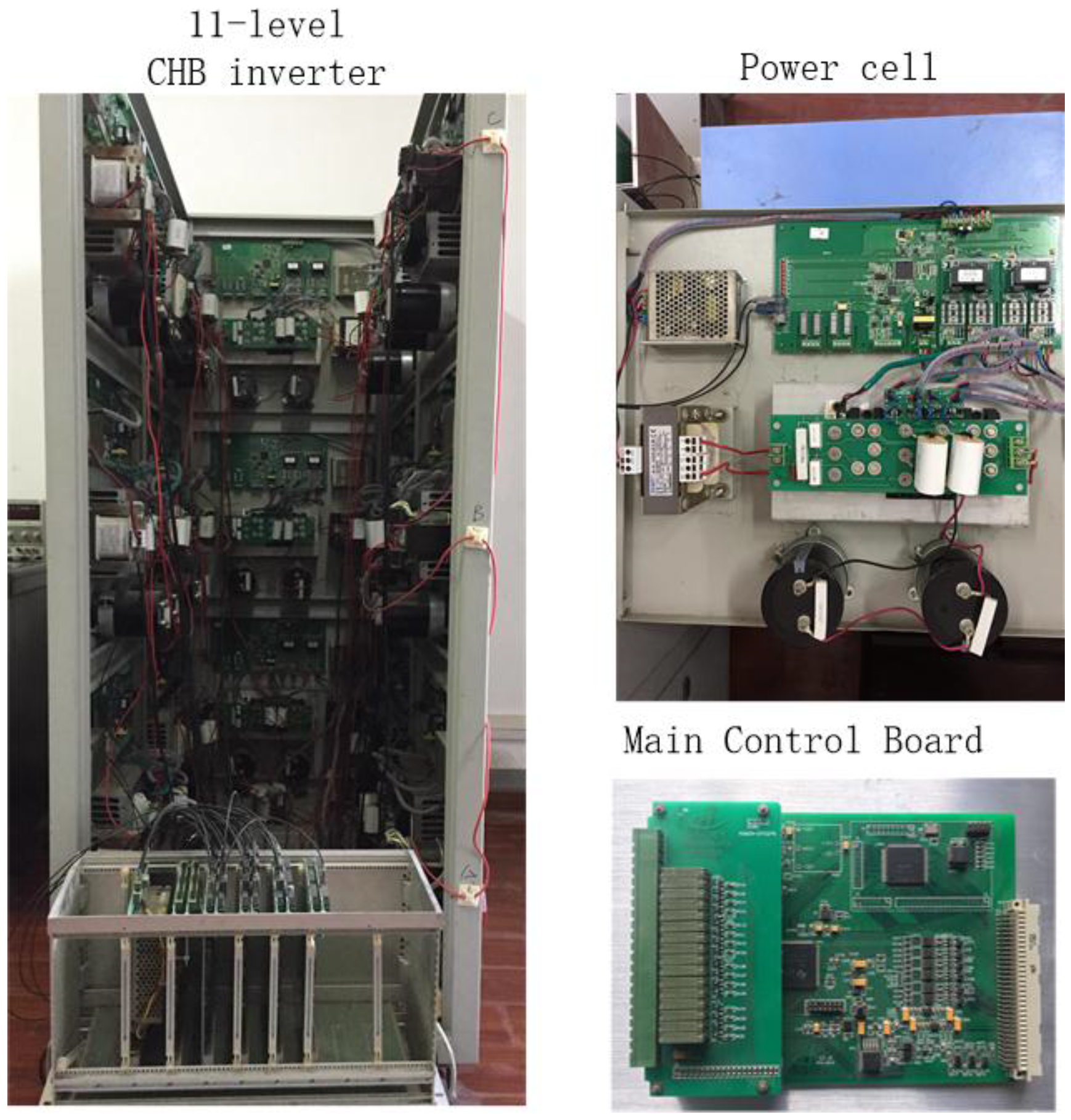
To confirm the feasibility and the validity of the proposed modulation strategy, a three-phase, 11-level CHB inverter is established. The switching frequency for carriers is about 610 Hz and the reference voltage frequency is 50 Hz. Figure 14 shows the picture of the experimental prototype. Table 2 provides the detailed parameters for experiments.
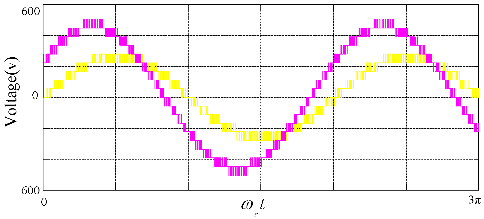
Figure 15 shows the experimental phase voltage and line voltage under the optimized new modulation strategy. It can be seen that the shapes of both output voltage are consistent with the simulation results shown above.
Figure 16 shows the experimental phase voltage and line voltage under discontinuous modulation with the mode eliminating the last state in the space vector. The number of phase voltage pulses is reduced distinctly compared to that shown in Figure 12. But there is no significant difference between line voltages for discontinuous modulation and the optimized new strategy.
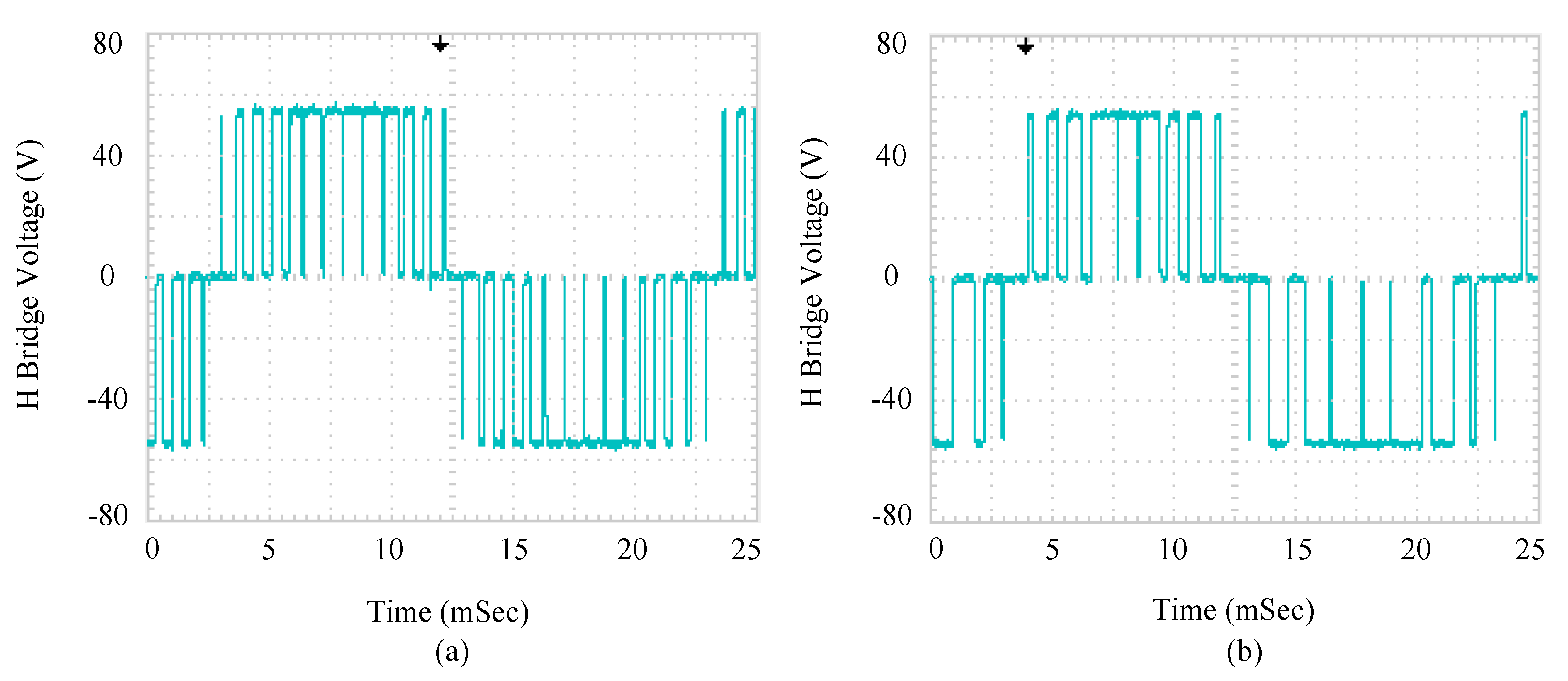
Figure 17a shows the output voltage of one power cell under the optimized new modulation strategy. Figure 17b shows the output voltage of one power cell under discontinuous modulation. Carefully observing Figure 17a,b, we find that the number of output voltage pulses for discontinuous modulation is about two thirds of that for the optimized new strategy, which confirms that the switching frequency of power semiconductor has decreased by the theoretical factor of one third.
4. Conclusions
The relationship between PS-PWM and PD-PWM is well established by introducing the new concept of the equivalent carrier. The concept could easily be applied to other multilevel modulation strategies and allow the quick establishment of the relationship between them.
A modulation strategy combining the PS-PWM and PD-PWM is proposed to improve the quality of output line voltage performance for CHB inverters. A discontinuous modulation strategy that could reduce the switching frequency to the theoretical value is offered for multilevel inverters as well. These two strategies are the embodiments of a way of new thinking, which entails adjusting the carriers to obtain improved performance of modulation strategy. Evidently, this way of thinking also has a role in improving other modulation strategies.
Detailed simulation and experimental results are offered to support the modulation strategy presented in this paper.
Acknowledgments
This work was supported by the National Natural Science Foundation of China (NSFC) under Grant No. 51677063 and Postdoctoral Innovative Talent Support Program of China.
Author Contributions
All the authors conceived and designed the study. Muxuan Xiao, Qianming Xu performed the simulation and the experiment and wrote the manuscript with guidance from Honglin Ouyang. Muxuan Xiao, Qianming Xu and Honglin Ouyang reviewed the manuscript and provided valuable suggestions.
Conflicts of Interest
The authors declare no conflict of interest.
References
- Lai, J.S.; Peng, F.Z. Multilevel converters—A new breed of power converters. IEEE Trans. Ind. Appl. 1996, 32, 509–517. [Google Scholar]
- Malinowski, M.; Gopakumar, K.; Rodriguez, J.; Pérez, M.A. A survey on cascaded multilevel inverters. IEEE Trans. Ind. Electron. 2010, 57, 2197–2206. [Google Scholar] [CrossRef]
- Miguel, M.; Francisco, H. A Comparison of modulation techniques for modular multilevel converters. Energies 2016, 9, 1091. [Google Scholar] [CrossRef]
- Xiongmin, T.; Zhang, J. A switching frequency optimized space vector pulse width modulation (SVPWM) scheme for cascaded multilevel inverters. Energies 2017, 10, 725. [Google Scholar] [CrossRef]
- Liang, Y.Q.; Nwankpa, C.O. A new type of STATCOM based on cascading voltage source inverters with phase-shifted unipolar SPWM. IEEE Trans. Ind. Appl. 1998, 35, 1447–1453. [Google Scholar]
- McGrath, B.P.; Holmes, D.G. Multicarrier PWM strategies for multilevel inverters. IEEE Trans. Ind. Electron. 2002, 49, 858–867. [Google Scholar] [CrossRef]
- Li, Y.; Wang, Y.; Li, B.Q. Generalized theory of phase-shifted carrier PWM for cascaded H-bridge converters and modular multilevel converters. IEEE J. Emerg. Sel. Top. Power Electron. 2016, 4, 589–605. [Google Scholar] [CrossRef]
- Marquez, A.; Leon, J.I.; Portillo, R.; Vazquez, S.; Franquelo, L.G.; Kouro, S. Adaptive phase-shifted PWM for multilevel cascaded H-bridge converters for balanced or unbalanced operation. In Proceedings of the IECON 2015—41st Annual Conference of the IEEE Industrial Electronics Society, Yokohama, Japan, 9–12 November 2015; pp. 5124–5129. [Google Scholar]
- Deng, F.; Chen, Z. Voltage-balancing method for modular multilevel converters under phase-shifted carrier-based pulsewidth modulation. IEEE Trans. Ind. Electron. 2015, 62, 4158–4169. [Google Scholar] [CrossRef]
- Angulo, M.; Lezana, P.; Kouro, S.; Rodriguez, J.; Wu, B. Level-shifted PWM for cascaded multilevel inverters with even power distribution. In Proceedings of the Power Electronics Specialists Conference, Orlando, FL, USA, 17–21 June 2007; pp. 2373–2378. [Google Scholar]
- Naderi, R.; Rahmati, A. Phase-shifted carrier PWM technique for general cascaded inverters. IEEE Trans. Power Electron. 2008, 23, 1257–1269. [Google Scholar] [CrossRef]
- De Paris, J.M.; Nicolini, A.M.; Carnielutti, F.; Massing, J.; Pinheiro, H. Sorting algorithm for a PD modulation for a cascaded multilevel converter. In Proceedings of the 2015 IEEE 13th Brazilian Power Electronics Conference and 1st Southern Power Electronics Conference (COBEP/SPEC), Fortaleza, Brazil, 29 November–2 December 2015; pp. 1–6. [Google Scholar]
- Liu, H.; Ma, K.; Blaabjerg, F. Device loading and efficiency of modular multilevel converter under various modulation strategies. In Proceedings of the 2016 IEEE 7th International Symposium on Power Electronics for Distributed Generation Systems (PEDG), Vancouver, BC, Canada, 27–30 June 2016; pp. 1–7. [Google Scholar]
- Carrara, G.; Gardella, S.; Marchesoni, M.; Salutari, R.; Ciutto, G. A new multilevel PWM method: A theoretical analysis. IEEE Trans. Power Electron. 1992, 7, 497–505. [Google Scholar] [CrossRef]
- McGrath, B.P.; Holmes, D.G. A comparison of multicarrier PWM strategies for cascaded and neutral point clamped multilevel inverters. In Proceedings of the Power Electronics Specialists Conference, Galway, Ireland, 23 June 2000; pp. 674–679. [Google Scholar]
- Blasko, V. A hybrid PWM strategy combining modified space vector and triangle comparison methods. In Proceedings of the Power Electronics Specialists Conference, Baveno, Italy, 23–27 June 1996; pp. 1872–1878. [Google Scholar]
- Holmes, D.G. The general relationship between regular-sampled pulse-width-modulation and space vector modulation for hard switched converters. In Proceedings of the Industry Applications Society Annual Meeting, Houston, TX, USA, 4–9 October 1992; pp. 1002–1010. [Google Scholar]
- McGrath, B.P.; Holmes, D.G.; Lipo, T. Optimized space vector switching sequences for multilevel inverters. IEEE Trans. Power Electron. 2003, 18, 1293–1301. [Google Scholar] [CrossRef]
Figure 1.
Modulation strategies and the corresponding output voltages: (a) phase-shifted pulse width modulation (PS-PWM) and phase disposition pulse width modulation (PS-PWM); (b) PD-PWM; (c) New strategy; (d) Output voltage for PS-PWM; (e) Output voltage for PD-PWM; (f) Output voltage for new strategy.

Figure 2.
Illustration of the cases that the reference crosses the carrier four times in a cycle of the carries after a negative phase shift of the carriers: (a) Positive phase shift; (b) Negative phase shift.
Figure 2.
Illustration of the cases that the reference crosses the carrier four times in a cycle of the carries after a negative phase shift of the carriers: (a) Positive phase shift; (b) Negative phase shift.
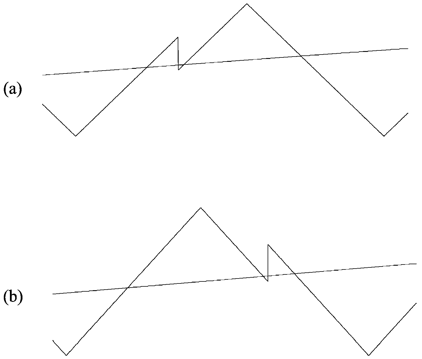
Figure 3.
Phase deviation of equivalent carriers between (phase A, B) caused by the different initial position of references.
Figure 3.
Phase deviation of equivalent carriers between (phase A, B) caused by the different initial position of references.
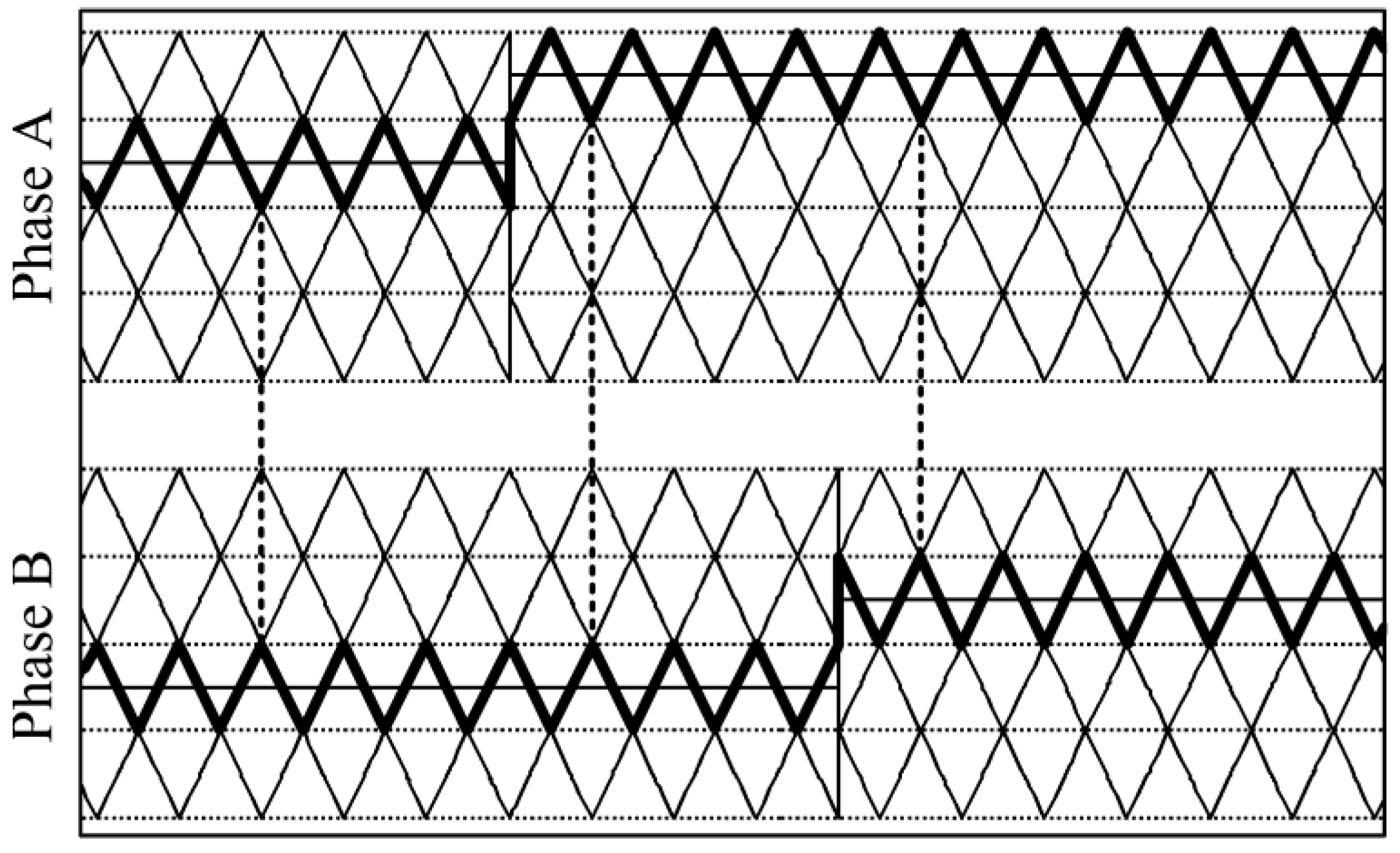
Figure 4.
The spectrum of line voltage for a five-level cascaded H-bridge (CHB) inverter under different condition. Switching frequency is 1 kHz. Modulation depth, M = 0.95. Reference frequency is 50 Hz: (a) Harmonics profile of line voltage where the equivalent carriers for phase A and B are opposite in phase; (b) Harmonics profile of line voltage where the equivalent carriers for phase A and B are in phase.

Figure 5.
The common carrier and the new references , and .
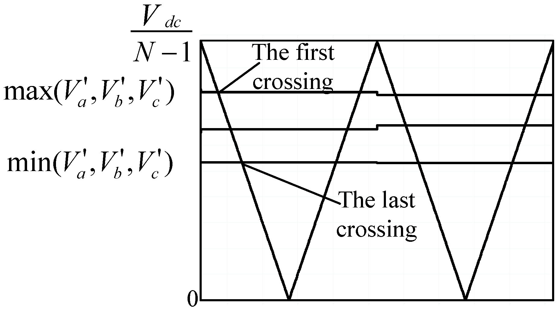
Figure 6.
Carriers and reference under the optimized new strategy under CHB inverters of various levels. (a) New strategy for five-level CHB inverter; (b) New strategy for seven-level CHB inverter; (c) New strategy for nine-level CHB inverter; (d) New strategy for 11-level CHB inverter.
Figure 6.
Carriers and reference under the optimized new strategy under CHB inverters of various levels. (a) New strategy for five-level CHB inverter; (b) New strategy for seven-level CHB inverter; (c) New strategy for nine-level CHB inverter; (d) New strategy for 11-level CHB inverter.

Figure 7.
Phase voltage and line voltage for PS-PWM and the optimized new strategy: (a) Phase voltage and line voltage for PS-PWM; (b) Phase voltage and line voltage for the optimized new strategy.
Figure 7.
Phase voltage and line voltage for PS-PWM and the optimized new strategy: (a) Phase voltage and line voltage for PS-PWM; (b) Phase voltage and line voltage for the optimized new strategy.

Figure 8.
Spectrum of phase voltage and line voltage for PS-PWM and the optimized new strategy (Modulation depth, M = 0.95): (a) Spectrum of phase voltage for PS-PWM; (b) Spectrum of phase voltage for the optimized new strategy; (c) Spectrum of line voltage for PS-PWM; (d) Spectrum of line voltage for the optimized new strategy.
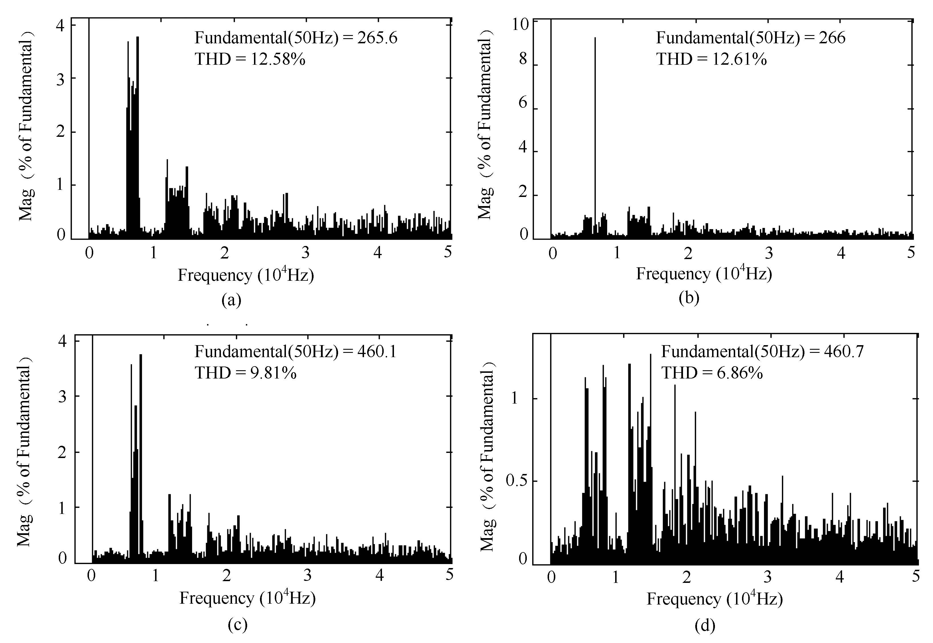
Figure 9.
Detailed comparison of the THD and first carrier harmonics about the line voltage PS-PWM and the optimized new strategy: (a) Comparison of THD; (b) Comparison of first carrier harmonics.
Figure 9.
Detailed comparison of the THD and first carrier harmonics about the line voltage PS-PWM and the optimized new strategy: (a) Comparison of THD; (b) Comparison of first carrier harmonics.

Figure 10.
Carriers and reference under the discontinuous modulation.

Figure 11.
Reference and indicating signal under the discontinuous modulation.

Figure 12.
Phase and line voltage under the discontinuous modulation.

Figure 13.
The output voltage of the power cell under continuous modulation and discontinuous modulation. (a) Output voltage under continuous modulation; (b) Output voltage under discontinuous modulation.
Figure 13.
The output voltage of the power cell under continuous modulation and discontinuous modulation. (a) Output voltage under continuous modulation; (b) Output voltage under discontinuous modulation.

Figure 14.
Picture of the experimental prototype.

Figure 15.
Experimental phase voltage and line voltage under the optimized new strategy (Modulation depth, M = 0.95).
Figure 15.
Experimental phase voltage and line voltage under the optimized new strategy (Modulation depth, M = 0.95).
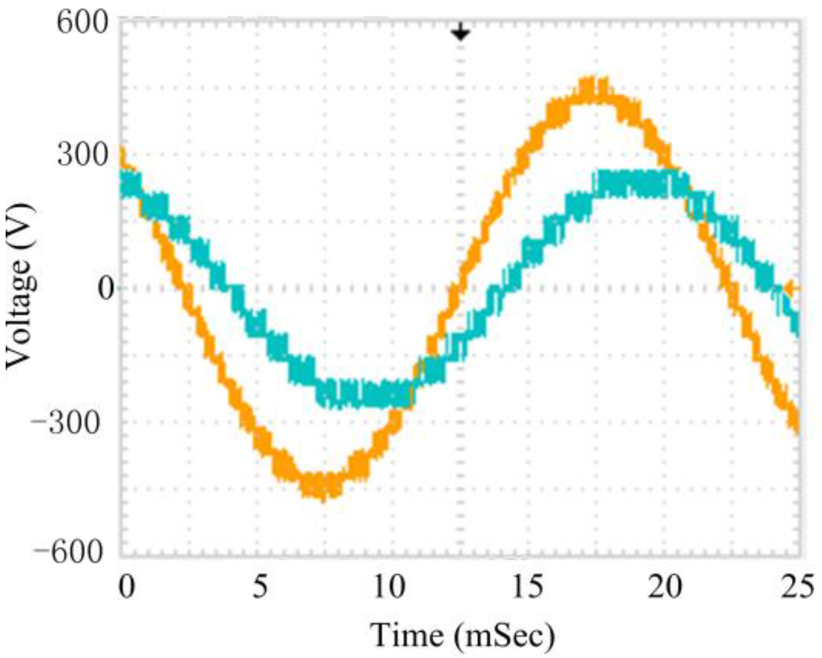
Figure 16.
Experimental phase voltage and line voltage under discontinuous modulation strategy (Modulation depth, M = 0.95).
Figure 16.
Experimental phase voltage and line voltage under discontinuous modulation strategy (Modulation depth, M = 0.95).
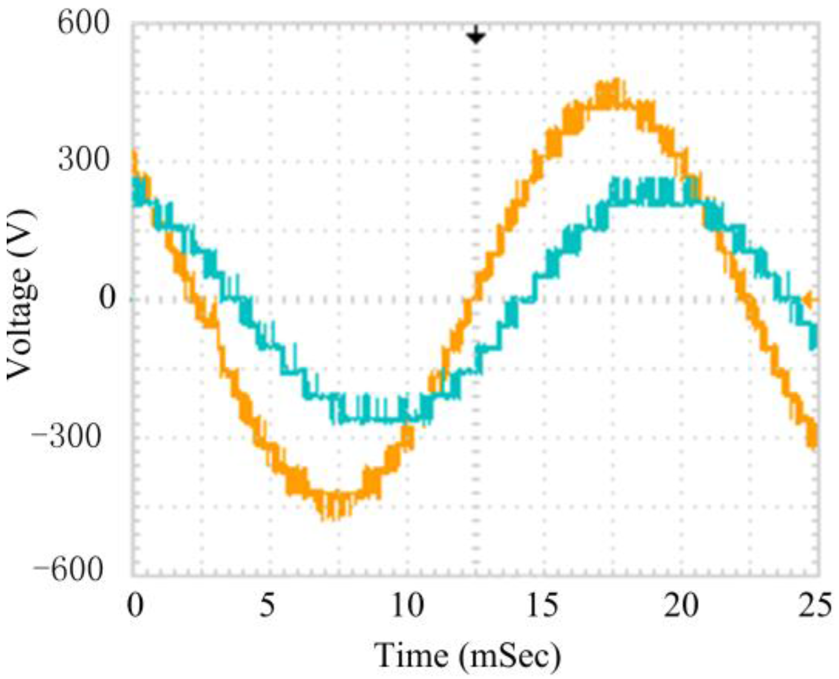
Figure 17.
Output voltages of one power cell under the optimized new strategy and discontinuous modulation strategy (Modulation depth, M = 0.95): (a) Output voltage under the optimized new strategy; (b) Output voltage under discontinuous modulation strategy.
Figure 17.
Output voltages of one power cell under the optimized new strategy and discontinuous modulation strategy (Modulation depth, M = 0.95): (a) Output voltage under the optimized new strategy; (b) Output voltage under discontinuous modulation strategy.


Table 1.
Parameters for simulation.
| Parameters | Value |
|---|---|
| Level of CHB Inverter | 5,7,9,10 |
| DC Link Voltage | 56 V |
| Output Voltage | 0–550 V (3-ph) |
| Max Modulation Depth | 1.15 |
| Switching Frequency | 610 Hz |
Table 2.
Parameters for Experiment.
| Parameters | Value |
|---|---|
| Number of Power Cells | 3 × 5 unit |
| DC Link Voltage | 56 V |
| Output Voltage | 0–550 V (3-ph) |
| Max Modulation Depth | 1.15 |
| Switching Frequency | 610 Hz |
| Insulated Gate Bipolar Transistor (IGBT) | 2MBI100VA-120-50 |
| Drivers | 2SD315-17 |
| Digital Signal Process (DSP) | TMS320F2812 |
| Field—Programmable Gate Array (FPGA) | Altera EPF10K20T |
© 2017 by the authors. Licensee MDPI, Basel, Switzerland. This article is an open access article distributed under the terms and conditions of the Creative Commons Attribution (CC BY) license (http://creativecommons.org/licenses/by/4.0/).
Share and Cite
MDPI and ACS Style
Xiao, M.; Xu, Q.; Ouyang, H. An Improved Modulation Strategy Combining Phase Shifted PWM and Phase Disposition PWM for Cascaded H-Bridge Inverters. Energies 2017, 10, 1327. https://doi.org/10.3390/en10091327
AMA Style
Xiao M, Xu Q, Ouyang H. An Improved Modulation Strategy Combining Phase Shifted PWM and Phase Disposition PWM for Cascaded H-Bridge Inverters. Energies. 2017; 10(9):1327. https://doi.org/10.3390/en10091327
Chicago/Turabian StyleXiao, Muxuan, Qianming Xu, and Honglin Ouyang. 2017. "An Improved Modulation Strategy Combining Phase Shifted PWM and Phase Disposition PWM for Cascaded H-Bridge Inverters" Energies 10, no. 9: 1327. https://doi.org/10.3390/en10091327
Note that from the first issue of 2016, this journal uses article numbers instead of page numbers. See further details here.