
An Isolated Three-Port Bidirectional DC-DC Converter with Enlarged ZVS Region for HESS Applications in DC Microgrids


1
School of Electrical Engineering and Automation, Tianjin University, Tianjin 300072, China
2
Electric Power Research Institute, State Grid Tianjin Electric Power Company, Tianjin 300384, China
*
Author to whom correspondence should be addressed.
Energies 2017, 10(4), 446; https://doi.org/10.3390/en10040446
Submission received: 15 February 2017
/
Revised: 20 March 2017
/
Accepted: 24 March 2017
/
Published: 1 April 2017
Abstract
:In this paper, a two-stage three-port isolated bidirectional DC-DC converter (BDC) for hybrid energy storage system (HESS) applications in DC microgrids is proposed. It has an enlarged zero-voltage-switching (ZVS) region and reduced power circulation loss. A front-end three-phase interleaved BDC is introduced to the supercapacitor (SC) channel to compensate voltage variations of SC. Consequently, wide ZVS range and reduced circulation power loss for SC and DC bus ports are achieved under large-scale fluctuating SC voltage. Furthermore, a novel modified pulse-width-modulation (PWM) and phase-shift (PHS) hybrid control method with two phase-shift angles is proposed for BA port. And it contributes to an increasing number of switches operating in ZVS mode with varying battery (BA) voltage. Phase shift control with fixed driving frequency is applied to manage power flow. The ZVS range as well as the current stress of resonant tanks under varying port voltages is analyzed in detail. Finally, a 1 kW prototype with peak efficiency of 94.9% is built, and the theoretical analysis and control method are verified by experiments.
1. Introduction
The development and utilization of renewable energy have turned out to be new solutions for the worldwide energy depletion and environmental pollution problems [1]. In order to achieve efficient utilization of distributed energy generations, DC microgrid has become a research focus in recent years [2,3,4]. However, the output of several renewable energy sources is intermittent and time-varying, and the load demand is uncertain [5]. Therefore, storage units are usually used to balance the power supplies and loads in DC microgrids. Several studies use hybrid energy storage systems (HESSs), which are composed of SC and BA, to improve stability and reliability of DC microgrid [6,7,8]. Numerous literatures have researched on energy management and power sharing strategy of HESS in DC microgrid [9,10,11,12,13,14,15,16]. While, the design of interface converters between HESS and DC microgirds is still considered as an emerging area of research.
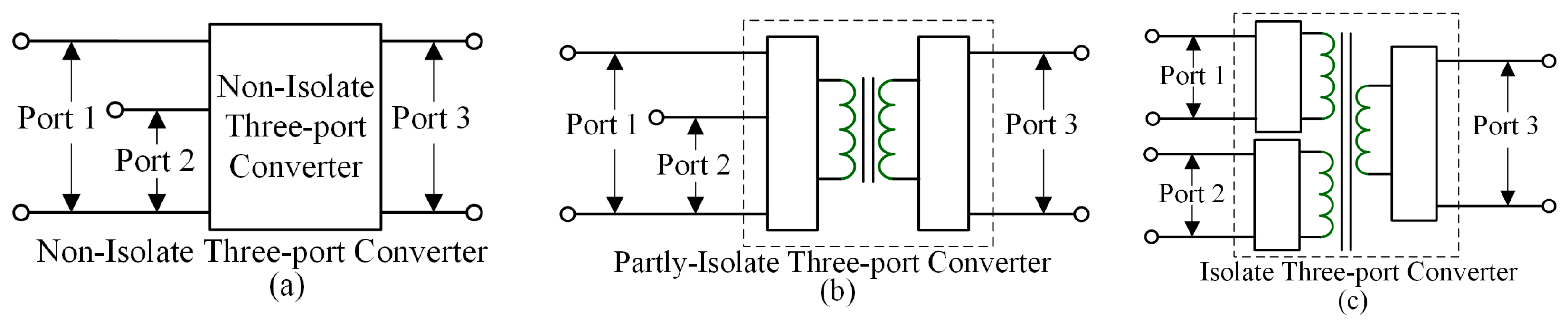
Three-port BDC, which integrates SC and BA converters into one dual-input converter, will assist to improve the efficiency, power density and control coordination of HESS converters. Many three-port BDCs have been reported in literatures. According to the connection methods, three-port BDCs can be categorized into three types: non-isolated, partly-isolated and isolated converters. Typical structures of three-port BDCs are shown in Figure 1 [17].
Figure 1a shows the diagram of non-isolated three-port converter [18,19], and Figure 1b presents the topology of partly-isolated converter [20,21,22]. The common shortcomings of non-isolated and partly-isolated three-port converters are the lack of complete electrical isolation among three ports, and being unable to cope with wide operating voltage ratio. For the HESS application, security is of great importance, and thus, electrical isolation is essential. In consequence, the isolated structure shown in Figure 1c is adopted in this article [23,24].
Numerous isolated three-port DC-DC converters have been proposed to integrate two energy sources into one dual-input converter. The three-port triple-active-bridge (TAB) converter shown in Figure 2, as the most widely disseminated isolated three-port topology, attracts a lot of attentions from researchers [23,24,25,26,27,28,29]. In [26], a TAB converter is used to deal with a hybrid energy source consisting of full cell and super capacitor. It appears that TAB converter has attractive features of galvanic isolation, bidirectional power flow, ZVS operation and phase shift control with fixed switching frequency. However, power transfer among three ports in TAB is coupled, therefore, decoupling control algorithm is required. What’s more, the power transmission of TAB topology is inversely proportional to the impedance of inductance. While, the inductance of TAB is inherent greater than the leakage inductor of transformer. In case of high power levels, switching frequency has to be reduced to get realizable inductance value. In [26,27,28,29] the driving frequency are all 20 kHz, and this will be detrimental for realizing high power density.
In order to solve problems of TAB mentioned above, a series-resonant (SR) based converter is proposed in [30]. The impedance of SR tank is determined by value of inductor and capacitor together with the switching frequency. Therefore, it can operate at higher frequency under high power level. In [31,32], renewable source, battery and load are integrated to a three-port SR BDC. The driving frequency is 100 kHz, which is apparently higher than 20 kHz of TAB as shown in [26,27,28,29]. What’s more, power flow among three ports can be controlled independently since there are only two SR tanks. Nevertheless, the three-port SR BDC still suffers disadvantages including losing ZVS operation and increased current stress under wide voltage variations. However, previously published works mainly concentrated on the operating characteristics of SR BDC with fixed port voltages. The methods, which can enlarge ZVS region and reduce circulation power loss under varying port voltages, are still considered as emerging area of research.
Two methods for enlarging ZVS range and decreasing power circulation loss under DAB and TAB topologies are reported in [33,34,35,36]. One method is to adopt improved control algorithm. Literature [34] has presented an improved modulation control approach, where two phase-shift angles are employed to minimize the switching losses for DAB under light load. Another alternative method is to use a front-end converter to keep input voltage of bridge constant, as suggested in [36]. These two methods effectively improve the characteristics of TAB converters with wide voltage variations. Unfortunately, few of literatures have ever investigated the validity of these two methods in three-port SR BDC under varying port voltages.
Based on the SR BDC, this article proposes a two-stage three-port BDC to integrate HESS and DC microgrid. The subject of this paper is to enlarge the ZVS operating range and to reduce the circulation power loss of the proposed three-port SR BDC. Then, by comprehensively considering the large SC’s and small BA’s voltage fluctuation ranges, two different methods are adopted in SC and BA channels respectively. For the SC channel, a three-phase interleaved BDC is introduced to convert the widely fluctuating VSC to a fixed voltage Vdc-link. This method guarantees the unity voltage gain between SC and DC bus ports. The BDC adopts the interleaved structure to improve the power level of the BDC, and to reduce the SC current ripple as well as the inductor size [37,38]. Additionally, a PWM and PHS (PWM-PHS) control method is developed to enlarge ZVS operating range when the voltage gain between DC bus and BA ports is greater than 1. The control objectives of three-port SR BDC and there-phase interleaved BDC are to maintain the DC bus voltage and dc-link voltage stable respectively. Finally, a prototype platform is built to verify the feasibility of the proposed topology. The structure of this article is organized as followings: the topology of proposed converter is given in Section 2. Operating principles are introduced in Section 3. Section 4 explains the variation of ZVS region and the peak value of resonant current under varying voltage gain. Principles of the proposed PWM-PHS control method are also introduced in Section 4. Finally, the experimental results are presented in Section 5, while the conclusion is drawn in Section 6. The main contributions of this paper are summarized below:
- (1)
- A new two-stage three-port isolated BDC topology is proposed to integrate SC and BA.
- (2)
- Methods to enlarge ZVS region and to reduce power circulation loss for three-port SR BDC under varying port voltages are first investigated.
- (3)
- A front-end converter in SC channel is introduced to keep input of full bridge constant. For BA channel, PWM-PHS control method is developed to improve the characteristics of the proposed three-port BDC.
- (4)
- By adopting the two-stage structure, all switches of SC and DC bus ports have realized ZVS with variable VSC. By applying the proposed PWM-PHS control method, two more switches of BA port realize ZVS even under the worst input voltage condition of MBA = 1.15.
2. Proposed System
The overall structure of the proposed two-stage three-port BDC is shown in Figure 3. It contains two parts: a three-port SR BDC and a three-phase interleaved BDC. Three-port SR BDC is presented to maintain DC bus voltage stable and to control power transmission among three ports. The function of three-phase interleaved BDC is converting the widely fluctuating super capacitor voltage Vsc to a constant voltage Vdc-link.
2.1. Three-Port SR BDC
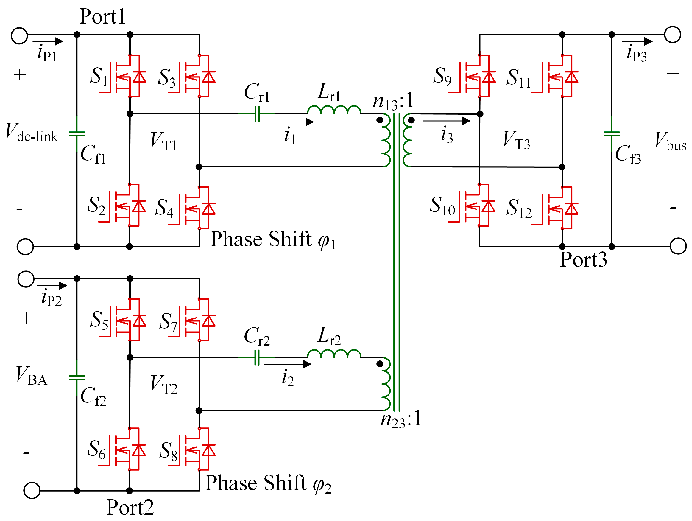
The three-port SR BDC is composed of a three-winding transformer, three full bridges and two SR tanks formed by Cr1, Lr1 and Cr2, Lr2 respectively. The three-winding transformer provides electrical isolation among three ports. What’s more it has inherent bidirectional power flow characteristic, since all power switches of three full bridges are MOSFETs. The converter works at a constant switching frequency fs, which is above the resonant frequency of SR tanks. As a consequence, it works only in continuous current mode. Phase shift control method is implemented, the amount and direction of transmitted power are controlled by the phase shift angles. All the switches of the three full bridges work with 50% duty cycle.
Through theoretical analysis, the three-port SR BDC is shown to have the best operating characteristics such as maximum ZVS operating region, reduced current stress and cutoff current only under unity voltage gain among three ports. Whereas, the voltage of SC has a large fluctuation range with the change of residual energy. To solve the contradictions of the varying VSC and the best operating voltage gain restraint of SR BDC, a three-phase interleaved BDC is applied in the system. The interleaved BDC is used to convert the widely fluctuating SC voltage to a fixed voltage Vdc-link. However, the fluctuation range of battery voltage is relatively small, the method of converting the battery voltage to a fixed voltage by increasing a BDC converter is not the best solution. In addition, a new PWM-PHS hybrid control strategy which has two phase-shift angles is proposed to improve the operation characteristics of battery channel under a variation range of voltage gain. The proposed control method can increase the number of MOSFETs operating in ZVS.
The features of the three-port SR BDC are:
- (1)
- Three-port structure with transformer coupling reduces amount of power switches, increases power density.
- (2)
- Power flow between BA port and DC bus port, SC port and DC bus port are bidirectional.
- (3)
- Centralized control method of power flow by changing the direction and magnitude of the phase shift angles between three ports is applied.
- (4)
- Three-phase interleaved BDC is introduced in the SC channel to keep voltage gain MSC = 1, which guarantee best operating characteristics of SC channel of SR BDC.
- (5)
- PWM-PHS hybrid control strategy is proposed for the BA channel to increase the number of switches, which can achieve ZVS, under a variation voltage VBA.
2.2. Three-Phase Interleaved BDC
A three-phase interleaved BDC is introduced to the SC channel of SR BDC to convert the widely fluctuating SC voltage VSC to a fixed voltage Vdc-link. The SC is connected to the low-voltage side, and the SR BDC is placed on the high-voltage side. When energy flows from SC to the SR BDC, it works at boost mode, and conversely, it works under buck mode.
A non-isolated bidirectional buck/boost converter topology is adopted in this paper. In order to achieve high efficiency and high power density, the converter is designed to operate in discontinuous conducting mode (DCM), such that all the switches realize ZVS, and the buck/boost inductors are minimized. However, the DCM also has the drawback of large current ripple. To reduce current ripple, the interleaved multi-phase structure is introduced to reduce current ripple. All of the interleaved channels adopt the same control strategy, while hold a phase shift of π/3 in driving signal from each other. As a consequence, the inductor currents of three phases are shifted by π/3. Hence, with interleaved inductor currents, the ripple current of SC is minimized. The features of the three-phase interleaved BDC are:
- (1)
- The structure is simple, and it combines a boost converter together with a buck converter connected in antiparallel.
- (2)
- Three-phase interleaved structure is adopted to reduce current ripple, improve power level and reduce current stress of the converter.
- (3)
- It works under DCM, which can reduce the inductance value.
- (4)
- Two MOSFETs of one phase-leg conduct complementarily, and the inductor operates under DCM condition, and thus ZVS of MOSFETs is achieved.
3. Operating Analysis
In this section, operating principles of three-port SR BDC and three-phase interleaved BDC are introduced respectively. For the three-port SR BDC, relationship between phase shift angle and power transmission is deduced. What’s more, ZVS soft-switching realizing region and current stress of the resonant tank are analyzed in detail. For three-phase interleaved BDC, the operating principle as well as the inductance designing method is introduced.
3.1. Operating Principle of Three-Port SR BDC
The proposed three-port SR BDC is shown in Figure 4. It is composed of three full bridges, a three-winding transformer, two SR tanks formed by Cr1 and Lr1, Cr2 and Lr2, and filter capacitors Cf1–Cf3. Port 1 is connected to SC through a three-phase interleaved BDC, port 2 is and port 3 are BA port and DC bus respectively. Phase shift method is applied among three ports to control the direction and magnitude of the power transmission, all the switches of the converter are driven at 50% duty cycle. Since the voltage of three ports are constant dc, VT1, VT2 and VT3 are square-waves with amplitudes of ±Vdc-link, ±VBA and ±Vbus respectively. In the subsequent analysis, phase shift angles of SC and BA ports are defined as φ1 and φ2, which are shown in Figure 4. They control the phase shift between the square-wave outputs of the active bridges. The phase shifts φ1 and φ2 are considered positive if VT1 and VT2 lead VT3, and conversely, φ1 and φ2 are considered negative.
3.1.1. Operating Mode Analysis
The operating principles when both SC and BA ports are providing energy to DC bus port are analyzed. In this condition both φ1 and φ2 are positive. The theoretical waveforms, when φ1 > φ2 > 0, are shown in Figure 5.
There are 18 different intervals in one switching cycle. Dead time is considered in the analysis, however, the charging and discharging intervals of snubber capacitors are very small, and they can be neglected.
Interval 1 (t0–t1): S1 and S4, S5 and S8 are on. This interval is dead time of port 3 and all the switches of port 3 are off. Since i3 is positive, i3 flows through the anti-parallel diodes of S9 and S12. i1 flows through S1 and S4, and i2 flows through S5 and S8. This interval ends at t1, when S9 and S12 are turned on.
Interval 2 (t1–t2): S1 and S4, S5 and S8, S9 and S12 are on. This interval ends when i2 increases to zero. The anti-parallel diodes of S9 and S12 conduct prior to the main switches, thus, S9 and S12 are turned on with ZVS. The operating characteristics of port 1 and 2 are exactly same with interval 1.
Interval 3 (t2–t3): This interval begins at t2 when i2 increases to zero, and it ends when switches S1 and S4 are turned off. During this interval, S1 and S4 of port 1, S5 and S8 of port 2 and S9 as well as S12 of port 3 are on. i1, i2 and i3 are positive and flow through S1 and S4, S5 and S8, and S9 and S12 respectively.
Interval 4 (t3–t4): This interval is dead time of port 1 and all the switches of port 1 are off. i1 is positive, so i1 flows through the anti-parallel diodes of S2 and S3. During this interval, i2 and i3 flow through S5 and S8, and S9 and S12 respectively. This interval ends when S2 and S3 are turned on.
Interval 5 (t4–t5): At t4, S2 and S3 are turned on, and this interval ends when S5 and S8 are turned off. Since the anti-parallel diodes conduct before main switches of S2 and S3, S2 and S3 are turned on with ZVS. The operating characteristics of port 2 and 3 are identical with interval 4.
Interval 6 (t5–t6): At t5, switches S5 and S8 are turned off, this interval ends when i1 decreases to zero. This interval is dead time of port 2 and all the switches of port 2 are off. i2 is positive, hence i2 flows through the anti-parallel diodes of S6 and S7. i1 and i3 flow through S2 and S3, and S9 and S12 respectively.
Interval 7 (t6–t7): This interval begins at t6 when i1 decreases to zero, and it ends when S6 and S7 are turned on. The difference between interval 7 and 6 is that the direction of i1 changes. i2 still flows through the anti-parallel diodes of S6 and S7.
Interval 8 (t7–t8): At t7, S6 and S7 are turned on, and this interval ends when i3 decreases to zero. The anti-parallel diodes conduct ahead the main switches of S6 and S7, therefore, S6 and S7 are turned on with ZVS. The operating characteristics of port 1 and 3 are exactly same with interval 7.
Interval 9 (t8–t9): This interval begins at t8 when i3 decreases to zero, and it ends when S9 and S12 are turned off. The difference between interval 9 and 8 is that the direction of i3 changes. The operating characteristics of port 1 and 2 are exactly the same with interval 8.
Interval 10 (t9–t10): This interval is dead time of port 3. Because i3 is negative, so i3 flows through the anti-parallel diodes of S10 and S11. During this interval, i1 and i2 flow through S2 and S3, and S6 and S7 respectively. This interval ends when S10 and S11 are turned on.
Interval 11 (t10–t11): At t10, S10 and S11 are turned on, and this interval ends when i2 decreases to zero. The anti-parallel diodes conduct before main switches of S10 and S11, so that S10 and S11 are turned on with ZVS. The operating characteristics of port 1 and 2 are exactly same with interval 10.
Interval 12 (t11–t12): This interval begins at t8 when i2 decreases to zero, and it ends when S2 and S3 are turned off. The difference between interval 12 and 11 is that the direction of i2 changes.
Interval 13 (t12–t13): This interval is dead time of port 1. During this interval, i1 is negative, so i1 flows through the anti-parallel diodes of S1 and S4. i2 and i3 flow through S6 and S7, and S10 and S11 respectively. This interval ends when S1 and S4 are turned on.
Interval 14 (t13–t14): At t13, S1 and S4 are turned on and this interval ends at t14 when S6 and S7 are turned off. The anti-parallel diodes conduct prior to the main switches of S1 and S4, so S1 and S4 are turned on with ZVS. The operating characteristics of port 2 and 3 are exactly same with interval 13.
Interval 15 (t14–t15): This interval is dead time of port 2. During this interval, i2 is negative, thus i2 flows through the anti-parallel diodes of S5 and S8. i1 and i3 flow through S1 and S4, and S10 and S11 respectively. This interval ends at t15 when i1 increases to zero.
Interval 16 (t15–t16): This interval begins at t15 when i1 increases to zero and ends when S5 and S8 are turned on. This interval is still dead time of port 2. The difference between interval 16 and 15 is that the direction of i1 changes.
Interval 17 (t16–t17): This interval begins at t16 when S5 and S8 are turned on, and ends when i3 increases to zero. Because the anti-parallel diodes conduct prior to the main switches of S5 and S8, so S5 and S8 are turned on with ZVS. The operating characteristics of port 1 and 3 are exactly same with interval 16.
Interval 18 (t17–t18): This interval begins at t17 when i3 increases to zero, and ends when S10 and S11 are turned off. The difference between interval 18 and 17 is that the direction of i3 changes.
3.1.2. Analysis for Voltage Source Load
This section analyzes the relationship between phase shift angle and power transmission, ZVS soft-switching realizing condition and peak current of the resonant tank under a given voltage source load.
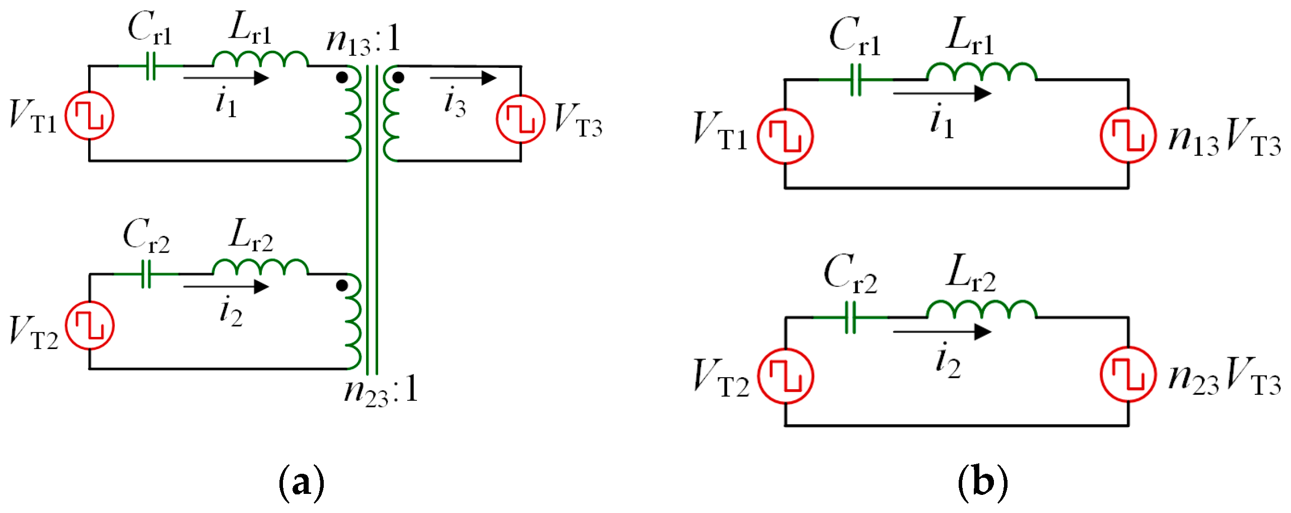
The equivalent circuits of the three-port SR BDC are shown in Figure 6. In Figure 6a the output of three active bridges are represented by square waves VT1, VT2 and VT3 respectively, and in Figure 6b VT3 of port 3 is transferred to port 1 and port 2 according to the transformer ratio.
In the proposed three-port SR BDC, Lr1 = Lr2 = Lr, Cr1 = Cr2 = Cr, and the resonant frequency of SR tanks are fr. The operating frequency of three ports is fs, which is greater than fr, and the corresponding angular velocity is ωs. Then the impedance value of two resonant tanks can be given by:
The Fundamental Harmonics Approximation (FHA) method is a commonly used approach for steady-state analysis in resonant-type converters. And the accuracy level of the results obtained from FHA is acceptable for our work. To simplify the analysis procedure, all harmonics except fundamental component of all voltages and currents are neglected. VT1,1, VT2,1 and VT3,1 are the fundamental components of square waves VT1, VT2 and VT3, and phase shift angles between port 1 and port 3, port 2 and port 3 are φ1 and φ2 respectively. Using the Fourier series, VT1,1, VT2,1 and VT3,1 are shown as follows:
The variables MSC and MBA are defined as the voltage gain between port 1 and port 3, port 2 and port 3 respectively. They are given by (5) and (6):
Resonant currents of three ports can be obtained as follows:
Switches in port 1 and port 2 can realize ZVS only when the resonant tank currents lag their applied square wave voltages. While for port 3, the defined positive current direction is contrary to port 1 and 2, the condition for ZVS realization is that the resonant current leads its applied square wave voltage. Then the constraint conditions for ZVS of port 1–3 can be given by (10)–(12) respectively:
By calculating the maximum value of i1(t) and i2(t), the peak current of two resonant tanks can be derived as:
The transferred power from SC and BA ports to the bus port can be calculated as follows:
Equations (15) and (16) indicate that the power transferred from SC and BA ports to the DC bus port are proportional to the sinusoidal values of φ1 and φ2 respectively. It is obviously that the power transmission is positive when φ1 and φ2 values are positive, and conversely the power flow is negative.
3.1.3. Analysis for Resistive Load
This section explains the relationship of voltage gain, power transmission and phase shift angles under a resistive load. If the DC bus port is connected to a pure resistive load, the output voltage Vbus needs to be derived. According to superposition theorem, in the three-port SR BDC with linear resistive load, the output voltage Vbus can be divided into two parts: VbusSC and VbusBA. VbusSC and VbusBA are output voltage values when only one of the two inputs works alone. MbusSC and MbusBA are the corresponding voltage gain, and are given by:
Under specific output voltage value and phase shift angles conditions, the transferred power is given in (15) and (16), no matter what kind of load is connected to the DC bus port. If the load resistance is defined as RL. Combing (15) and (16), the output power P1 and P2, when Vdc-link and VBA work alone, can be given by:
By combing (17)–(20), the voltage gain MbusSC and MbusBA can be given as follows:
According to the superposition theorem, the output voltage Vbus with resistive RL can be given by:
3.2. Operating Principle of Three-Phase Interleaved BDC
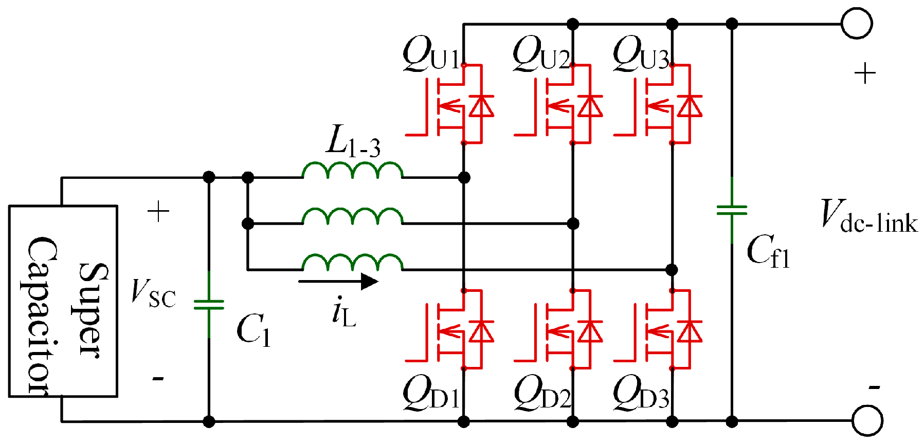
The operating principles of the three-phase interleaved BDC are analyzed in this section. The proposed three-phase interleaved BDC is shown in Figure 7. When power transfers from SC to the dc-link, it works under boost mode and switches QD1–QD3 are main switches. If direction of power transfer is reversed, the BDC works under buck mode and switches QU1–QU3 are main switches. L1–L3 are buck/boost inductors, C1 and Cf1 are filter capacitors. By adopting three-phase interleaving structure, current ripple of SC port can be minimized and thus the required filter capacitance can be reduced.
For the proposed three-phase interleaved BDC, switches of one phase leg conduct complementarily, and the inductor current can go through from positive to negative and then raise to positive. This will ensure all the switches realize ZVS turn on.
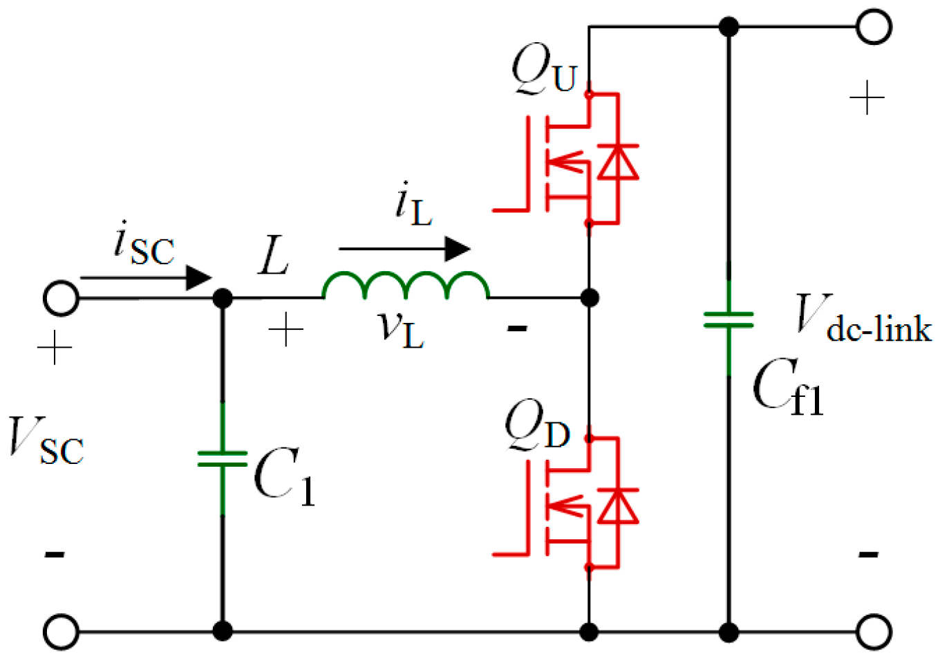
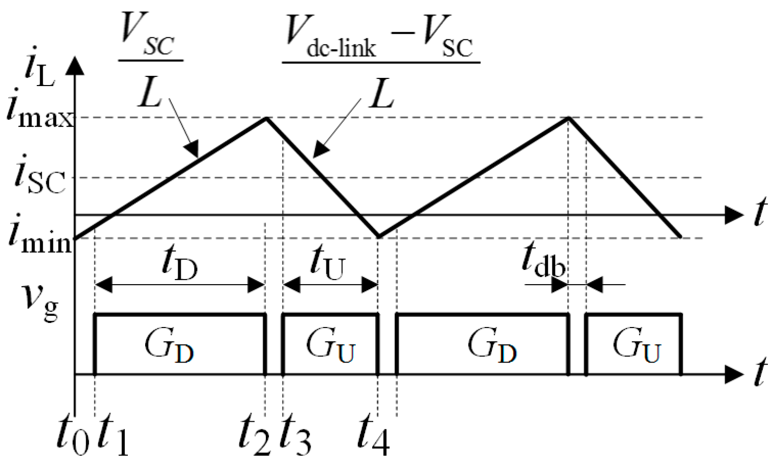
The three-phase interleaved channels adopt the same control strategy, but hold a phase shift of π/3 in driving signal. In order to simplify the analysis, the operating characteristics of single phase are introduced. Circuit diagram of single phase is shown in Figure 8, and theoretical waveforms under boost mode are shown in Figure 9.
The parameters are defined as follows: VSC and Vdc-link are the voltage of SC and dc-link; iL and vL are voltage and current of the buck/boost inductor L; imax and imin are the maximum and minimum value of iL respectively; Δi is the variation of iL during one switching cycle; iSC is the current of SC. tdb is dead band time; Ts is switching period; tD and tU are the conducting time of QU and QD separately.
For single-phase BDC, there are four different intervals in one switching cycle. Same as the above analysis of three-port SR BDC, dead time is considered, while charging and discharging intervals of snubber capacitors are neglected.
Interval 1 (t0–t1): This interval is dead band time, both QU and QD are off, and it ends when QD is turned on. During this interval, iL < 0 and it flows through the anti-parallel diode of QD. If the conduction voltage drop of anti-parallel diode is neglected, vL = VSC and iL increases linearly.
Interval 2 (t1–t2): During this interval, QD is on and QU is off, iL flows through QD. Since the anti-parallel diodes conduct prior to the main switches of QD, thus it is turned on with ZVS. Same as interval 1, iL increases linearly.
Interval 3 (t2–t3): This interval is also dead band time, both QU and QD are off, and it ends when QU is turned on. Different from interval 1, during this interval iL > 0, so it flows through the anti-parallel diode of QU. vL = VSC − Vdc-link and this value is less than zero, so iL decreases linearly.
Interval 4 (t3–t4): During this interval, QU is on and QD is off. iL flows through QU. Same as interval 3, iL decreases linearly. Since the anti-parallel diodes conduct before main switches of QU, it is turned on with ZVS.
Compared to tD and tU, tdb can be ignored, so Δi can be derived as follows:
To maintain ZVS switching of QU and QD, it must be ensured that imax > 0 and imin < 0.
4. ZVS Region Analysis and Proposed Method for Expanding ZVS Realization Range
Since the transformer voltage of port 3 is clamped by the output voltage Vbus, so there is no direct energy interaction between port 1 and port 2. Thus, the three-port SR BDC can be decomposed into two single input SR BDCs. The ZVS realization and current stress of single channel SR BDC can provide reference for the three-port SR BDC. To simplify the analysis, the ZVS realization region and current stress of single channel SR BDC are analyzed in this section.
4.1. ZVS Region and Current Stress Analysis of Single Channel SR BDC
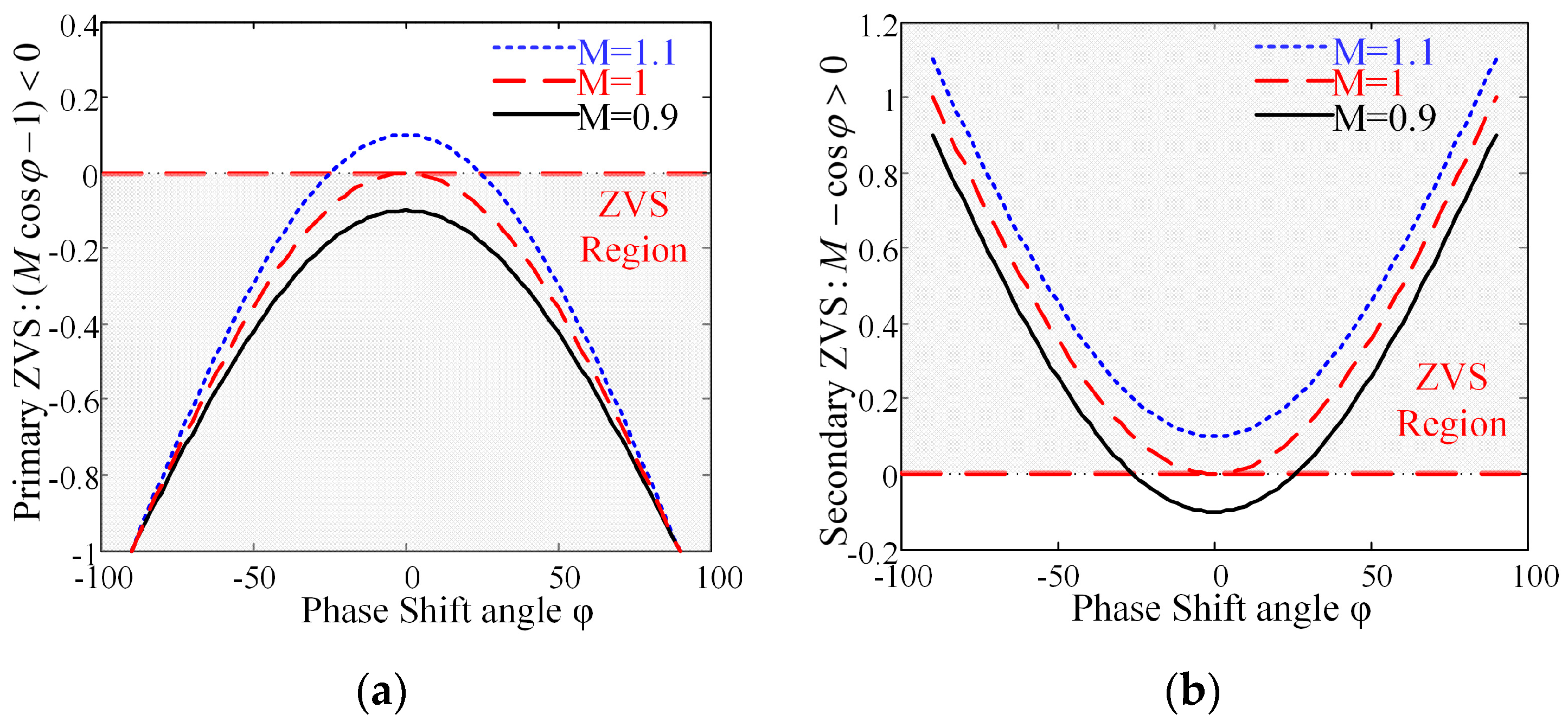
Through (10)–(12), the ZVS constraint conditions for primary-side and secondary-side can be simplified as follows:
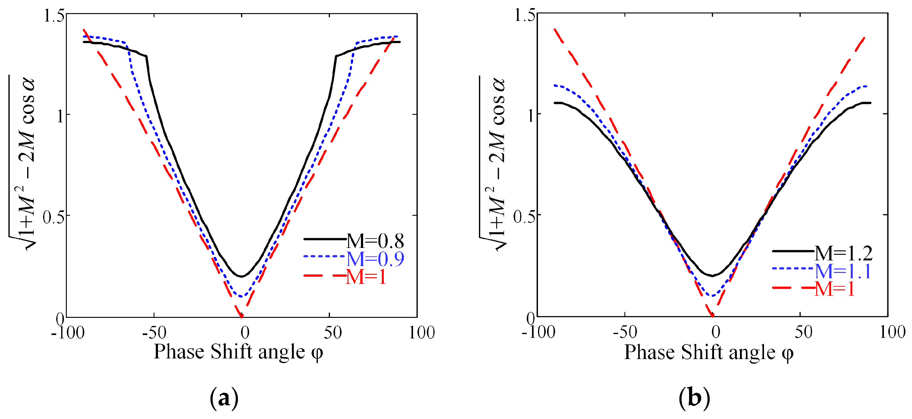
The ZVS regions of primary and secondary sides of single channel SR BDC are shown in Figure 10a,b, respectively. Figure 10a shows that when M < 1 all switches of primary side can realize ZVS, while as shown in Figure 10b, switches of secondary side can only realize ZVS when φ is greater than a certain value. When M > 1 situations are just contrary to situations when M < 1. It can be obtained that, the ZVS realization regions of primary and secondary sides change reversely under varying M. So during the design process, M should be as close to 1 as possible, and M = 1 is the best choice to achieve ZVS for all the switches of primary and secondary sides.
Before analyzing the peak value of resonant current under varying M, it must be noticed that phase shift angles to transfer same power under different M are varying. If we suppose that the phase shift angle under unity voltage gain (M = 1) is φ, and the phase shift angel to transfer same power under varying M is α. The relationship between φ and α is shown in (27) and (28). It is shown in (13) and (14) that with certain input voltage, resonant parameters and switching frequency, the peak value of resonant current is directly proportional to N which is shown in (29). The diagrams of N under M < 1 and M > 1 are shown in Figure 11a,b, respectively:
Figure 11 shows that, when M < 1, the peak current of resonant tanks increases with the decreases of M in a large range. While when M > 1, the peak current increases with the increases of M in a certain range. In the design process, the phase shift must be limited in a relatively small range to restrict cut off current of switches. So, from the point of limiting peak value of resonant current, M should be designed as close to 1 as possible. And M = 1 is the best choice to achieve minimize peak value of resonant current. Through the analysis above, both MSC and MBA should be designed to be 1 to achieve best operating characteristics. While the voltages of SC and BA are all not fixed value. To solve this problem, different methods for two channels are proposed.
- (1)
- For the SC channel, the voltage has a large variation range, and can’t get an ideal operating state only by reasonable parameters design. Therefore, a three-phase interleaved BDC is introduced between SC and port 1 of the three-phase SR BDC. The interleaved BDC is used to convert the widely fluctuating VSC to a fixed Vdc-link, and thus ensuring MSC = 1.
- (2)
- Since voltage variation scale is relatively small for the BA channel, it is not essential to add BDC converter as SC channel does. A new PWM-PHS control strategy is proposed for the BA channel. The newly proposed control method has two phase shift angles for modulation, and can increase number of MOSFETs which can realize ZVS.
4.2. Proposed PWM and Phase Shift Hybrid Control Strategy
The difference of the newly proposed PWM-PHS control strategy and the traditional phase shift control method is that there are two phase-shift angles to modulate for the BA channel. This can provide more control flexibility, and can increase the number of ZVS switches under a wide variation of VBA. In this method, two switches in each phase leg also work complementary with 50% duty cycle. The two phase legs of BA port are defined as phase leg A and phase leg B, and corresponding phase shift angles are represented as φ2A and φ2B respectively. The phase shift angles between two legs is δ, φ2B = φ2A − δ. While, when S5 and S7, or S6 and S8 conduct together, the instantaneous value of VT2 is zero, so the pulse width of is not 180° any more. The pulse width of the newly proposed control method is (180 − δ)°, so it can be regarded as the combination of PWM and PHS control. The theoretical waveforms for the BA channel under PWM-PHS control strategy is shown in Figure 12.
The fundamental components of square waves VT2 under PWM-PHS control method can be shown as (30). Referring to the analysis above, the resonant current and power transmission value of port 2 under PWM-PHS control method can be shown as (31) and (32) respectively:
The ZVS constraint conditions for phase leg A and B of primary side and secondary side can be shown as follows:
Equations (26) and (35) show that when MBA > 1, all switches of secondary side can realize ZVS under traditional control method and the newly proposed PWM-PHS control method. Therefore, only the ZVS realization conditions for the primary side are analyzed. The designed maximum value of MBA is 1.15, and the following analysis is under condition of MBA = 1.15.
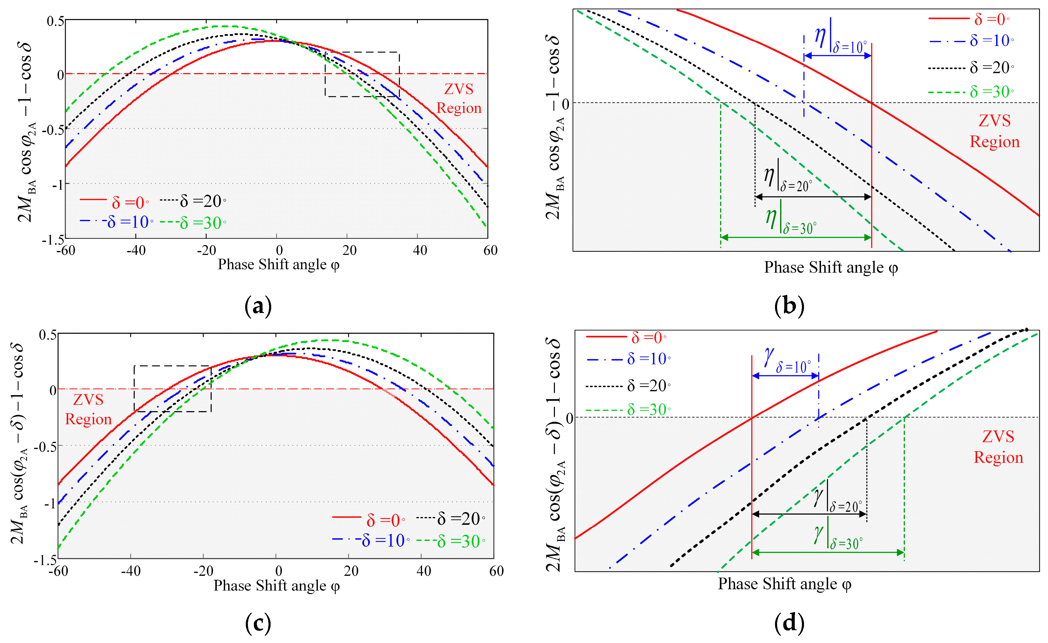
To transfer same power under traditional phase shift control method and newly proposed PWM-PHS control method, phase shift angles of φ2, φ2A and δ should satisfy the constraint condition shown in (36) and (37). The diagram of ZVS operating range of primary side phase leg A and B for the variation of δ under MBA = 1.15 is given in Figure 13:
Figure 13a,c shows the ZVS range of phase leg A and B in the primary side, Figure 13b,d is the zoom-in diagrams of Figure 13a,c, respectively. The enlarged ZVS range of phase leg A and B are defined as η and γ respectively. Figure 13 shows that the ZVS range of phase leg A and B can be enlarged with the increase of δ. The enlarged ZVS range of phase leg A and B are represented in Figure 13b,d. During η and γ, the ZVS MOSFETs number of primary side under traditional phase shift control (δ = 0) is 0, while the ZVS MOSFETs number under PWM-PHS control (δ ≠ 0) is 2.
The theoretical analysis results prove that the proposed PWM-PHS control method can increase the number of MOSFETs which can realize ZVS under specific power condition.
4.3. Control Strategy of the Proposed Two-Stage Three-Port BDC
Through the proposed two-stage three-port BDC, HESS is integrated to the DC bus of DC microgrid. The proposed three-port BDC is composed of two parts: three-port SR BDC and three-phase interleaved BDC. The control target of three-port SR BDC is to keep DC bus voltage constant by compensating the mismatch between generation and demand. Meanwhile, the control objective of the three-phase interleaved BDC is converting the widely fluctuating SC voltage Vsc to a constant voltage Vdc-link. The control scheme for the proposed two-stage three-port BDC is shown in Figure 14.
The basic idea of the three-port SR BDC is that the battery supports slow transients, and SC supports fast transients. The control structure has an inner current loop as well as an outer control loop for voltage stabilization. The bus voltage Vbus is compared with the reference voltage Vbus*, and the deviation of voltage is tracked by the voltage PI controller to produce the total current reference ibus*. By using a low-pass filter (LPF), the total current is divided into a dynamic component ibus_SC* and an average component ibus_BA*. Then, the reference currents of SC and BA are derived as iP1* and iP2* respectively. Through the inner current loops, phase shift angles are adjusted to maintain a constant DC bus voltage.
The control objective of the three-phase interleaved BDC is to keep the dc-link voltage constant. Same with the control method of three-port SR BDC, Vdc-link is compared with reference voltage Vdc-link*. The current reference is obtained through the outer voltage loop. Combining the current reference and voltage values, the driving frequency f and duty ratio D are deduced. Through the interleaved PWM generator, driving signals of three-phase interleaved BDC are acquired.
5. Experimental Results
To verify the validity of theoretical analyses, a 1 kW prototype was built in the laboratory. The MOSFETs adopted in the system are C3M0065090D units from CREE (Durham, NC, USA). The control platform is a TMS320F28379D from Texas Instruments (Dallas, TX, USA). Based on the theoretical analysis above, a set of optimized parameters of the proposed system are selected and shown in Table 1.
5.1. SC and BA Charging Mode
For the SC and BA charging mode, a 200 V voltage source is provided for port 3, port 1 and port 2 are connected to resistive loads of 15 Ω, in this experiment VT1 and VT2 lag VT3. Port 1 and 2 are entirely independent from each other. The concrete data of this experiment are as follows: input voltage Vbus = 200 V, output voltage Vdc-link = 84 V, driving frequency fs = 130 kHz, φ1 = −18.5°, φ2 = −20°; VBA = 102 V, P1 = −458.2 W, P2 = −684.5 W, P3 = −1204.3 W. The efficiency is 94.9%. MSC = MBA = 1, thus all switches of 3 ports can realize ZVS. The required phase shift angles to realize MSC = MBA = 1 are compared in Table 2. It is proved that the experimental results are consistent with theoretical analysis.
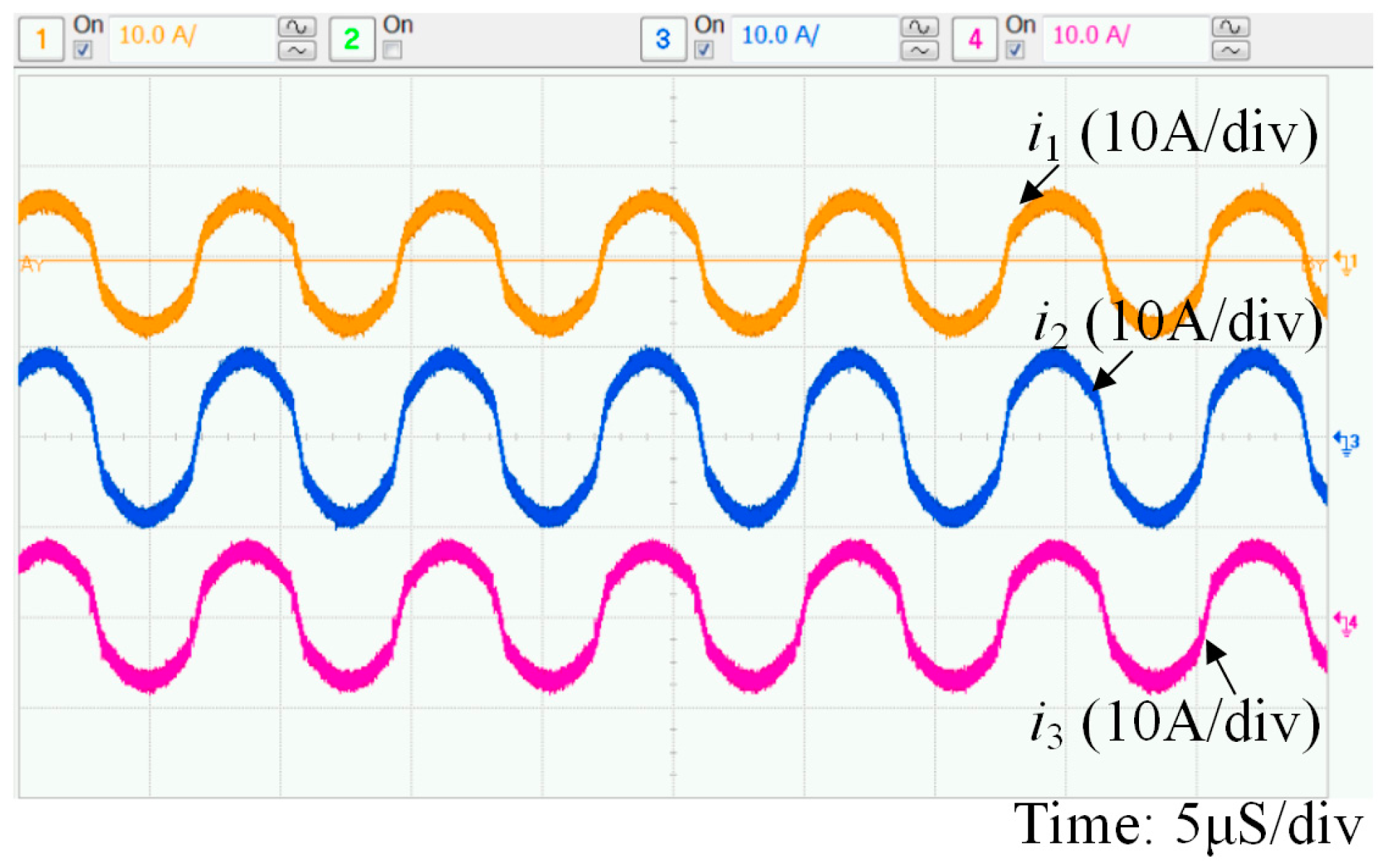
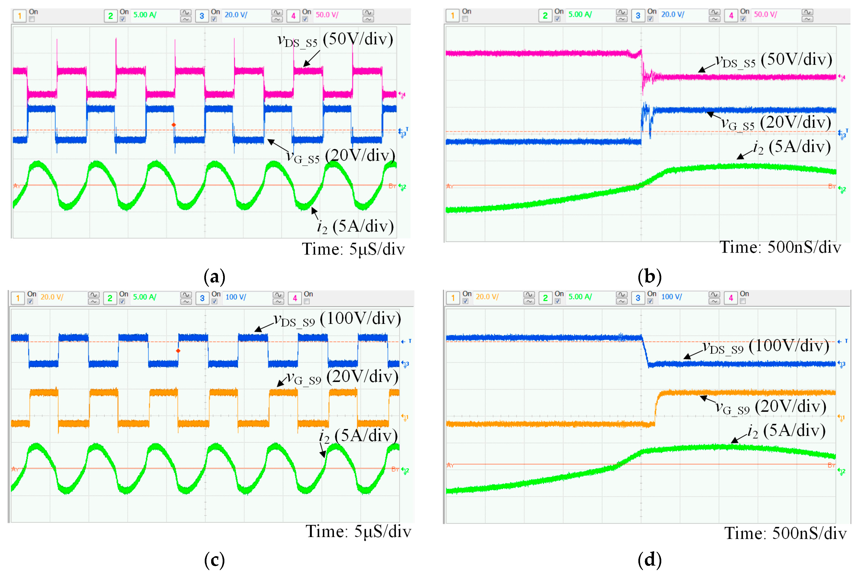
Figure 15 shows the waveforms of resonant currents of the three-port SR BDC.
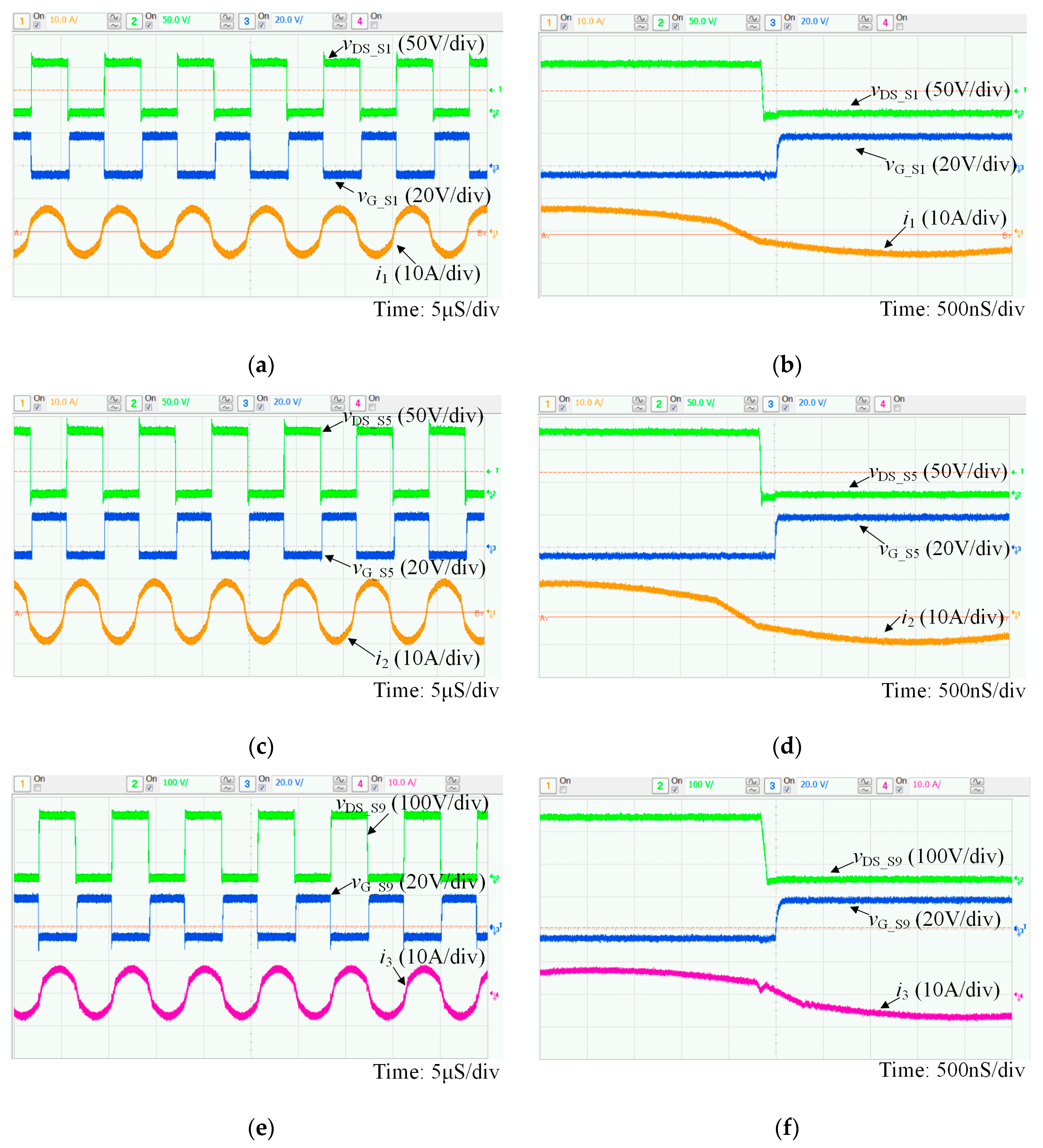
Figure 16 shows the waveforms of resonant currents and transformer voltages of three ports. Figure 16a,b show the operating waveforms of port 1, such as resonant current i1, drain-source voltage and driving voltage of S1 vDS_S1 and vG_S1. Figure 16b is the zoom-in waveforms of Figure 16a, from it we can see that the MOSFETs of port 1 can realize ZVS. Figure 16c,d show the operating waveforms of port 2, resonant current i2, drain-source voltage and driving voltage of S5 vDS_S5 and vG_S5. Figure 16e,f show waveforms of port 3. It is shown that MOSFETs of port 2 and 3 can realize ZVS under SC and BA charging mode with MSC = MBA = 1.
5.2. SC and BA Discharging Mode
In the SC and BA discharging mode, two voltage sources are connected to SC and BA port respectively, a resistive load of 40 Ω is connected to port 3. Power is transferred from port 1 and 2 to port 3. Both MbusSC and MbusBA are designed as 0.5. The concrete data of this experiment are as follows: input voltage VSC = 30 V, VBA = 102 V, Vdc-link = 85 V, output voltage Vbus = 200 V; driving frequency fs = 130 kHz, φ1 = 18.2°, φ2 = 13.4°; P1 = 521.5 W, P2 = 533.9 W, P3 = 993.1 W. The efficiency of two stage three-port BDC is 94.1%. All switches of three ports can realize ZVS.
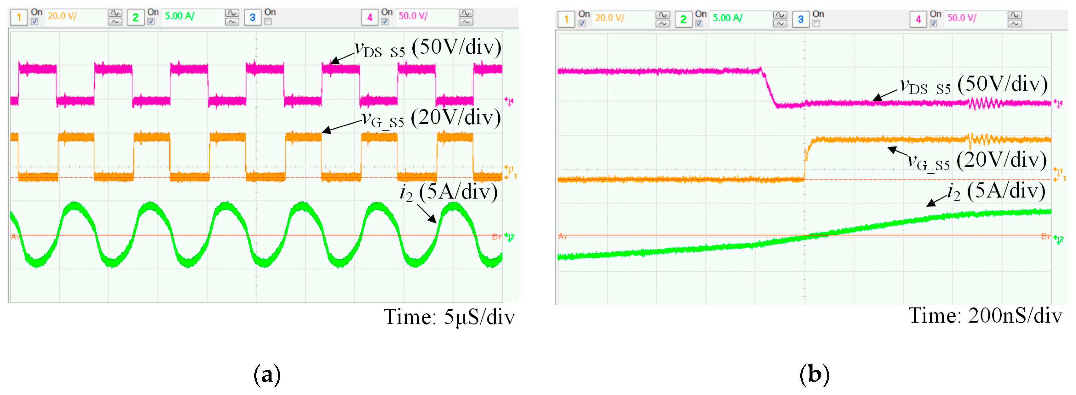
The required phase shift angles to realize MbusBA = MbusSC = 0.5 are compared in Table 3. It is proved that the experimental results are consistent with theoretical analysis. For the three-phase interleaved BDC, inductor currents iL1–iL3 and Vdc-link are shown in Figure 17, and they are completely consistent with the theoretical analysis waveforms.
Figure 18 shows the waveforms of resonant currents of three ports. Figure 19a shows i1, vDS_S1 and vG_S1 of port 1. Figure 19c shows i2, vDS_S5 and vG_S5 of port 2. Figure 19e shows i3, vDS_S9 and vG_S9 of port 3. Figure 19b,d,f is enlarged waveforms of Figure 19a,c,e. The waveforms of three ports are consistent with analysis above, and all MOSFETs of three-ports can realize under conditions when MSC = MBA = 1.
5.3. Proposed PWM-PHS Control Method
The effectiveness of proposed PWM-PHS control method is verified based on the BA channel for battery discharging mode. A 80 Ω resistive load is connected to port 3. The operating parameters are defined as follows: VBA = 45 V, Vbus = 100 V, MBA = 1.15. Two groups of contrast experiment are done, two groups adapt traditional phase-shift and the newly proposed PWM-PHS control method, respectively.
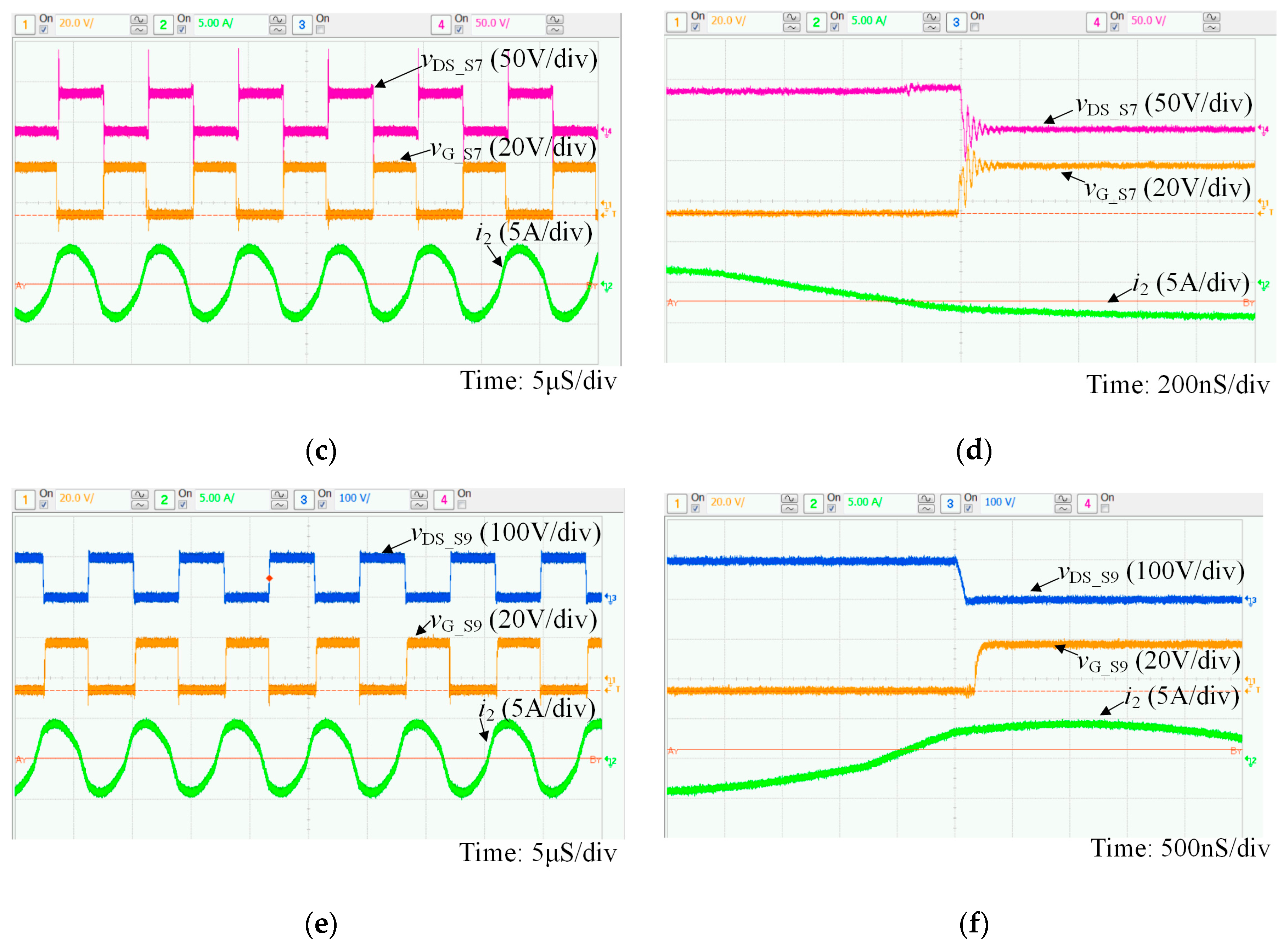
The operating parameters under traditional phase shift control method are as follows: driving frequency fs = 130 kHz, φ2A = φ2B = 23.4°, P2 = 138.3 W, P3 = 124.6 W, the efficiency is 90.1%. Figure 20a,c shows the operating waveforms of port 2 and 3. Resonant current i2, drain-source voltage and driving voltage of S5 and S9 are given. Figure 20b,d is enlarged waveforms of Figure 20a,c. Experimental results show that MOSFETs of BA port can’t realize ZVS, MOSFETs of DC bus port operate under ZVS when MBA = 1.15.
As shown in Figure 20a,b, MOSFETs of BA port can’t realize ZVS, drive signal of S5 turns positive before the output capacitor of S5 gets fully discharged. Parasitic ringing, which is due to oscillation between output capacitance of S5 and parasitic inductance present in the converter layout, occurs during turn-on switching transient. In Figure 20c,d, output capacitor is fully discharged before driving signal turns positive. Consequently, ZVS is achieved for MOSFETs of DC bus port, and parasitic ringing is avoided.
The operating parameters under phase shift control method are as follows: driving frequency fs = 130 kHz, φ2A =35.8°, φ2B = 10.8°, P2 = 134.8 W, P3 = 125 W, the efficiency is 92.7%. The efficiency is relatively low since the power level is low.
Figure 21a,c shows the operating waveforms of phase leg A and B of port 2 respectively. Figure 21e shows waveforms of port 3. Resonant current i2, drain-source voltage and driving voltage of S5, S7 and S9 are given. Figure 21b,d,f is enlarged waveforms of Figure 21a,c,e. Experimental results show that MOSFETs of phase A of BA port realize ZVS, MOSFETs of phase B of BA port can’t realize ZVS, MOSFETs of DC bus port achieve ZVS operating when MBA = 1.15.
Like the conditions shown in Figure 20a,b, MOSFETs of phase B can’t realize ZVS, and parasitic ringing presents during the turn-on switching transients. The experimental results above show that, when using traditional phase shift control method, only four switches can realize ZVS, and the efficiency is 90.1%. While, by adopting the newly proposed, the number of switches which can realize ZVS increases to 6, and the efficiency increases to 92.7%. The experimental results are consistent with theoretical analysis. It is proved that the PWM-PHS control method can improve operating characteristics of SR BDC under the condition of MBA > 1.
6. Conclusions
In this paper, a two-stage three-port BDC is fabricated to interface SC and BA with the DC microgrid. It is composed of a three-port SR BDC and a three-phase interleaved BDC. The particular two-stage structure makes it possible to handle wide voltage variations at SC port, and will ensure unity voltage gain between SC and DC bus ports. In addition, a PWM-PHS hybrid control method is applied on the BA channel. The proposed control method contributes to an increasing number of switches operating under ZVS under variable voltage gain. Together with the proposed PWM-PHS control strategy, the proposed BDC acquires optimized operation characteristics with both enlarged ZVS range and reduced power circulation loss. Finally, a 1 kW prototype is built, and the efficiency of SC and BA charging and discharging mode are 94.9% and 94.1% respectively. The experimental results validate that all switches of SC and DC bus ports can realize ZVS under varying VSC. With the proposed topology and PWM-PHS control method, two more switches of BA port achieve ZVS even under the worst input condition of MBA = 1.15.
Acknowledgments
This research was supported by the National High Technology Research and Development Program of China (863 Program) (Grant: 2015AA050603) and supported by Tianjin Municipal Science and Technology Commission (Grant: 14ZCZDGX00035). The authors would also like to thank the anonymous reviewers for their valuable comments and suggestions to improve the quality of the paper.
Author Contributions
Cheng-Shan Wang, Wei Li and Yi-Feng Wang designed the main parts of the study, including the circuit simulation model, topology innovation and simulation development. Fu-Qiang Han and Zhun Meng helped in the hardware development and experiment. Guo-Dong Li were also responsible for writing the paper.
Conflicts of Interest
The authors declare no conflict of interest.
References
- Marzband, M.; Ardeshiri, R.R.; Moafi, M.; Uppal, H. Distributed generation for economic benefit maximization through coalition formation based on Game Theory. Int. Trans. Electr. Energy Syst. 2017, 1–16. [Google Scholar] [CrossRef]
- Han, Y.; Chen, W.; Li, Q. Energy Management Strategy Based on Multiple Operating States for a Photovoltaic/Full Cell/Energy Storage DC Microgrid. Energies 2017, 10, 136. [Google Scholar] [CrossRef]
- Liu, J.; Zhang, L. Strategy Design of Hybrid Energy Storage System for Smoothing Wind Power Fluctuations. Energies 2016, 9, 991. [Google Scholar] [CrossRef]
- Marzband, M.; Ghazimirsaeid, S.S.; Uppal, H.; Fernando, T. A real-time evaluation of energy management systems for smart hybrid home Microgrids. Electr. Power Syst. Res. 2017, 143, 624–633. [Google Scholar] [CrossRef]
- Marzband, M.; Moghaddam, M.M.; Akorede, M.F.; Khomeyrani, G. Adaptive load shedding scheme for frequency stability enhancement in microgrids. Electr. Power Syst. Res. 2016, 140, 78–86. [Google Scholar] [CrossRef]
- Xu, Q.; Hu, X.; Wang, P.; Xiao, J.; Tu, P.; Wen, C.; Lee, M.Y. A Decentralized Dynamic Power Sharing Strategy for Hybrid Energy Storage System in Autonomous DC Microgrid. IEEE Trans. Ind. Electr. 2016. [Google Scholar] [CrossRef]
- Kollimalla, S.K.; Mishra, M.K.; Ukil, A.; Gooi, H.B. DC Grid Voltage Regulation Using New HESS Control Strategy. IEEE Trans. Sustain. Energy 2016, 8, 772–781. [Google Scholar] [CrossRef]
- Jin, Z.; Hou, M.; Dong, F.; Li, Y. A New Control Strategy of DC Microgrid with Photovoltaic Generation and Hybrid Energy Storage. In Proceedings of the IEEE PES Asia-Pacific Power and Energy Conference, Xi’an, China, 25–28 October 2016; pp. 434–438. [Google Scholar]
- Marzband, M.; Alavi, H.; Ghazimirsaeid, S.S.; Uppal, H.; Fernando, T. Optimal Energy Management System Based on Stochastic Approach for a Home Microgrid with Integrated Responsive Load Demand and Energy Storage. Sustain. Cities Soc. 2017, 28, 256–264. [Google Scholar] [CrossRef]
- Marzband, M.; Parhizi, N.; Savaghebi, M.; Guerrero, J.M. Distributed Smart Decision-Making for a Multi-microgrid System Based on a Hierarchical Interactive Architecture. IEEE Trans. Energy Convers. 2016, 31, 637–648. [Google Scholar] [CrossRef]
- Marzband, M.; Azarinejadian, F.; Savaghebi, M.; Guerrero, M. An Optimal Energy Management System for Islanded Microgrids Based on Multiperiod Artificial Bee Colony Combined With Markov Chain. IEEE Syst. J. 2015, 100, 1–11. [Google Scholar] [CrossRef]
- Marzband, M.; Yousefnejad, E.; Sumper, A.; Domínguez-García, J.L. Real Time Experimental Implementation of Optimum Energy Management System in Standalone Microgrid by Using Multi-layer Ant Colony Optimization. Int. Trans. Electr. Energy Syst. 2016, 75, 265–274. [Google Scholar] [CrossRef]
- Marzband, M.; Ghadimi, M.; Sumper, A.; Domínguez-García, J.L. Experimental validation of a real-time energy management system using multi-period gravitational search algorithm for microgrids in islanded mode. Appl. Energy 2014, 128, 164–174. [Google Scholar] [CrossRef]
- Marzband, M.; Parhizi, N.; Adabi, J. Optimal energy management for stand-alone microgrids based on multi-period imperialist competition algorithm considering uncertainties: Experimental validation. Int. Trans. Electr. Energy Syst. 2016, 26, 1358–1372. [Google Scholar] [CrossRef]
- Marzband, M.; Sumper, A.; Ruiz-Álvarez, A.; Domínguez-García, J.L. Experimental evaluation of a real time energy management system for stand-alone microgrids in dayahead markets. Appl. Energy 2013, 106, 365–376. [Google Scholar] [CrossRef]
- Marzband, M.; Sumper, A.; Domínguez-García, J.L.; Gumara-Ferret, R. Experimental Validation of a Real Time Energy Management System for Microgrids in Islanded Mode Using a Local Day-Ahead Electricity Market and MINLP. Energy Convers. Manag. 2013, 76, 314–322. [Google Scholar] [CrossRef]
- Zhang, N.; Sutanto, D.; Muttaqi, K.M. A review of topologies of three-port DC–DC converters for the integration of renewable energy and energy storage system. Renew. Sustain. Energy Rev. 2016, 56, 388–401. [Google Scholar] [CrossRef]
- Chien, L.J.; Chen, C.C.; Chen, J.F.; Hsieh, Y.P. Novel Three-Port Converter with High-Voltage Gain. IEEE Trans. Power Electron. 2014, 29, 4693–4703. [Google Scholar] [CrossRef]
- Lai, C.M.; Yang, M.J. A High-Gain Three-Port Power Converter with Fuel Cell, Battery Sources and Stacked Output for Hybrid Electric Vehicles and DC-Microgrids. Energies 2016, 9, 180. [Google Scholar] [CrossRef]
- Hu, Y.; Xiao, W.; Cao, W.; Ji, B. Three-Port DC–DC Converter for Stand-Alone Photovoltaic Systems. IEEE Trans. Power Electron. 2015, 30, 3068–3076. [Google Scholar] [CrossRef]
- Wang, Z.; Li, H. An Integrated Three-Port Bidirectional DC-DC Converter for PV Application on a DC Distribution System. IEEE Trans. Power Electron. 2013, 28, 4612–4624. [Google Scholar] [CrossRef]
- Sun, X.; Shen, Y.; Li, W. A Novel LLC Integrated Three-port DC-DC Converter for Stand-alone PV/Battery System. In Proceedings of the IEEE Transportation Electrification Conference and Expo, Asia-Pacific, Beijing, China, 31 August–3 September 2014; pp. 1–6. [Google Scholar]
- Duarte, J.L.; Hendrix, M.; Simões, M.G. Three-Port Bidirectional Converter for Hybrid Fuel Cell Systems. IEEE Trans. Power Electron. 2007, 22, 480–487. [Google Scholar] [CrossRef]
- Phattanasak, M.; Gavagsaz-Ghoachani, R.; Martin, J.P.; Pierfederici, S. Flatness Based control of an Isolated Three-port Bidirectional DC-DC converter for a Fuel cell hybrid source. In Proceedings of the IEEE Energy Conversion Congress and Exposition, Phoenix, AZ, USA, 17–22 September 2011; pp. 977–984. [Google Scholar]
- Fontana, C.; Buja, G.; Bertoluzzo, M.; Kumar, K. Power and control characteristics of an isolated three-port DC-DC converter under DCM operations. In Proceedings of the Annual Conference of the IEEE Industrial Electronics Society, Florence, Italy, 24–27 October 2016; pp. 4211–4216. [Google Scholar]
- Phattanasak, M.; Gavagsaz-Ghoachani, R.; Martin, J.P.; Nahid-Mobarakeh, B. Control of a Hybrid Energy Source Comprising a Fuel Cell and Two Storage Devices Using Isolated Three-Port Bidirectional DC–DC Converters. IEEE Trans. Ind. Appl. 2015, 51, 491–497. [Google Scholar] [CrossRef]
- Wang, L.; Wang, Z.; Li, H. Asymmetrical Duty Cycle Control and Decoupled Power Flow Design of a Three-port Bidirectional DC-DC Converter for Fuel Cell Vehicle Application. IEEE Trans. Power Electron. 2012, 27, 891–904. [Google Scholar] [CrossRef]
- Wang, Z.; Liu, B.; Zhang, Y.; Cheng, M.; Chu, K.; Xu, L. The Chaotic-Based Control of Three-Port Isolated Bidirectional DC/DC Converters for Electric and Hybrid Vehicles. Energies 2016, 9, 83. [Google Scholar] [CrossRef]
- Ling, Z.; Wang, H.; Yan, K.; Gan, J. Optimal Isolation Control of Three-Port Active Converters as a Combined Charger for Electric Vehicles. Energies 2016, 9, 715. [Google Scholar] [CrossRef]
- Li, X.; Bhat, A.K.S. Analysis and Design of High-Frequency Isolated Duan-Bridge Series Resonant DC/DC Converter. IEEE Trans. Power Electron. 2010, 25, 850–862. [Google Scholar]
- Krishnaswami, H.; Mohan, N. Three-Port Series-Resonant DC-DC Converter to Interface Renewable Energy Sources with Bidirectional Load and Energy Storage Ports. IEEE Trans. Power Electron. 2009, 24, 2289–2297. [Google Scholar] [CrossRef]
- Shreelekha, K.; Arulmozhi, S. Multiport isolated bidirectional DC-DC converter interfacing battery and supercapacitor for hybrid energy storage application. In Proceedings of the International Conference on Electrical, Electronics, and Optimization Techiniques, Chennai, India, 3–5 March 2016; pp. 2763–2768. [Google Scholar]
- Tao, H.; Kotsopoulos, A.; Duarte, J.L.; Hendrix, M.A.M. Transformer-Coupled Multiport ZVS Bidirectional DC–DC Converter with Wide Input Range. IEEE Trans. Power Electron. 2008, 23, 771–781. [Google Scholar] [CrossRef]
- Oggier, G.; Garcia, G.O.; Oliva, A. Switching Control Strategy to Minimize Dual Active Bridge Converter Losses. IEEE Trans. Power Electron. 2009, 24, 1826–1838. [Google Scholar] [CrossRef]
- Xu, D.; Zhao, C.; Fan, H. A PWM Plus Phase-Shift Control Bidirectional DC-DC Converter. IEEE Trans. Power Electron. 2004, 19, 666–675. [Google Scholar] [CrossRef]
- Tao, H.; Duarte, J.L.; Hendrix, M.A.M. Three-Port Triple-Half-Bridge Bidirectional Converter with Zero-Voltage Switching. IEEE Trans. Power Electron. 2008, 23, 782–792. [Google Scholar]
- Baek, J.-B.; Choi, W.-I.; Cho, B.-H. Digital Adaptive Frequency Modulation for Bidirectional DC-DC Converter. IEEE Trans. Power Electron. 2013, 60, 5167–5176. [Google Scholar] [CrossRef]
- Nandankar, P.V.; Rothe, J. Hihgly efficient discontinuous mode interleaved DC-DC converter. In Proceedings of the International Conference on Electrical, Electronics, and Optimization Techiniques, Chennai, India, 3–5 March 2016; pp. 476–481. [Google Scholar]
Figure 1.
Typical structure of three-port converter: (a) non-isolated; (b) partly-isolated; (c) isolated.
Figure 1.
Typical structure of three-port converter: (a) non-isolated; (b) partly-isolated; (c) isolated.

Figure 2.
Topology of the isolated three-port BDC based on transformer and inductor.
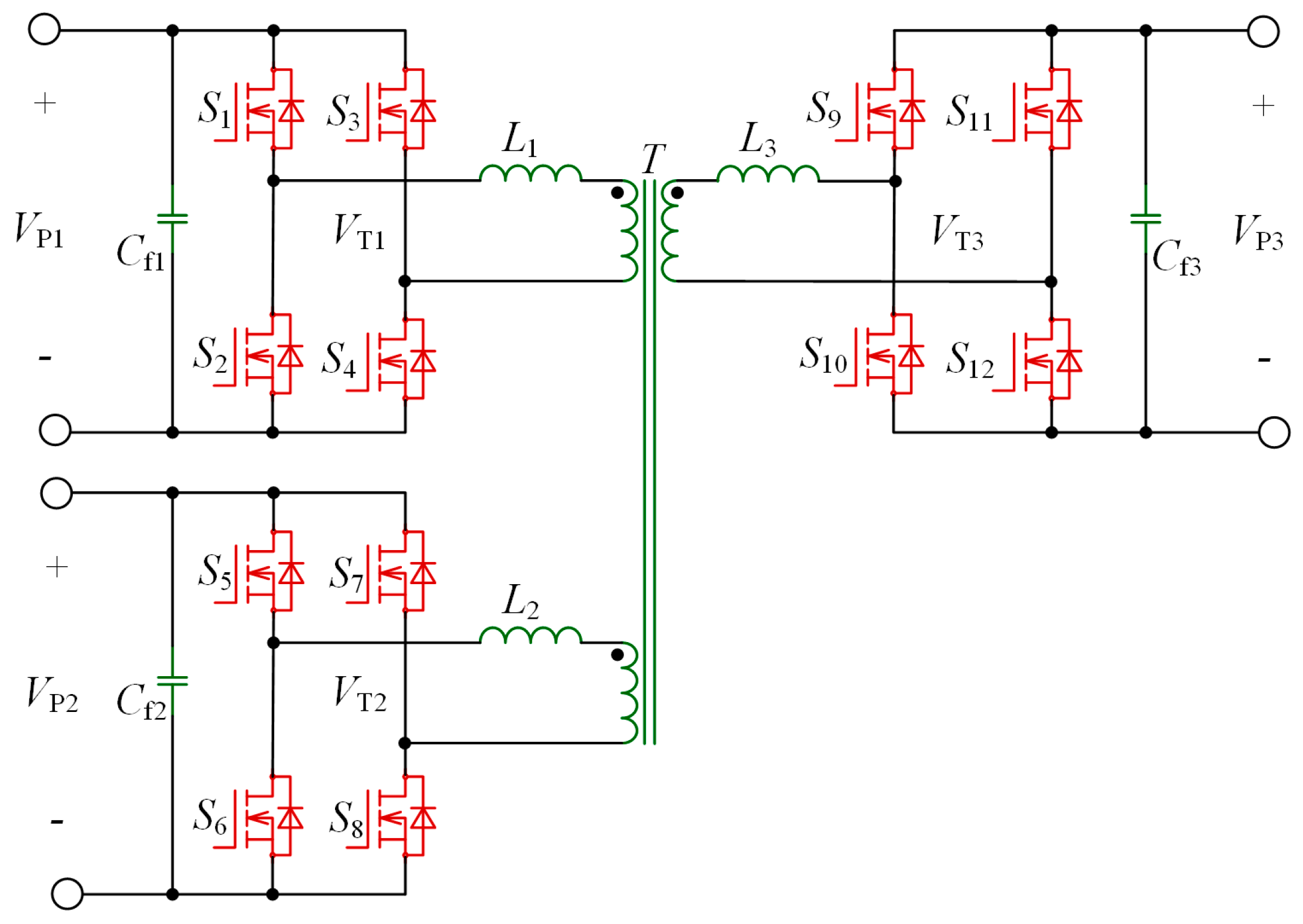
Figure 3.
Topology of the proposed HESS bidirectional DC/DC system.
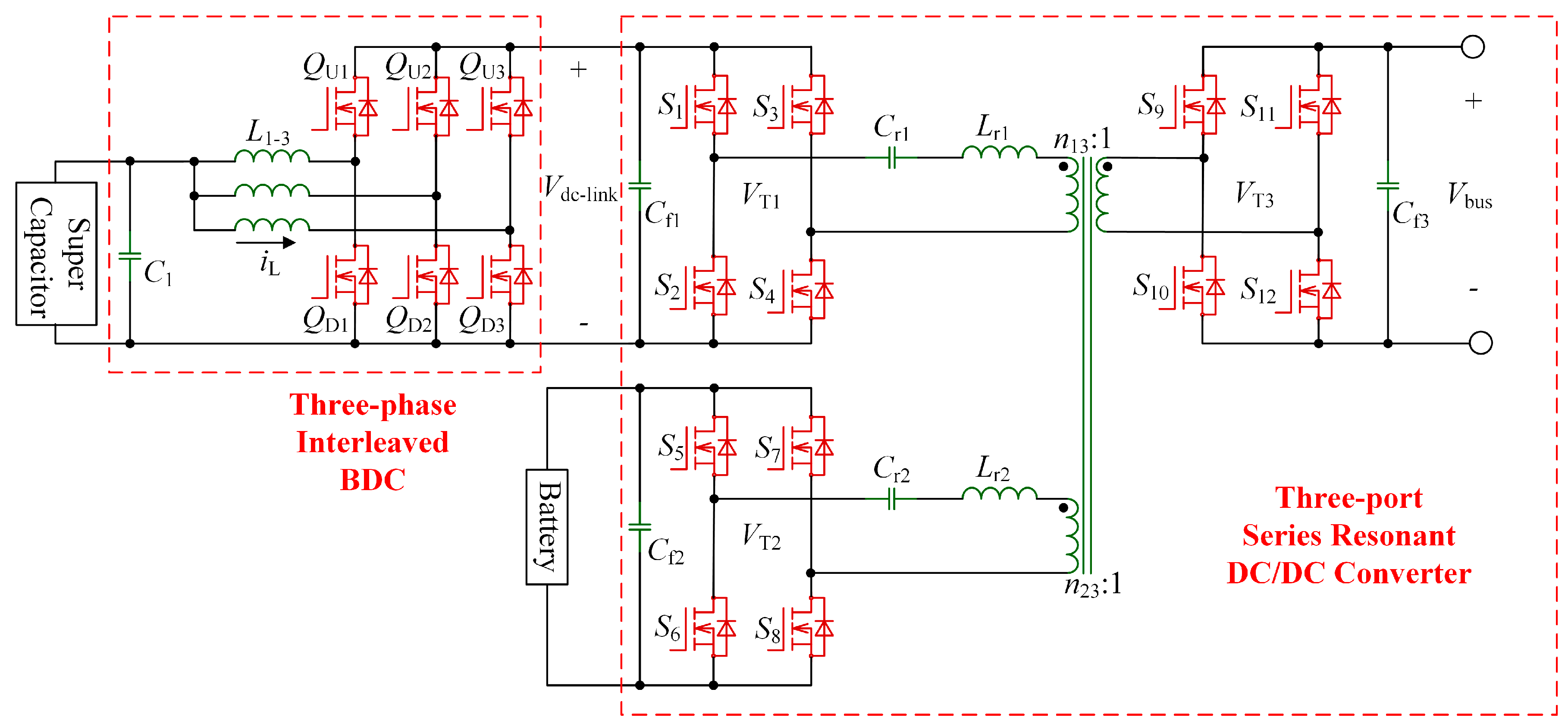
Figure 4.
Structure of the three-port SR BDC.

Figure 5.
Theoretical waveforms of the three-port SR BDC.
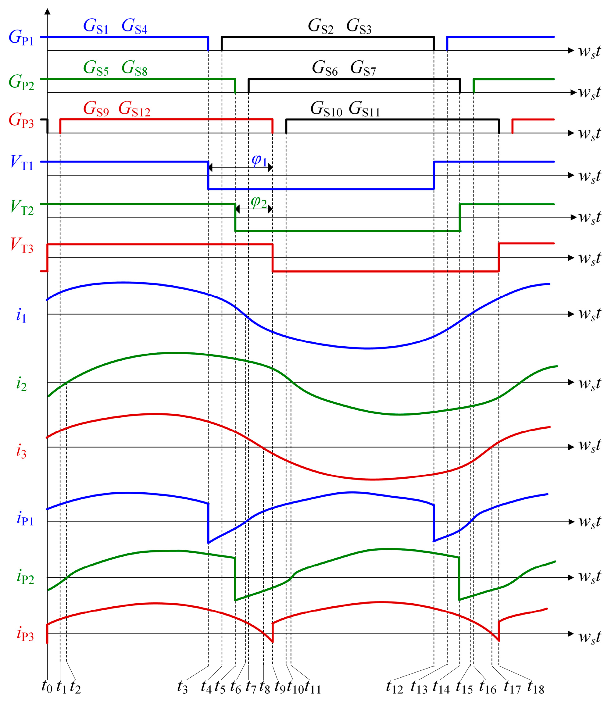
Figure 6.
Equivalent circuits for analysis: (a) equivalent circuit of three-port SR BDC; (b) transformer equivalent model.
Figure 6.
Equivalent circuits for analysis: (a) equivalent circuit of three-port SR BDC; (b) transformer equivalent model.

Figure 7.
Circuit diagram of the proposed three-phase interleaved BDC.

Figure 8.
Circuit diagram of single phase.

Figure 9.
Theoretical waveforms of single phase under boost mode.

Figure 10.
ZVS range of single channel SR BDC versus phase shift angel φ under different M: (a) primary side; (b) secondary side.
Figure 10.
ZVS range of single channel SR BDC versus phase shift angel φ under different M: (a) primary side; (b) secondary side.

Figure 11.
Peak current of single channel SR BDC versus phase shift angel φ under different M: (a) M < 1; (b) M > 1.
Figure 11.
Peak current of single channel SR BDC versus phase shift angel φ under different M: (a) M < 1; (b) M > 1.

Figure 12.
Theoretical waveforms for BA channel under PWM-PHS control method with MBA = 1.15.
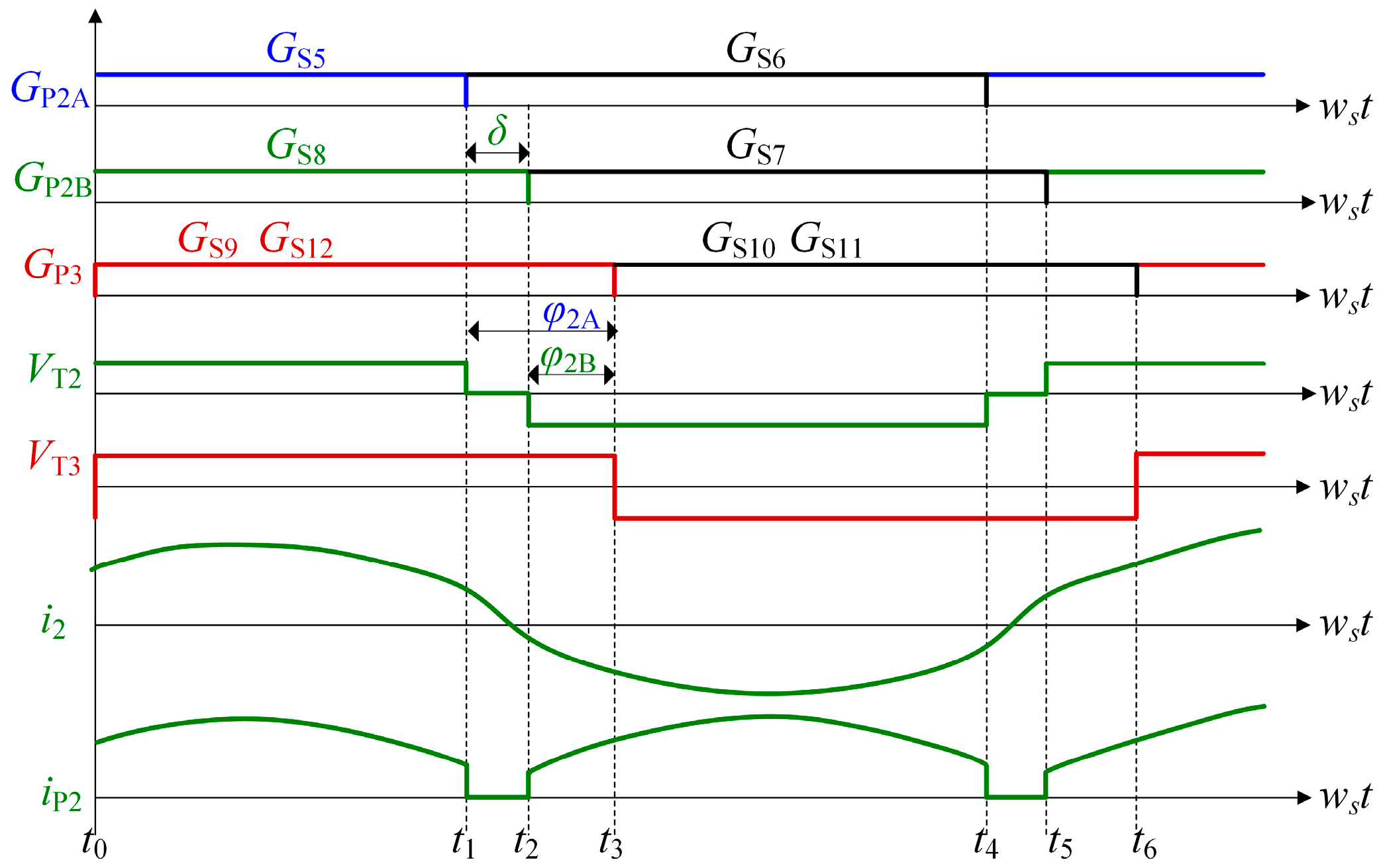
Figure 13.
Soft switching range of primary side for variation of δ under MBA = 1.15: (a) phase leg A; (b) zoom-in figure of (a); (c) phase leg B; (d) zoom-in figure of (c).
Figure 13.
Soft switching range of primary side for variation of δ under MBA = 1.15: (a) phase leg A; (b) zoom-in figure of (a); (c) phase leg B; (d) zoom-in figure of (c).

Figure 14.
Control scheme for the proposed two-stage three-port BDC.
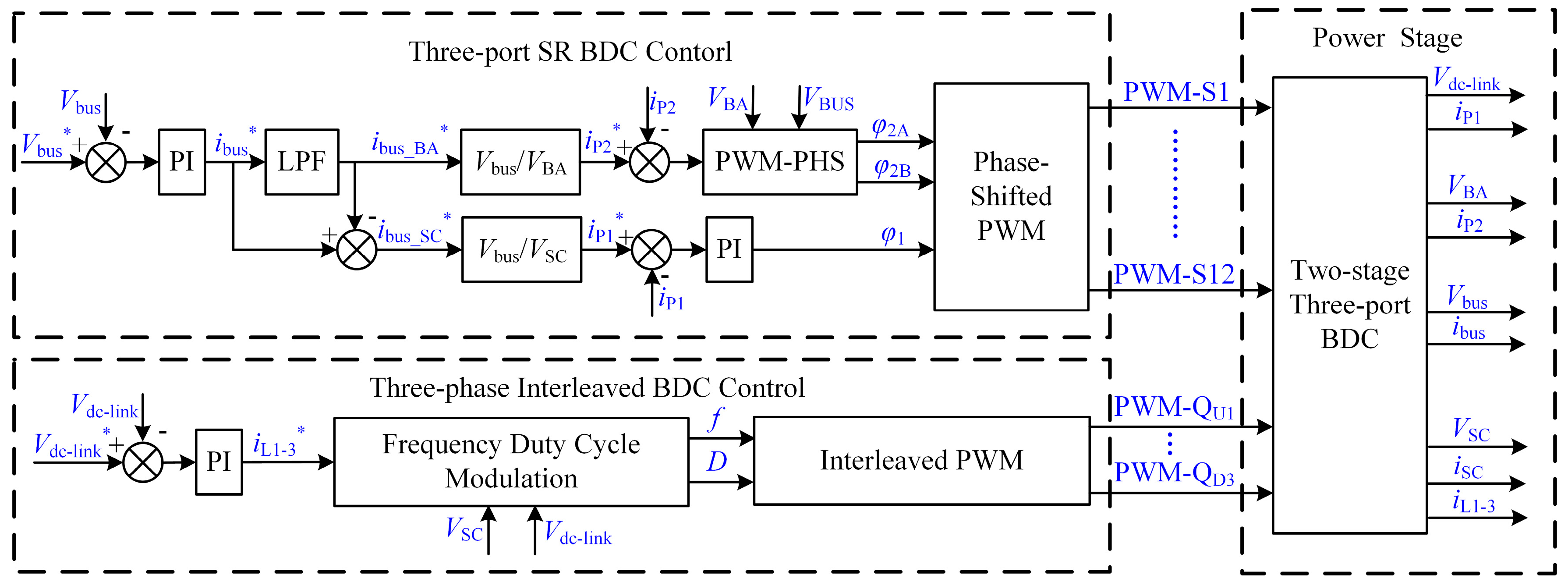
Figure 15.
Waveforms of resonant currents of three ports under SC and BA charging mode.

Figure 16.
Experimental results of three-port SR BDC under SC and BA charging mode: (a,b) SC port; (c,d) BA port; (e,f) DC bus port.
Figure 16.
Experimental results of three-port SR BDC under SC and BA charging mode: (a,b) SC port; (c,d) BA port; (e,f) DC bus port.

Figure 17.
Waveforms of three-phase interleaved BDC.
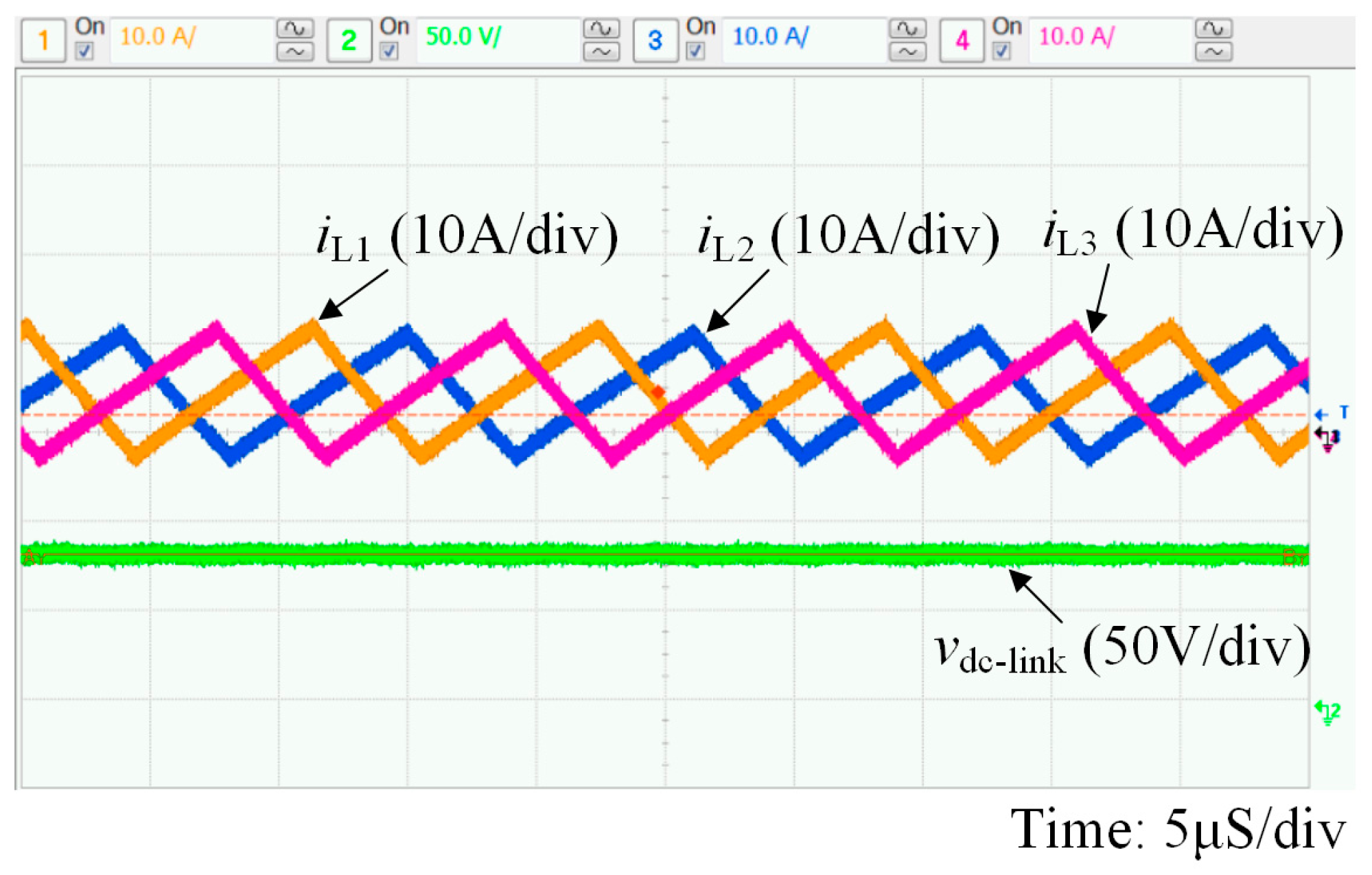
Figure 18.
Waveforms of resonant currents of three ports and transformer port voltages.
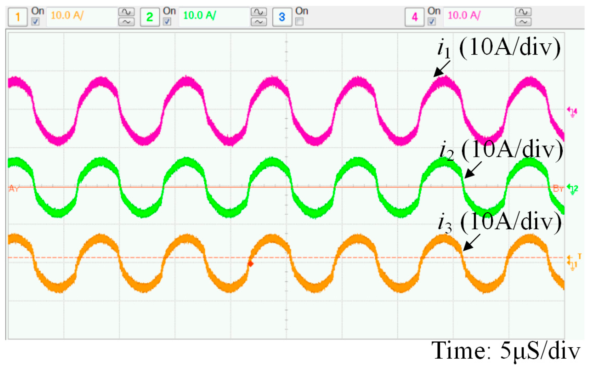
Figure 19.
Experimental results of three-port SR BDC under SC and BA charging mode: (a,b) SC port; (c,d) BA port; (e,f) DC bus port.
Figure 19.
Experimental results of three-port SR BDC under SC and BA charging mode: (a,b) SC port; (c,d) BA port; (e,f) DC bus port.
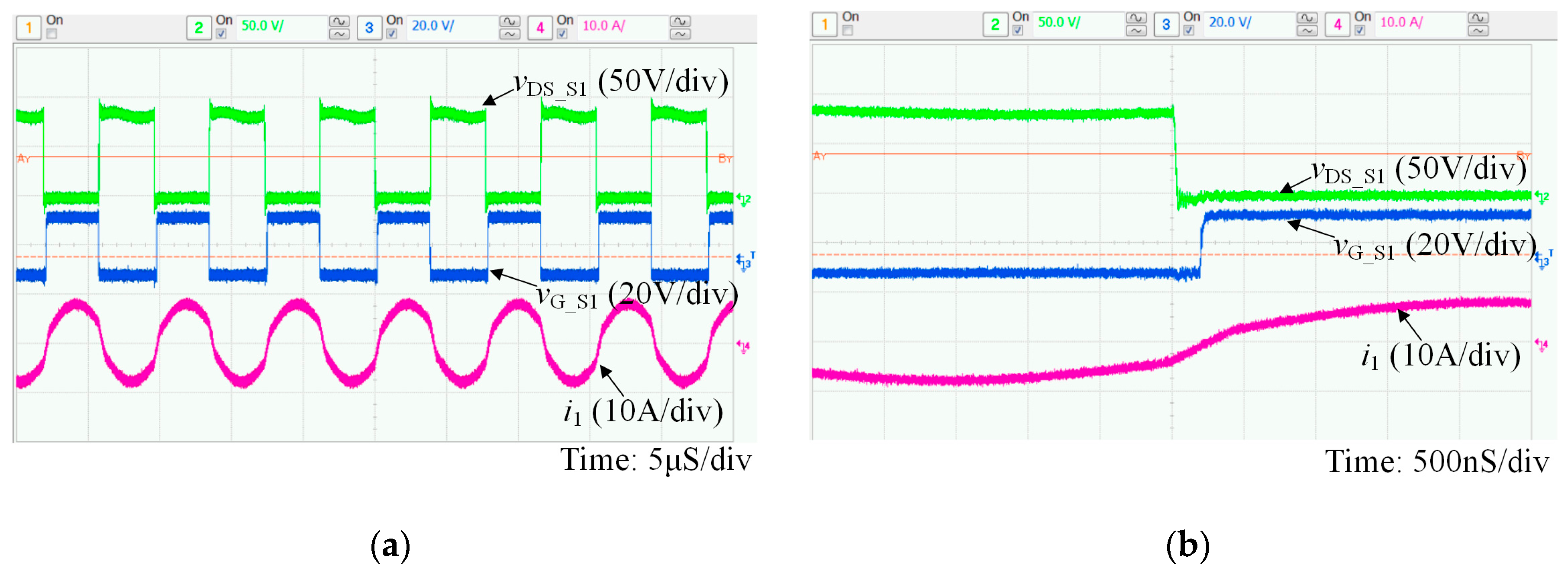
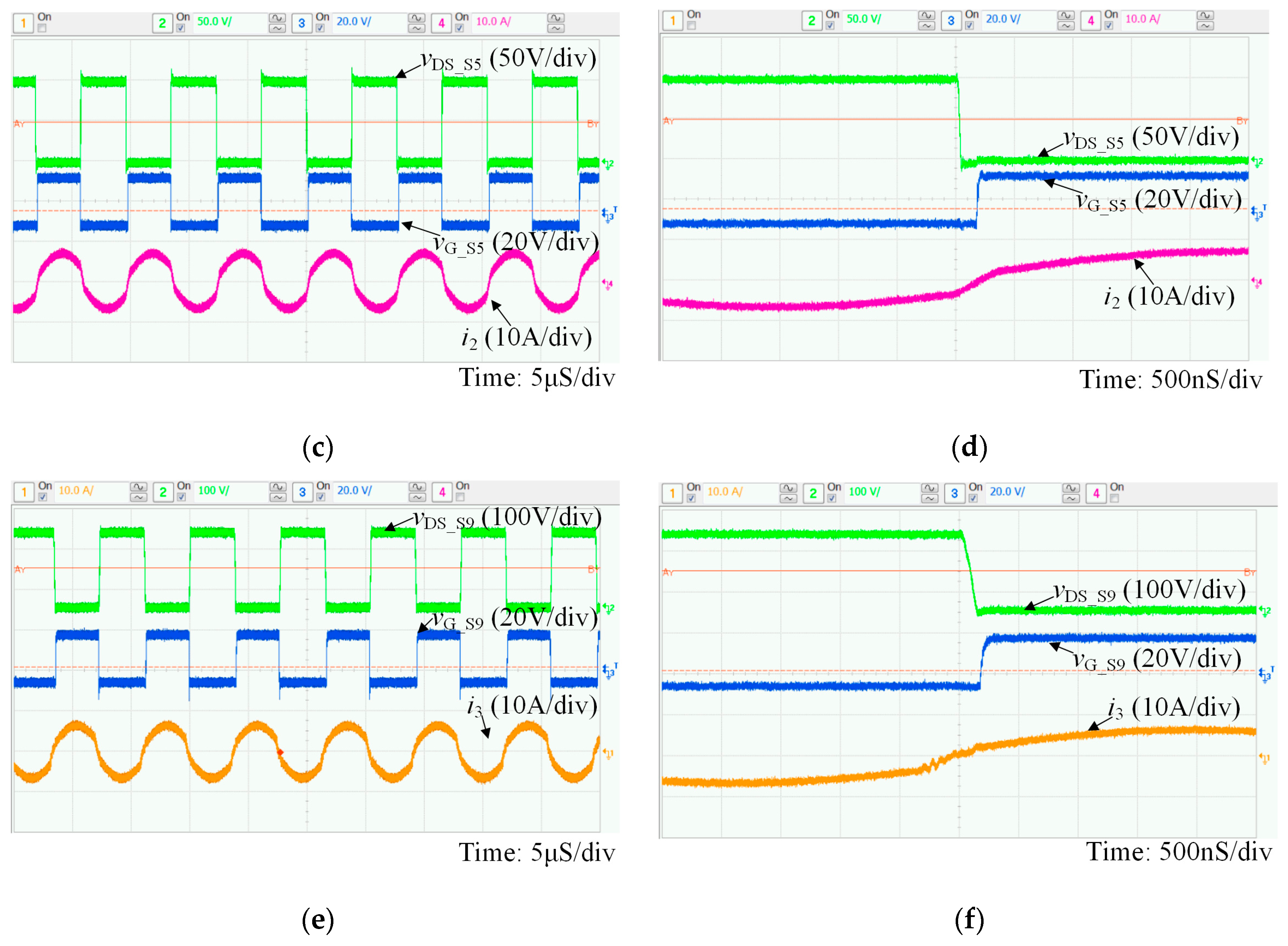
Figure 20.
Experimental results of BA channel using phase-shift control method under MBA = 1.15: (a,b) BA port; (c,d) DC bus port.
Figure 20.
Experimental results of BA channel using phase-shift control method under MBA = 1.15: (a,b) BA port; (c,d) DC bus port.

Figure 21.
Experimental results of BA channel using PWM-PHS control method under MBA = 1.15: (a,b) phase leg A of BA port; (c,d) phase leg B of BA port; (e,f) DC bus port.
Figure 21.
Experimental results of BA channel using PWM-PHS control method under MBA = 1.15: (a,b) phase leg A of BA port; (c,d) phase leg B of BA port; (e,f) DC bus port.


Table 1.
Parameters of the proposed system.
| Converter Parameter | Value |
|---|---|
| Resonant Inductor Lr1 and Lr2 | 15 μH |
| Resonant Capacitors Cr1 and Cr2 | 141 nF |
| Transformer turns ratio n13:n23:1 | 0.425:0.51:1 |
| Port 1 voltage Vdc-link | 85 V |
| Port 2 voltage VBA | 90 V–102 V |
| Port 3 voltage Vbus | 200 V |
| Voltage Gain MSC | 1 |
| Voltage Gain MBA | 1–1.15 |
| Super Capacitor Voltage VSC | 30 V–75 V |
| Buck/Boost Inductor of BDC L | 15 μH |
Table 2.
Comparison of φ1 and φ2 under theoretical calculation and experiment.
| Method | φ1 | φ2 |
|---|---|---|
| Theoretical Calculation | −19.1° | −19.1° |
| Experiment | −18.5° | −20° |
Table 3.
Comparison of φ1 and φ2 under theoretical calculation and experiment.
| Method | φ1 | φ2 |
|---|---|---|
| Theoretical Calculation | 19.8° | 13.6° |
| Experiment | 18.2° | 13.4° |
© 2017 by the authors. Licensee MDPI, Basel, Switzerland. This article is an open access article distributed under the terms and conditions of the Creative Commons Attribution (CC BY) license (http://creativecommons.org/licenses/by/4.0/).
Share and Cite
MDPI and ACS Style
Wang, C.-S.; Li, W.; Wang, Y.-F.; Han, F.-Q.; Meng, Z.; Li, G.-D. An Isolated Three-Port Bidirectional DC-DC Converter with Enlarged ZVS Region for HESS Applications in DC Microgrids. Energies 2017, 10, 446. https://doi.org/10.3390/en10040446
AMA Style
Wang C-S, Li W, Wang Y-F, Han F-Q, Meng Z, Li G-D. An Isolated Three-Port Bidirectional DC-DC Converter with Enlarged ZVS Region for HESS Applications in DC Microgrids. Energies. 2017; 10(4):446. https://doi.org/10.3390/en10040446
Chicago/Turabian StyleWang, Cheng-Shan, Wei Li, Yi-Feng Wang, Fu-Qiang Han, Zhun Meng, and Guo-Dong Li. 2017. "An Isolated Three-Port Bidirectional DC-DC Converter with Enlarged ZVS Region for HESS Applications in DC Microgrids" Energies 10, no. 4: 446. https://doi.org/10.3390/en10040446
Note that from the first issue of 2016, this journal uses article numbers instead of page numbers. See further details here.