A High-Frequency Isolation (HFI) Charging DC Port Combining a Front-End Three-Level Converter with a Back-End LLC Resonant Converter

School of Electrical Engineering, Northeast Electric Power University, Jilin 132012, China
*
Author to whom correspondence should be addressed.
Energies 2017, 10(10), 1462; https://doi.org/10.3390/en10101462
Submission received: 21 July 2017
/
Revised: 4 September 2017
/
Accepted: 11 September 2017
/
Published: 22 September 2017
(This article belongs to the Collection Electric and Hybrid Vehicles Collection)
Abstract
:The high-frequency isolation (HFI) charging DC port can serve as the interface between unipolar/bipolar DC buses and electric vehicles (EVs) through the two-power-stage system structure that combines the front-end three-level converter with the back-end logical link control (LLC) resonant converter. The DC output voltage can be maintained within the desired voltage range by the front-end converter. The electrical isolation can be realized by the back-end LLC converter, which has the bus converter function. According to the three-level topology, the low-voltage rating power devices can be adapted for half-voltage stress of the total DC grid, and the PWM phase-shift control can double the equivalent switching frequency to greatly reduce the filter volume. LLC resonant converters have advance characteristics of inverter-side zero-voltage-switching (ZVS) and rectifier-side zero-current switching (ZCS). In particular, it can achieve better performance under quasi-resonant frequency mode. Additionally, the magnetizing current can be modified following different DC output voltages, which have the self-adaptation ZVS condition for decreasing the circulating current. Here, the principles of the proposed topology are analyzed in detail, and the design conditions of the three-level output filter and high-frequency isolation transformer are explored. Finally, a 20 kW prototype with the 760 V input and 200–500 V output are designed and tested. The experimental results are demonstrated to verify the validity and performance of this charging DC port system structure.
1. Introduction
As solutions of energy crisis and environmental pollution, EVs that can run on alternative resources of energy have increasingly attracted attention for investigations of decreasing fossil fuel consumption and reducing greenhouse gas emissions [1,2]. The commercial success of EVs relies heavily on the presence of high-efficiency charging stations to increase mileage and shorten charging time [3,4,5]. Electric vehicle technologies involved with hybrid electric vehicles (HEVs), plug-in hybrid electric vehicles (PHEVs), and plug-in pure electric vehicles (PPEVs), such as the Toyota Prius and Lexus RX 400h, have been commercialized and are available in the market. A large number of high-power charging stations need to be constructed to solve consumers’ need for long-distance transport with electric vehicles (EVs). The construction of these facilities is a key factor in attracting more consumers to the use of EVs [6,7,8,9,10].
Recently, a distributed generation system, including the solar photovoltaic and wind power generation system as green energy, is playing an increasingly important role in energy structures. The combination of renewable energy sources with EV charging stations and energy storage systems is inevitable [11,12,13,14,15]. A high-efficiency, high-power-density, high-reliability, and cost-effective charging station, depicted in Figure 1, has been designed [16,17,18]. Additionally, a power electronics transformer (PET) can serve as the interface between medium- and low-voltage levels [19].
Chargers can be classified by two types—the on-board charger, located on the vehicle itself, and the off-board charger, which is distinct from the actual vehicle—each of which can be classified into three power levels reflecting charging characteristics shown in Table 1 by the Society of Automotive Engineers (SAE) [20,21,22,23]. It can be found that the on-board charger can draw AC current from any available power outlet and can efficiently charge the batteries. However, drawbacks, including a long charging time, low efficiency, and low reliability, are apparent. In addition, the on-board charger located on the vehicles can add volume and weight. Since a normal 3.3 kW charging power requires a 6–8 h charging time, most users have no choice but to recharge overnight. The off-board charger, called a fast-charger, can directly draw power from the DC bus, which can provide sufficient power for vehicles within a short period of time. For a normal 50 kW charging power, the Nissan Leaf, with its 24 kWh battery pack, takes only half an hour to recharge. The off-board charger has certain advantages compared with the on-board charger, such as a high power density and a high efficiency. The high-frequency-isolated DC-DC converters with a high power capacity are preferable to EVs’ off-board chargers in terms of satisfying the safety requirements of charging multiple EVs within an acceptable period of time [24,25,26,27,28,29,30].
In recent years, phase-shift full-bridge (PSFB) has become a popular topology for charging, but there are some obvious defects for a traditional zero-voltage-switching (ZVS) PSFB DC-DC converter. One is that ZVS cannot be achieved under light load conditions due to the limited ZVS range for lagging-leg switches. Another defect is the excessive conduction loss caused by the primary reflected current from the output inductor current [30]. The dual active bridge (DAB) converter is also a useful topology for high-power applications. It is difficult to achieve the ZVS of all active switches in the DAB converter, as the switch stress is raised in this condition. Although some switching control strategies can improve this problem, this complex modulation increases the burden for the controller and for researchers [31,32,33].
This paper proposes a high-frequency isolation (HFI) charging DC port topology. It can serve as the interface between unipolar/bipolar DC buses and electric vehicles (EVs) through the two-power-stage system structure, which combines a front-end three-level buck converter with a back-end LLC resonant converter. The DC output voltage can be regulated within the desired voltage range by the front-end three-level buck converter. Zero-voltage switching (ZVS) for the inverter side and zero-current switching (ZCS) for the rectifier side can be realized by the back-end LLC resonant converter. In Section 2, principles of the proposed charging port topology are explored in detail. In Section 3, the features and characteristics are analyzed. In Section 4, the design conditions of the three-level output filter and high-frequency isolation transformer are explored. In Section 5, a 20 kW prototype is designed and tested. The experimental results are presented to verify the validity and performance of the proposed fast-charging DC port system structure.
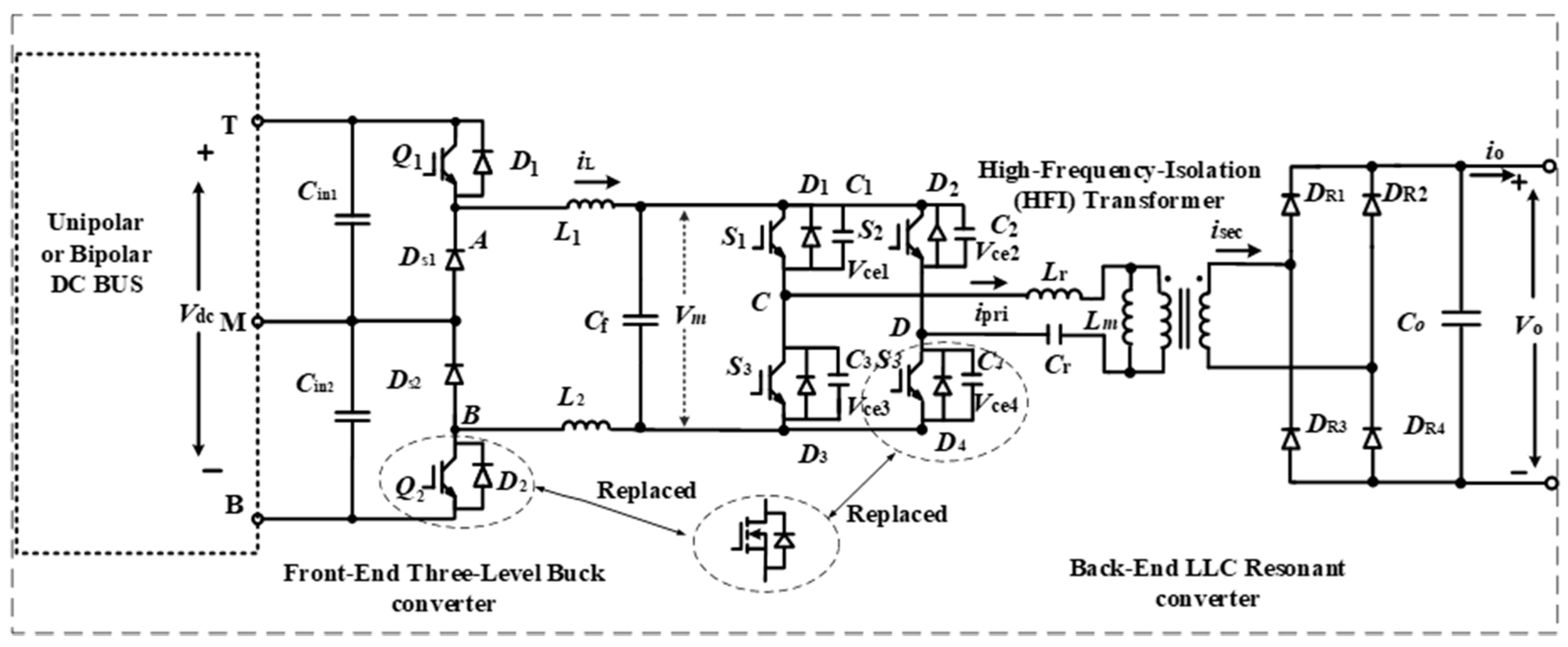
2. High-Frequency-Isolation Charging Port Topology
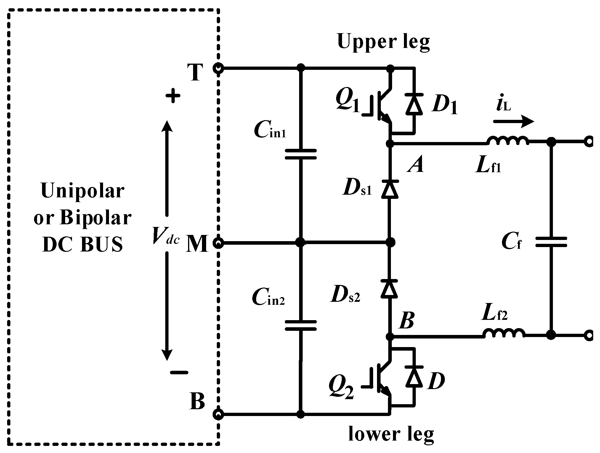
The structure of the proposed two-power-stage system for the EV’s HFI charging port is shown in Figure 2. It combines the front-end three-level buck converter, which has the ability of regulating the output DC voltage, with the back-end LLC resonant converter, which experiences high-frequency electrical isolation. Additionally, the input terminals (T, M, B) of the three-level converter can flexibly fit the bipolar DC bus or unipolar DC bus.
The main features of the system are illustrated as follows:
- (1)
- According to the three-level converter, the low-voltage level rating power switches can be adapted/selected for the half-voltage stress of total DC bus. Additionally, the proposed system structure can be practical under high-voltage and high-power conditions.
- (2)
- The PWM phase-shift control for the front-end three-level buck converter can double the equivalent switching to greatly reduce the intermediate output LC filter volume.
- (3)
- The proposed structure can regulate the DC power balance without extra balancing circuits when the input terminals (T, M, B) are interfaced with the bipolar DC bus.
- (4)
- The back-end LLC resonant converters have the advance characteristics of zero-voltage switching (ZVS) of the inverter side and zero-current switching (ZCS) of the rectifier side. In particular, it can achieve better performance under quasi-resonant frequency mode, which greatly decreases the loss of switches.
- (5)
- The magnetizing current of LLC high-frequency transformer can be automatically modified by following the different DC output voltages, which have the self-adaption ZVS condition for decreasing the circulating current.
2.1. Front-End Three-Level Buck Converter
Figure 3 shows the circuit diagram of the front-end three-level buck converter, which consists of two power switches (Q1, Q2) with the freewheeling diodes (Ds1, Ds2), the split DC-link capacitors (Cin1, Cin2), and the intermediate LC filter (Lf1, Lf2, Cf).
2.1.1. Operating Principle
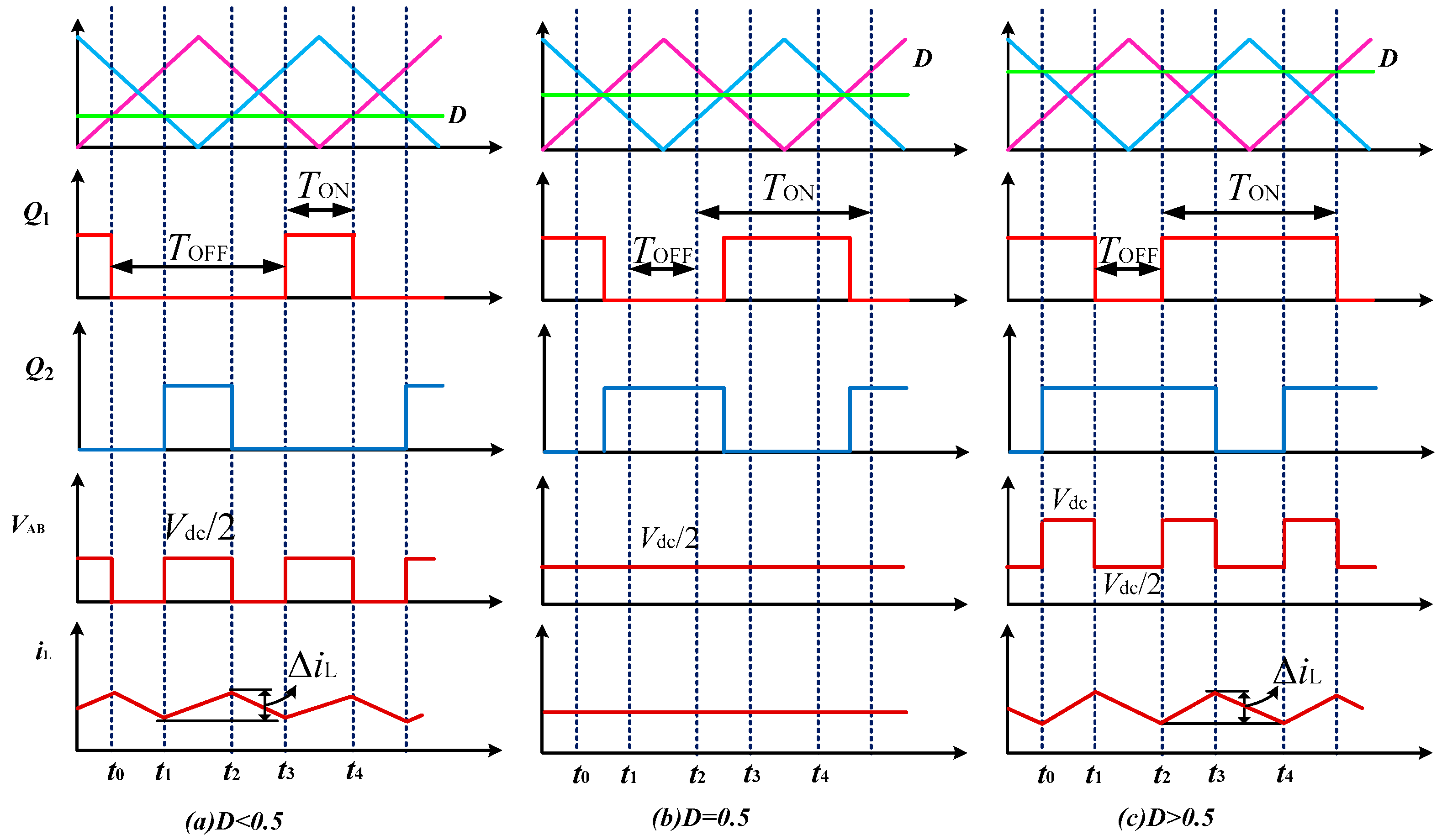
As shown in Figure 3, two switches (Q1, Q2) of the three-level buck converter are modulated by the PWM phase-shift control with the same duty cycle D. Figure 4a shows the converter operating waveforms for D < 0.5. Figure 4b shows the operating waveforms for D = 0.5, and Figure 4c shows the operating waveforms for D > 0.5. It can be found in Figure 4 that the equivalent frequency of filter inductor current iL is twice the device switching frequency. When D = 0.5, this feature can reduce the output filter volume when the current ripple ΔiL for the filter inductor is nearly zero.
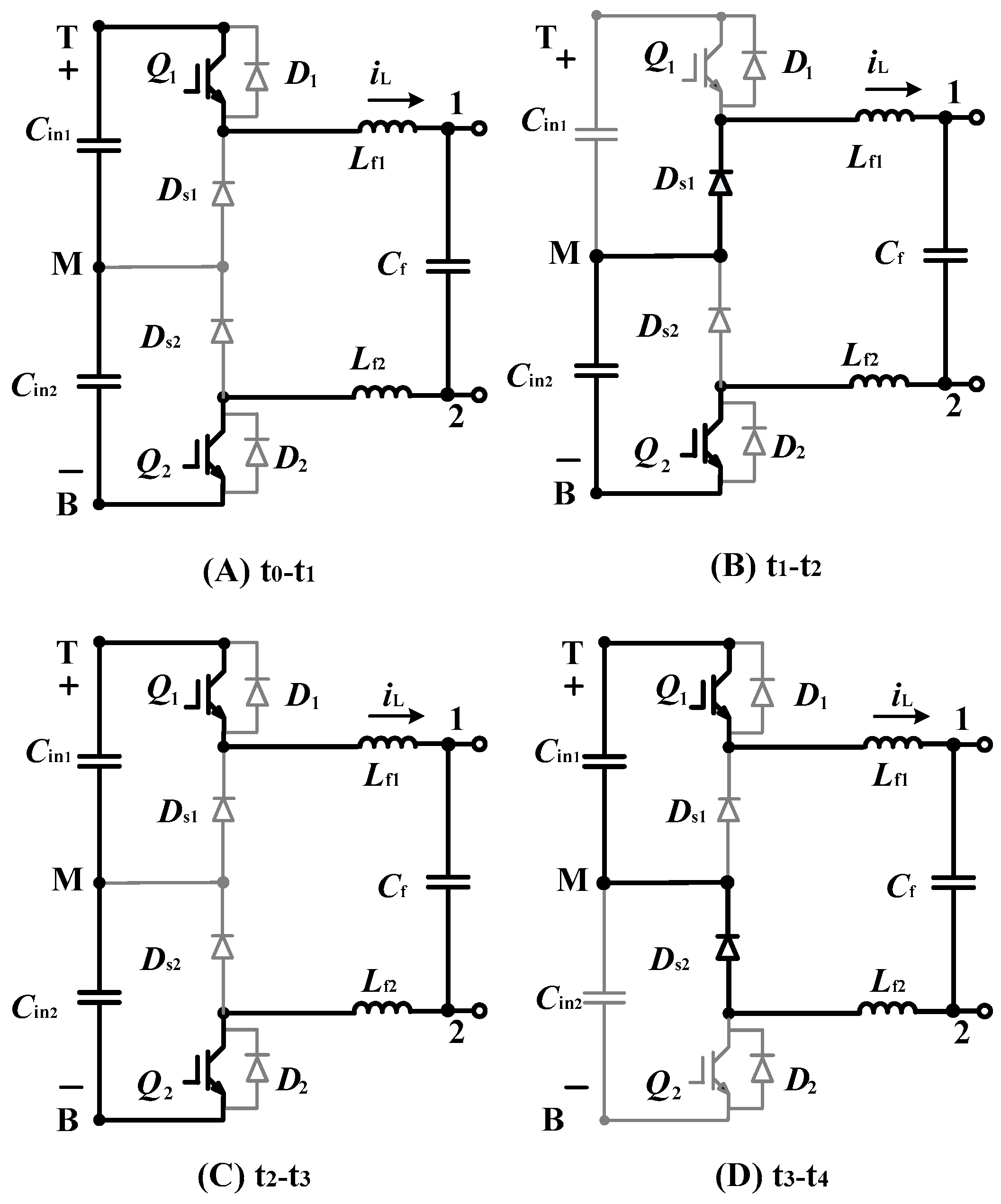
Figure 5 shows the four operating stages’ ((A) t0–t1, (B) t1–t2, (C) t2–t3, (D) t3–t4) equivalent circuits for D > 0.5. It can be found that there are three switching modes:
- Mode 1:
- When Q1 is turned on and Q2 is turned off, the generated voltage VAB is half of the DC side voltage 0.5 Vdc;
- Mode 2:
- When Q1 and Q2 are turned on at the same time, the generated voltage VAB is the total DC side voltage Vdc;
- Mode 3:
- When Q1 is tuned off and Q2 is turned on, the generated voltage VAB is half the DC side voltage 0.5 Vdc.
Figure 6 shows the equivalent circuits of two stages ((A) t0–t1, (B) t1–t2) in the half cycle for D = 0.5. Q1 and Q2 are conducting alternatively. Hence, the generated voltage VAB is half of the DC side voltage 0.5 Vdc.
Figure 7 shows the four operating stages ((A) t0–t1, (B) t1–t2, (C) t2–t3, (D) t3–t4) equivalent circuits for D < 0.5. The three models are as follows:
- Mode 1:
- When Q1 is turned off and Q2 is turned off at the same time, the generated voltage VAB is 0;
- Mode 2:
- When Q1 is turned off and Q2 is turned on, the generated voltage VAB is half of the DC side voltage 0.5 Vdc;
- Mode 3:
- When switch Q1 is turned on and Q2 is turned off, the generated voltage VAB is half of the DC side voltage 0.5 Vdc.
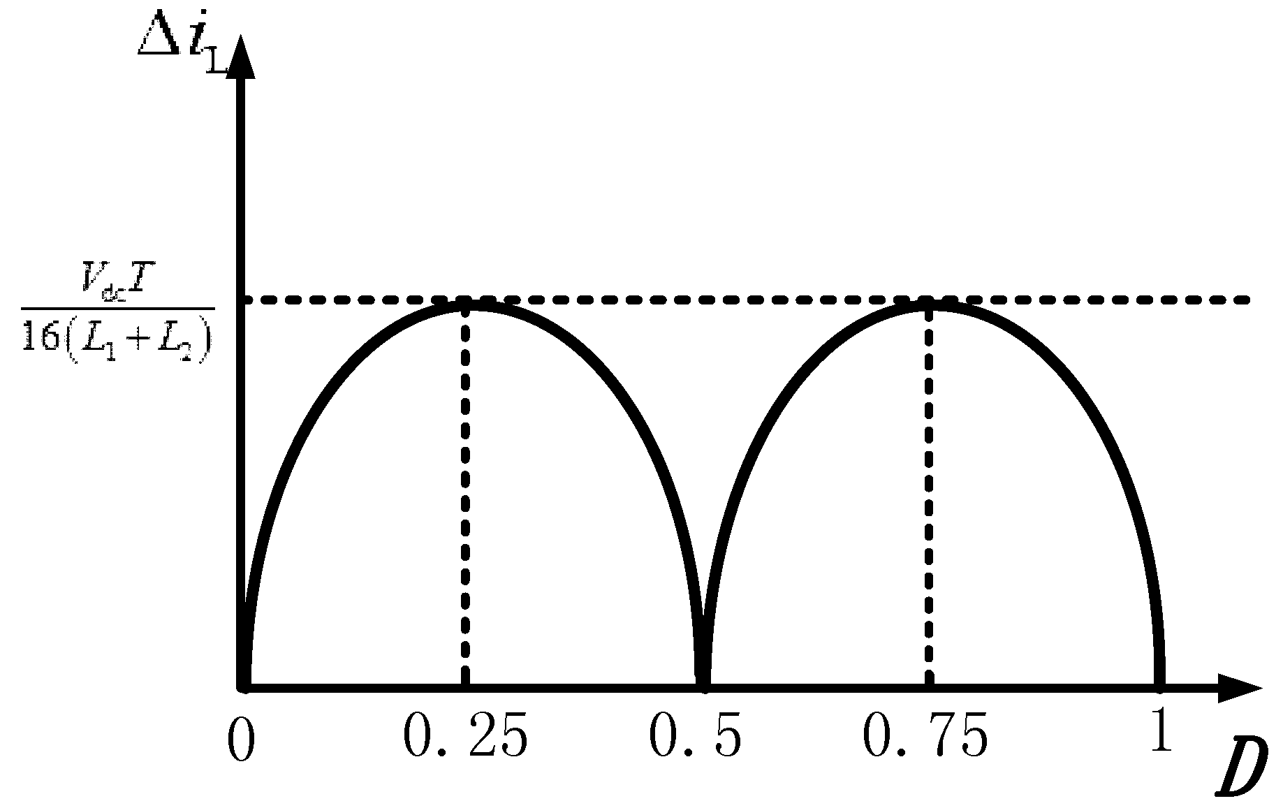
2.1.2. The Inductor Current Ripple Analysis
The converter output inductor current ripple ΔiL is derived for D > 0.5 and D < 0.5, respectively, through the operating waveforms, as shown in Figure 4 [34,35].
where T is the switching period, and D is the duty cycle.
Thus, the maximum output inductor current ripple ΔiLmax can be expressed as follows:
Figure 8 shows the graph for the relation between the duty cycle D and the output inductor current ripple ΔiL. As can be seen, the output inductor current ripple can reach the peak value ΔiLmax for D = 0.75 and D = 0.25, while the output inductor current ripple ΔiL is nearly zero for D = 0.5.
2.2. Back-End HFI LLC Resonant Converter
The structure of the back-end LLC resonant converter is demonstrated in Figure 9. The structure consists of the full-bridge inverter, a resonant tank, and a rectifier, which can achieve the high-frequency isolation (HFI) between the common DC bus and the EVs. The full-bridge inverter contains two parallel legs with four power switches S1–S4 including their anti-parallel diodes D1–D4 and parallel capacitors C1–C4. Meanwhile, the resonant tank is composed of the resonant capacitor Cr, the series resonant inductor Lr, and the high-frequency isolation (HFI) transformer, while the rectifier is composed of four diodes DR1–DR4. The resonant inductor Lr can be replaced by the leakage inductor of the transformer. The resonant capacitor Cr can also filter the DC component and prevent DC magnetic bias. The LLC resonant converters have advance characteristics of zero-voltage switching (ZVS) of inverter side and zero-current switching (ZCS) of the rectifier side. In particular, it can achieve better performance under quasi-resonant frequency mode and greatly reduce switching losses and improving system efficiency. The features of the back-end LLC resonant converter stated above have great advantages for power electronics transformer (PET) applications under high-voltage and high-power conditions.
2.2.1. Operating Principle
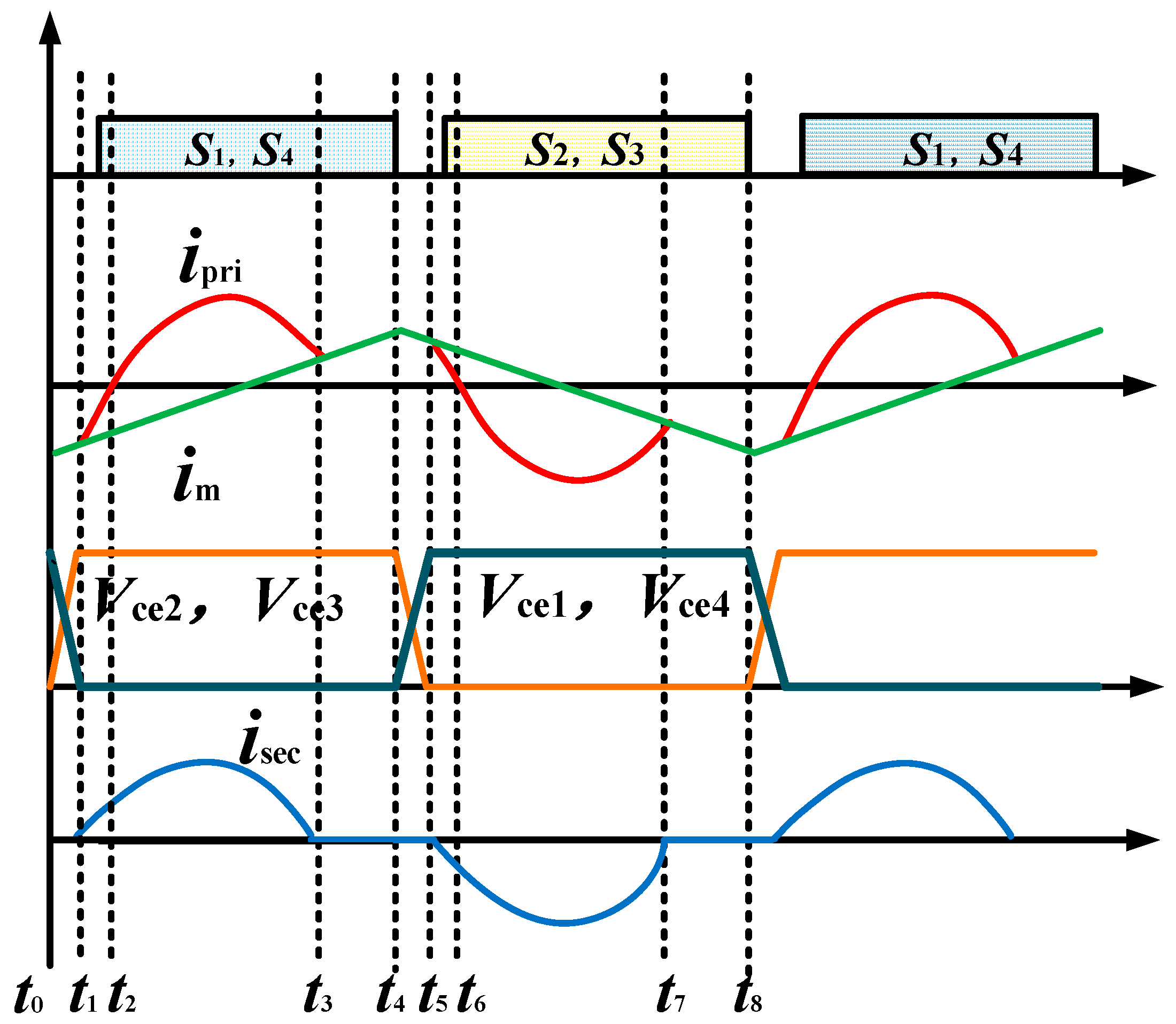
The operating principle and the key waveforms of the proposed back-end LLC resonant is shown in Figure 10, including the gate signals of active switches (S1–S4), the series resonant inductor current ipri, the magnetizing inductor current im, and the output current isec on the secondary side.
As for the resonant circuit, there are eight operation modes dependent on the direction of the primary current ipri and the inverter working conditions.
(1) Mode 1 (t0–t1)
This mode begins when S2 and S3 are turned off at t0, when the resonant inductor Lr current ipri flows in the negative direction. Meanwhile, the C1 and C4 discharge until Vce1 and Vce4 reach zero and the primary current ipri decreases. In this period, the magnetizing inductor current im is equivalent to ipri; thus, there is no induced current on the secondary side. The stored energy acquired by the output capacity CO is transferred to the load.
(2) Mode 2 (t1–t2)
In this mode, the ipri is still negative and will flow via the anti-parallel diodes of D1 and D4. The ZVS condition is achieved for S1 and S4. The magnetizing inductor current im increases linearly when isec begins to increase.
(3) Mode 3 (t2–t3)
This mode begins when the resonant inductor current ipri becomes positive. Now, the magnetizing inductor current im linearly increases with the resonant Lr while the resonant capacitor Cr works in a series-resonant condition. This mode ends when im and ipri are equal at t3. At the same time, the output current isec decays to zero. Both rectifier diodes DR1 and DR4 are turned off and ZCS is achieved.
(4) Mode 4 (t3–t4)
This mode begins when the resonant inductor current ipri is equal to the magnetizing inductor current im at t3, and both of them increase linearly while the isec is equal to zero. In this mode, the output is separated from the high-frequency transformer and the stored energy acquired by the output capacity CO is transferred to the load. This mode ends when S1 and S4 are turned off at t4.
For the next half cycle, the operation is opposite to the analysis above.
2.2.2. Voltage Gain Characteristics of the LLC Resonant Converter
As can be seen from Figure 11, the equivalent circuit diagram works under quasi-resonant frequency, in which Req is equivalent to the AC load of DC load R. The output DC load R is replaced by the equivalent AC load Req expressed as follows [36]:
where n is the transformer turn ratio.
To simplify the analysis, the input voltage can be equivalent to a square-wave voltage source Usquare, which needs to be Fourier-transformed:
Sinusoidal steady-state analysis is required for the equivalent electrical circuit. The output voltage under the frequency condition can be obtained by
Then, the instantaneous value of the output voltage is given by
The RMS of output voltage Uout yields
Hence, the LLC resonant converter voltage gain G is
where Um is the RMS of the square-wave voltage source.
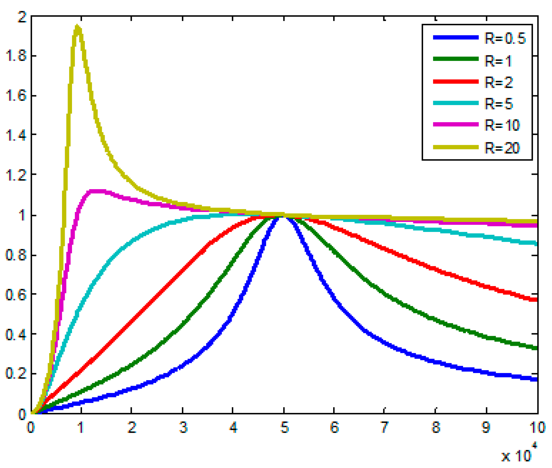
The value of Lr is the intrinsic parameter of the transformer, and the values of Lm and Cr are calculated by Equation (11). An LLC resonant converter with a 44 kHz resonant frequency has been designed, and the key parameters are Lr = 9.7 μH, Lm = 230 μH, and Cr = 1.32 μH. The experimental voltage gain characteristics of the LLC resonant converter under different load scenarios are shown in Figure 12 through the frequency response analyzer (VENABLE Model 3120). As can be observed in Figure 12, the LLC resonant converter shows the voltage gain characteristics, which are almost independent of the load when the switching frequency fs is around the resonant frequency fr called a quasi-resonant frequency. This is a distinct advantage of LLC resonant converter compared to the other DC-DC converters.
3. Features and Characteristics
3.1. Three-Level Buck Converter Working at Higher DC Modulation Index
The three-level buck converter is placed in front of the LLC resonant converter, which can help to obtain the desired output voltage with the higher modulation index D1 expressed in Equation (9) comparison to the other DC-DC converters:
The DC modulation index D2 of the traditional DC converter given by
where Vo is the output voltage, Vdc is the input voltage, and n is the transformer turn ratio. A step-down transformer (n > 1) has been used; hence, D1 > D2.
Taking the input voltage Vdc = 760 V and the output voltage Vo range from 200 to 500 V of the HFI DC–DC converter as an example. If n = 760/500, after the aforementioned calculation, the range of DC modulation index D1 is from 0.4 to 1, while the range of the DC modulation index D2 is from 0.26 to 0.65. Thus, the front-end three-level buck converter working at higher DC modulation index increases the voltage utilization ratio and improves efficiency.
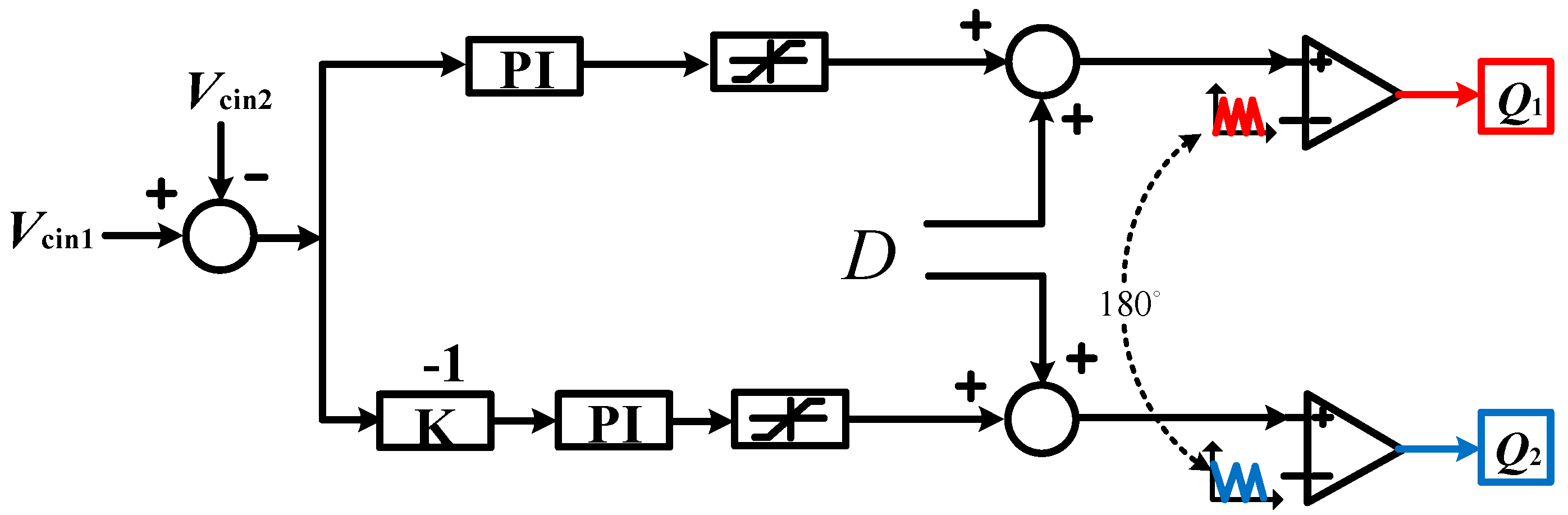
3.2. The Proposed DC Charging Port Having Different Power Balancing Capability for a Bipolar DC Bus
The split DC-link capacitors (Cin1, Cin2) connected on three-level buck converter are used as the interface between the bipolar DC buses. If there is a power imbalance in the bipolar DC bus, changing the DC modulation index of the upper and lower legs can balance the power between the DC buses. Figure 13 shows a diagram of power balance management. If the power on the positive DC side is higher than the negative DC side, it is necessary to increase the DC modulation index of the upper leg and reduce the DC modulation index of the lower leg. Therefore, the fast charger discharges more power from the positive to balance the bipolar DC bus. Alternatively, if the power on the positive DC side is less than the power on the negative DC side, it can balance the bipolar DC bus by adjusting the modulation index of the upper and lower legs.
3.3. LLC Resonant Converter Having ZVS Conditions with Different Magnetizing Current at Different Output Voltages
There is a condition for achieving ZVS:
The energy stored in the magnetizing inductor is larger than the energy stored in the switch parallel capacitance. According to [37], a generalized expression for magnetizing inductance is derived as
where td is the dead-time interval, N is the ratio of transformer, and is the parasitic capacitance.
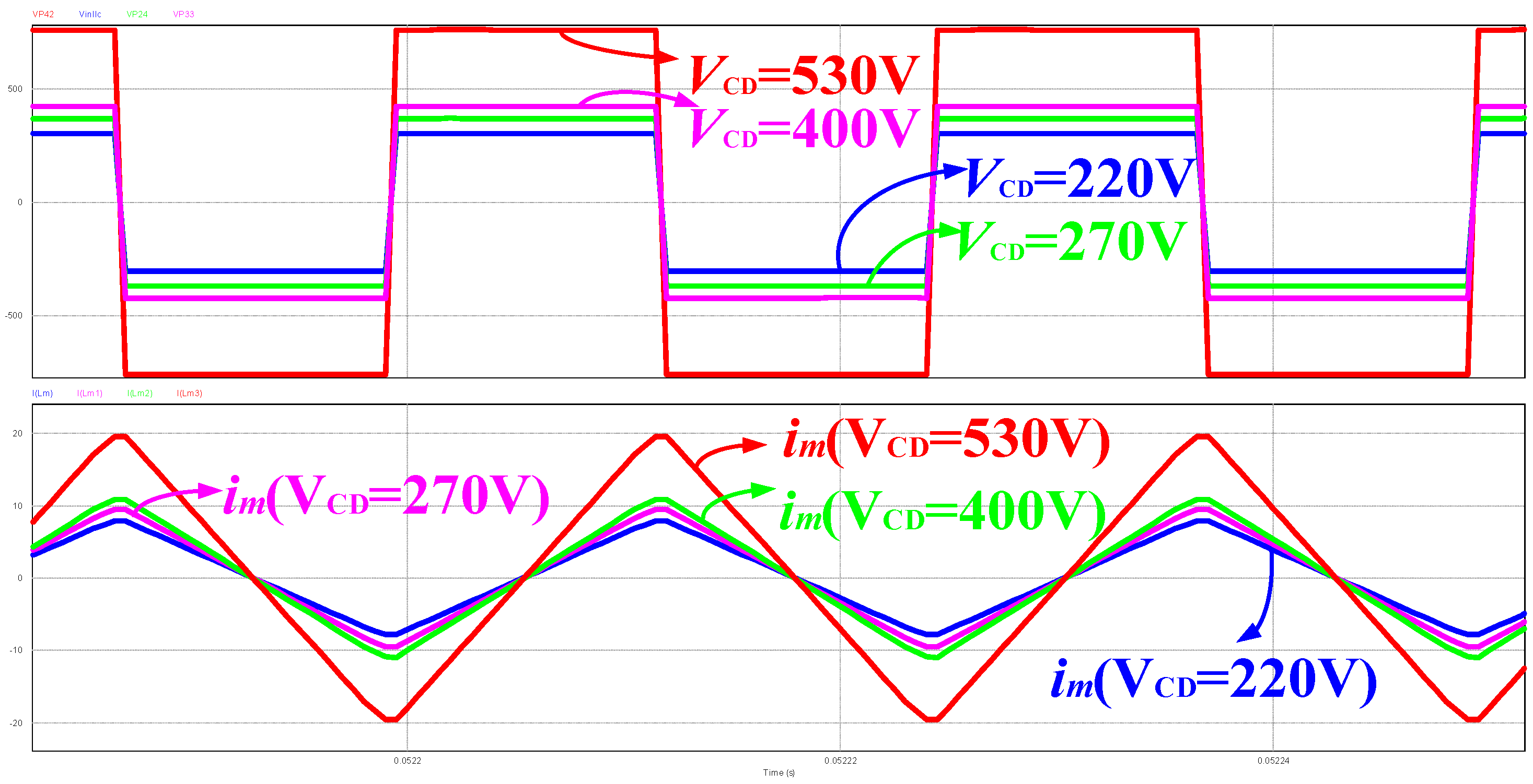
The structure of the proposed HFI charging port is shown in Figure 2. When the DC modulation index of front-end three-level buck converter was charged, the middle voltage Vm will also be changed, causing the magnetizing inductor current im to change. The simulation waveforms of magnetizing inductor im under different inverter output voltages (VCD) are shown in Figure 14. It can be clearly seen that im is changing with VCD, but the ZVS can be achieved by the magnetizing inductor Lm by drawing energy from the parallel capacitors C1–C4 until the energy stored in the parallel capacitance discharged thoroughly. This is because the voltage of parallel capacitor Vcex decreases to zero during the dead time, as the converter has the self-adaption ZVS condition.
3.4. LLC Resonant Converter Containing Constant Current at Different Output Voltages with the Same Charging Current Command
As the proposed back-end LLC resonant converter directly transfers power to the EV’s batteries, the output current remains constant whenever the output voltage changes in constant-current charging mode. The battery terminal voltage increases when the output current remains constant, while the input voltage Vm of LLC resonant converter increases along with the output voltage Vo, causing the magnetizing inductor current im to also increase. In order to maintain the output current io constant following the output voltage increasing, the resonant current ipri increases a little along with the magnetizing inductor current im. Therefore, the resonant current waveform is not affected by the output voltage Vo. On the contrary, if the LLC resonant converter is placed at the front end and is connected directly to the DC bus, the LLC input voltage Vin is clamped at the DC bus voltage Vdc. Thus, it keeps constant and the waveform of magnetizing inductor current is also constant. In this condition, the input current inevitably changes with the output voltage fluctuates in constant-current charging mode. Thus, the whole resonant process could not be optimized in different power conditions.
4. Design Conditions
4.1. Front-End Three-Level Buck Converter Inductor Filter Design
The maximum value of the filter inductor current ripple ΔiLmax can typically be 10–30% of the peak current:
Thus, the total filter inductor Lf can be derived as
The ΔiL reaches the maximum value for the duty cycle D = 0.25 and D = 0.75. A 20 kW prototype with a 760 V input DC voltage and a 200–500 V output DC voltage with a working frequency of fs = 20 kHz was built and tested. Based on the calculation above ΔILmax = 6 A, the filter inductor L1 = L2 = 200 μH can be derived. The next step is to select a suitable magnetic core and calculate the desirable turns N.
The front-end three-level buck converter can increase the equivalent switching twice using the PWM phase-shift control, so the frequency of inductor current ripple is 40 kHz. The formula of the Kool Mu window area Wa is derived as follows [38]:
where the utilization rate of the window Ku is 0.5, and the maximum magnetic flux density Bm is 0.45 T. The current density J is 400 A/cm2. Aε is the cross area of the wire.
Hence, according to Wa1Ae1 > 341 cm4, Wa1Ae1 = 350 cm4 is better for designing a necessary inductor in the Power Electronics Laboratory based on actual engineering problems. A magnetic core K8020E060 was selected, of which the window area Wa2 is 11.1 cm2, and the cross-sectional area Ae2 is 3.89 cm2. The number of magnetic core S can be shown to be
Based on Equation (15), the number S is 8. The inductor L can be denoted as
where AL is 190 nH; thus, the number of turns N = 17.
The experimental filter inductor prototype in accordance with the theoretical analysis mentioned above is presented in Figure 15.
4.2. Back-End LLC Converter ZVS Condition
For the back-end LLC resonant converter switches (S1–S4), the ZVS condition can satisfy from zero to full-load conditions because the magnetizing current im shown in Equation (17) is independent of the loads:
The input voltage Vin of the LLC resonant converter is clamped to the front-end buck converter regulated by the DC modulation index. The energy stored in the magnetizing inductor is sufficient for achieving ZVS for switches (S1–S4) within the voltage range. In this condition, another key point is regulating the dead time to satisfy the condition under which the energy stored in parallel capacitance can decay thoroughly.
4.3. High Frequency LLC Transformer Design
The high-frequency electrical isolation can be realized by the high-frequency transformer, which is the main component of the back-end LLC resonant converter with the bus converter function. The turn ratio n and the number of turns N are the key parameters for designing a high-frequency transformer. A 20 kW prototype with a 760 V input and a 200–500 V output DC voltages with a working frequency fs = 40 kHz was designed, so the turn ratio n (760/500) was adopted. The peak value of input voltage E1 can be calculated as follows:
where N1 is number of turns on the primary side, Acore is the cross-sectional area of the main magnetic circuit of the magnetic core, Bm is the maximum flux density, and f is the working frequency.
Thus, the number of turns on the secondary side N2 can be obtained:
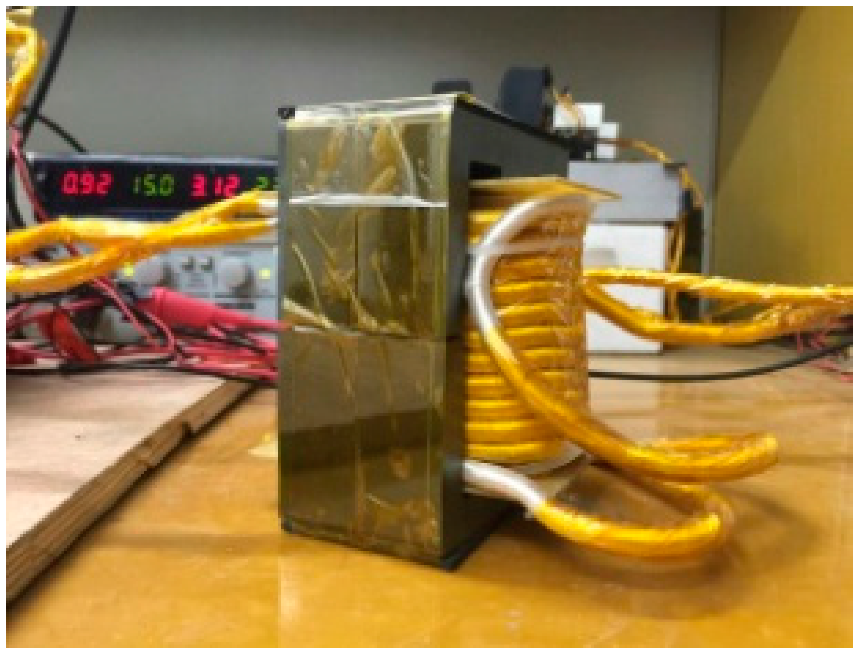
The experimental high-frequency LLC transformer is presented in Figure 16.
5. Experimental Results
The 20 kW prototype with an input voltage of 760 V and an 200–500 V output voltage, which integrates with the front-end three-level buck converter working at a frequency of 20 kHz and the back-end LLC resonant converter working at a frequency 40 kHz, was designed and tested. The experimental results are presented here to verify the validity and performance of the proposed fast-charging DC port system structure.
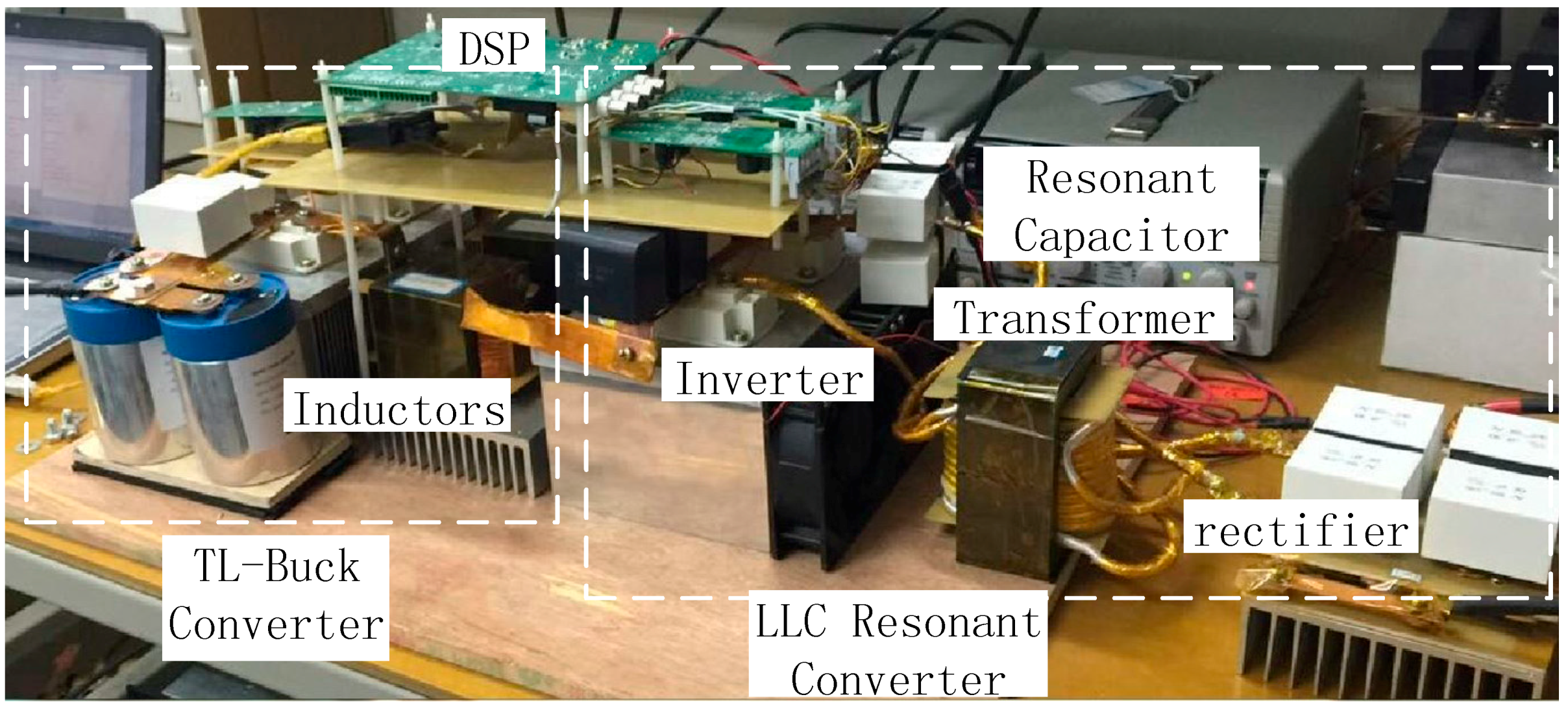
The photograph of the hardware prototype is shown in Figure 17, and the specifications of the prototype are shown in Table 2.
In the power electronics laboratory, the ITEM number of the resonant capacitor is C4BSYBX3330Z_F_, the manufacturer is KEMET, Un = 3000 V, and the value is 0.33 . The ITEM number of the rectifier diode is DSEI2X101-12A, and the manufacturer is IXYS. The ITEM number of the IGBT is SKM200GB125D, and the manufacturer is SEMIKRON INTERNATIONAL. The ITEM number of the voltage capacitance is SHK-700-540-FS, and the manufacturer is EACO. The ITEM number of the transformer core is K8020E060.
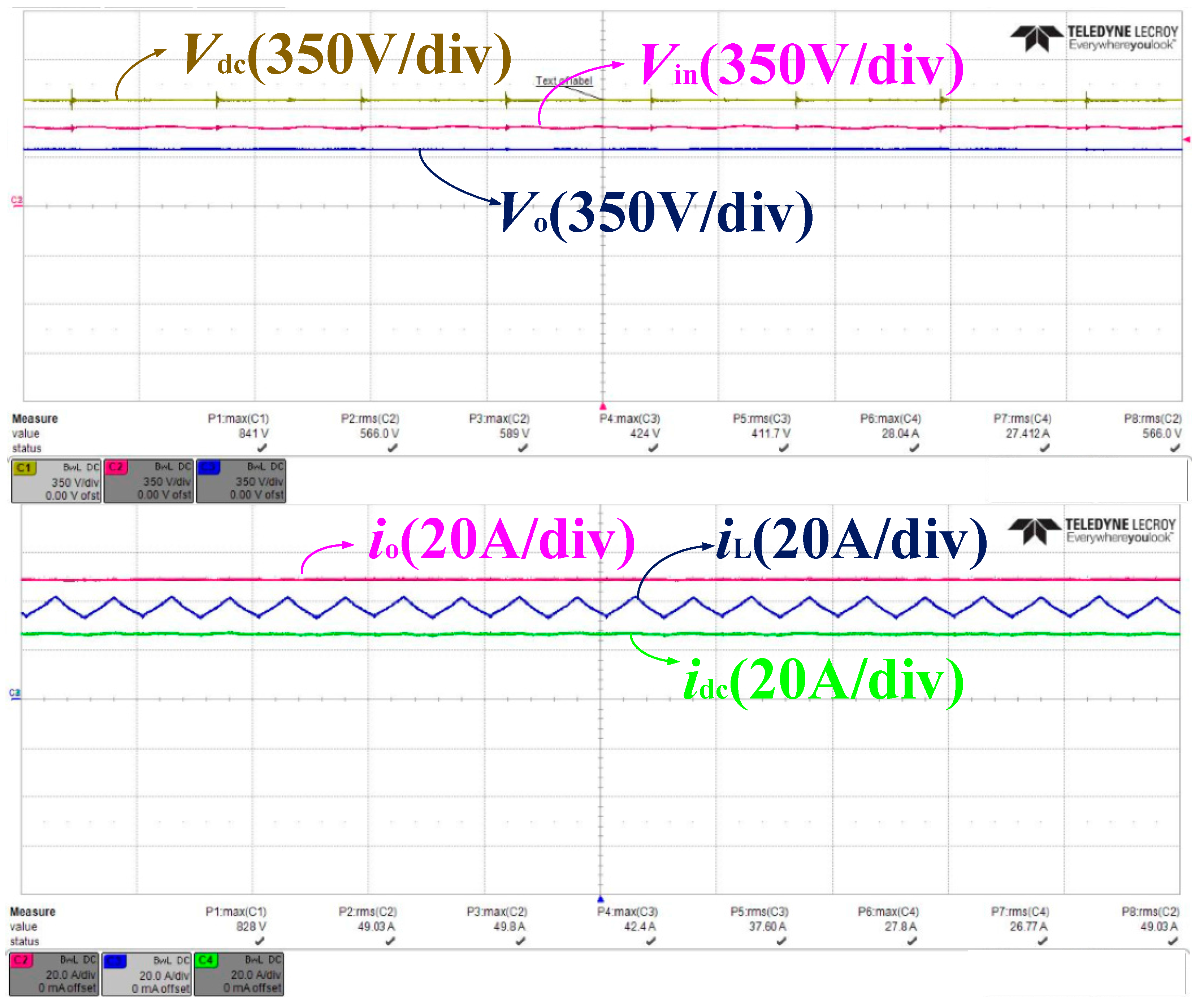
Figure 18 shows the waveforms of the proposed HFI charging DC port with D = 0.75; the total input voltage Vdc = 760 V, the LLC resonant converter input voltage Vin = 570 V, and the output voltage Vo = 400 V; the total input current idc = 26 A, the inductor current iL = 35 A, and the output current io = 50 A with the resistive DC load R0 = 8 Ω; the output power is about 20 kW. It can be seen that the system performs well while working in the steady-state operation and the experimental results are consistent with the theoretical analysis above.
5.1. In Steady-State Operation
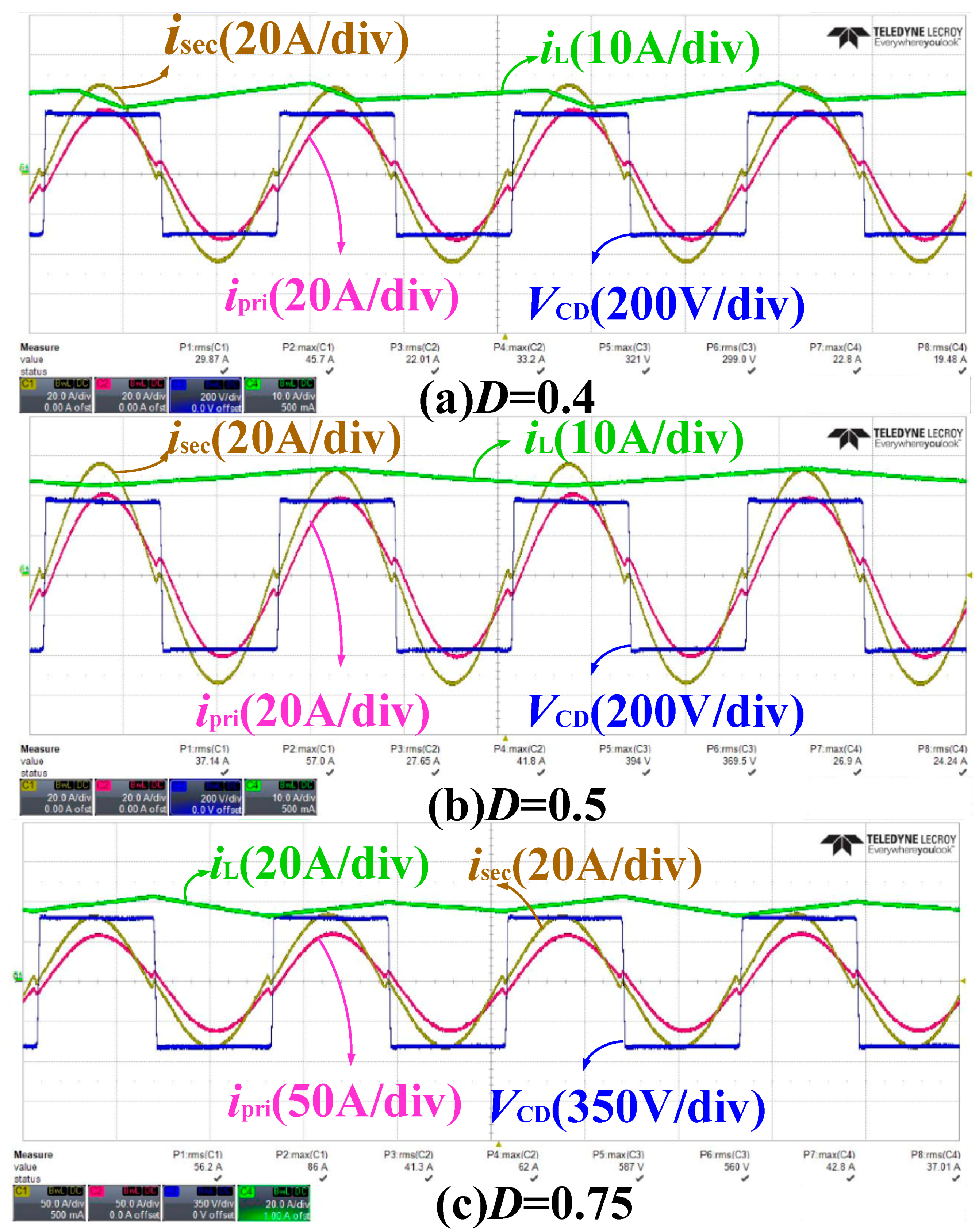
Figure 19 shows the experimental waveforms of the front-end three-level buck converter output voltage VAB and inductor current iL under different DC modulation indices (D = 0.4, D = 0.5, D = 0.75). The input voltage Vdc = 760 V and the load R0 = 8 Ω. As seen from Figure 20a, the VAB voltage is changed between 0 (Q1 and Q2 are off-state, D1 and D2 are on-state) and 380 V (Q1 and D2 are on-state or Q2 and D1 are on-state) for D = 0.4 and the output power is about 5.7 kW. The inductor current ripple ΔiL = 3.8 A is very close to the result of Equation (1). From Figure 20b, VAB is fixed at 380 V (Q1 and D2 are on-state or Q2 and D1 are on-state), and the inductor current ripple ΔiL almost reaches zero. This is because there is no voltage ripple on the filter inductors with D = 0.5, and the output power is nearly 9 kW. As can be seen from Figure 20c, VAB is changed between 380 V (Q1 and D2 are on-state or Q2 and D1 are on-state) and 760 V (both Q1 and Q2 are on-state) for D = 0.75 with about 20 kW of the output power. It can be found that the value of the output inductor current ripple reaches the maximum value ΔiLmax, which is about 6 A.
Figure 20 shows the experimental waveforms of the intermediate filter inductor current iL, the LLC primary side current ipri, the LLC secondary side current isec, and the LLC inverter-side output voltages (VCD) under different front-end modulation indices (with D = 0.4 having an output power of about 5.7 kW, D = 0.5 having an output power of about 9 kW, and D = 0.75 having an output power of about 20 kW). The input voltage, Vdc = 760 V, and the load, R0 = 8 Ω. It can be found that the primary side current ipri, secondary side current isec, and inverter-side output voltages VCD are changed due to different modulation indices. Additionally, the LLC resonant converter has good characteristics of zero-voltage switching (ZVS) with a different magnetizing inductor current im. The current waveforms on the primary side and secondary side present smooth curves that are consistent with the simulation results; thus, the viability and performance of the two power-stage system structure has been proved.
The ZVZCS characteristic curves of the back-end HFI LLC resonant converter under different modulation indices are shown in detail in Figure 21. The input voltage VCD = 760 V and the load, R0 = 8 Ω. Vce1 is the voltage of switch S1 and Vgs1 is the gate signal; ipri is the primary side current and isec is the secondary side current. It can be seen from Figure 21 that Vgs1 begins to turn on switch S1 after the Vce1 decreases to zero; thus, ZVS can be achieved from zero to full-load conditions. Additionally, ZCS can be achieved when isec reaches zero at the end of the resonant process under different output voltages conditions.
Figure 22 shows the experimental results of magnetizing inductor im current under different modulation indices D in detail under different power conditions. When the resonant process of Cr and Lr ends, the LLC primary-side ipri is the same as the magnetizing inductor current im. It can be seen that im is changing with the inverter-side output voltage VCD, the ZVS can be achieved adaptively and the circulating current is also decreased.
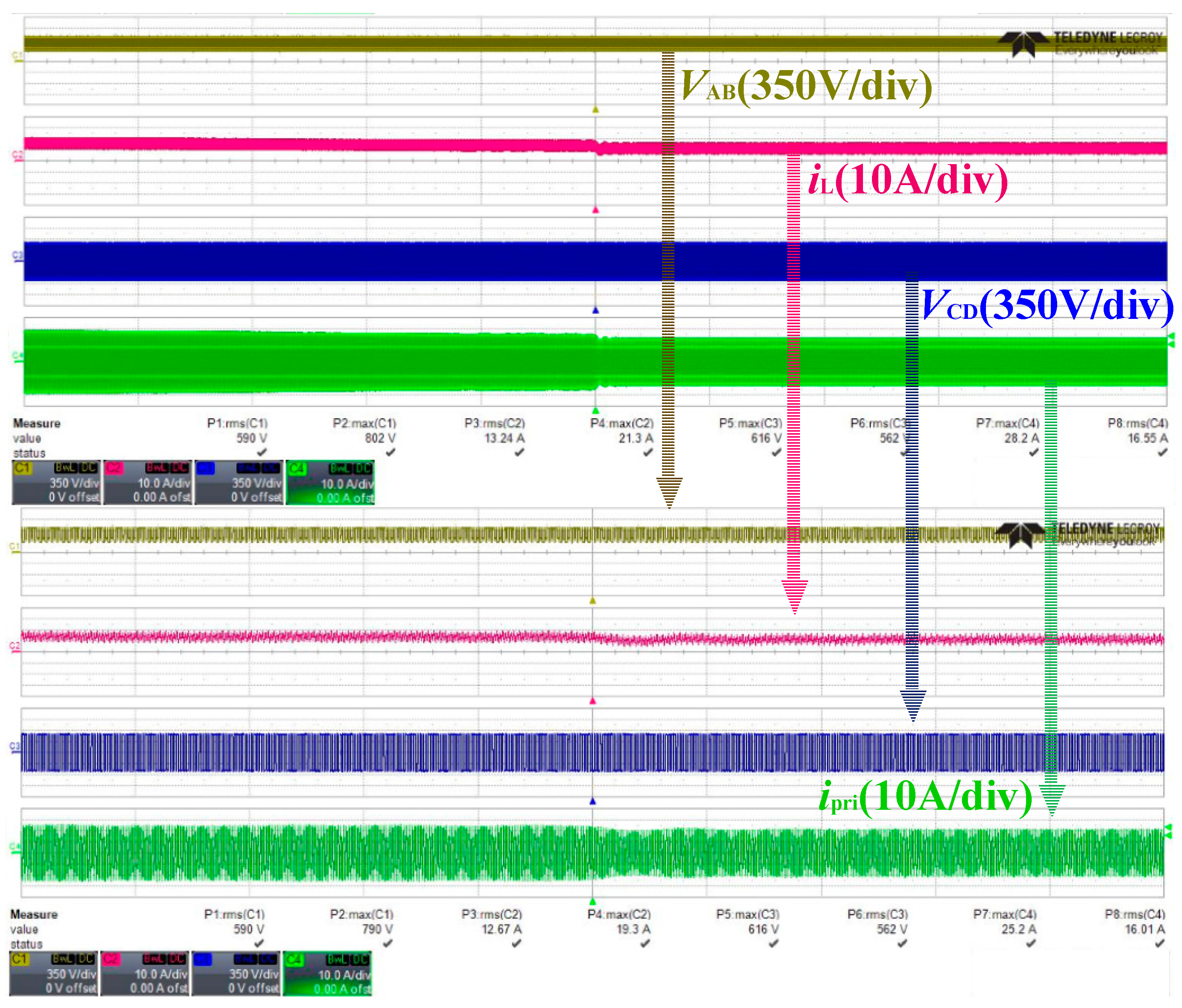
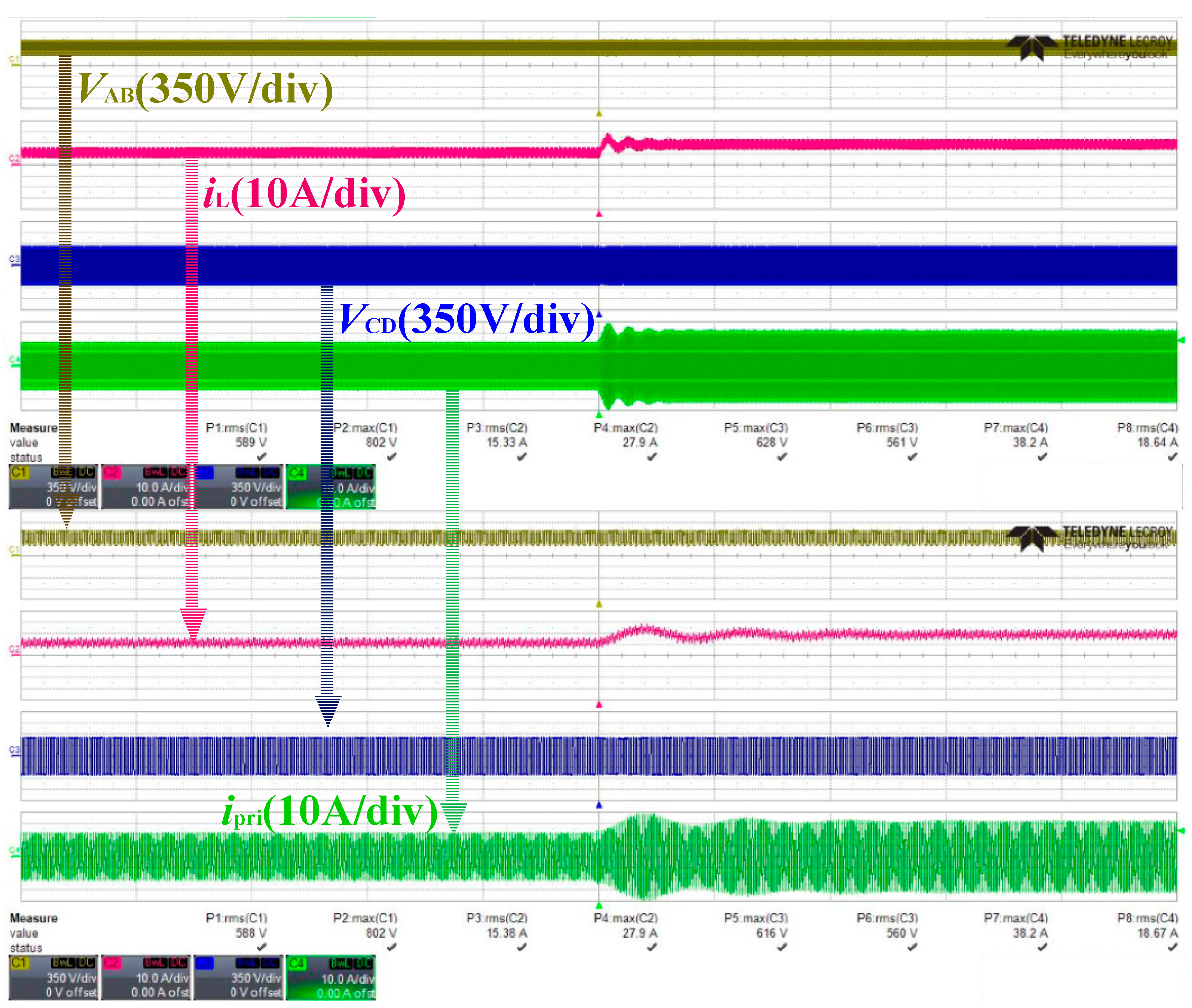
5.2. In the Load-Step Operation
In order to verify the viability and performance of the fast-charging DC port, dynamic-state experiments have been designed with changing loads. Figure 23 and Figure 24 show the transient experimental waveforms of the front-end three-level buck converter output voltage VAB, the inductor current iL, the LLC inverter-side output voltage VCD, and the primary side current ipri during a load step-up of the resistive load from 16 to 27 Ω and a load step-down of the resistive load from 27 to 16 Ω. As can be seen, the output voltages VAB and inverter output voltage VCD are independent of the resistive load, while the inductor current iL and the primary side current ipri reach a new stable state in a short time. Experimental results have shown that the proposed system structure can perform well under the conditions of a transient operation.
Finally, the experimental results above have shown the characteristic of the front-end three-level buck converter and the back-end LLC resonant converter in a steady-state operation and in a load-step operation. The validity and performance of the proposed HFI fast-charging DC port system structure has thus been proved.
6. Conclusions
A high-frequency-isolation (HFI) charging DC port can serve as the interface between unipolar/bipolar DC buses and electric-vehicles (EVs) based on a double power-stage system structure, which combines a front-end three-level converter with a back-end LLC resonant converter. Principles of the proposed charging port topology are studied in detail, while the features and characteristics are analyzed. Then, the design conditions of the three-level output filter and high-frequency isolation transformer are explored. Finally, a 20 kW prototype is designed and tested. The experimental results are presented to verify the validity and performance of the proposed HFI fast-charging DC port system structure.
Acknowledgments
This work is supported by the Science and Technology Foundation of Department of Education of Jilin Province (No. 201414002).
Author Contributions
Guowei Cai put forward the main idea and design of the entire venation of this paper. Duolun Liu performed the experiments and prepared the manuscript. Chuang Liu, Wei Li, and Jiajun Sun guided the experiments and wrote the paper.
Conflicts of Interest
The authors declare no conflict of interest.
References
- Tabari, M.; Yazdani, A. An energy management strategy for a DC distribution system for power system integration of Plug-In Electric Vehicles. IEEE Trans. Smart Grid 2016, 7, 659–668. [Google Scholar] [CrossRef]
- Korolko, N.; Sahinoglu, Z.; Nikovski, D. Modeling and forecasting self-similar power load due to EV fast chargers. IEEE Trans. Smart Grid 2016, 7, 1620–1629. [Google Scholar] [CrossRef]
- Liu, C.; Gu, B.; Lai, J.S.; Wang, M.; Ji, Y.; Cai, G.; Zhao, Z.; Chen, C.L.; Zheng, C.; Sun, P. High-efficiency hybrid full-bridge–half-bridge converter with shared ZVS lagging leg and dual outputs in series. IEEE Trans. Power Electron. 2013, 28, 849–861. [Google Scholar] [CrossRef]
- Goli, P.; Shireen, W. PV integrated smart charging of PHEVs based on DC link voltage sensing. IEEE Trans. Smart Grid 2014, 5, 1421–1428. [Google Scholar] [CrossRef]
- Dubey, A.; Santoso, S.; Cloud, M.P. Average-value model of electric vehicle chargers. IEEE Trans. Smart Grid 2013, 4, 1549–1557. [Google Scholar] [CrossRef]
- Hredzak, B.; Agelidis, V.G.; Jang, M. A model predictive control system for a hybrid battery-ultracapacitor power source. IEEE Trans. Power Electron. 2014, 29, 1469–1479. [Google Scholar] [CrossRef]
- Channegowda, J.; Pathipati, V.K.; Williamson, S.S. Comprehensive review and comparison of DC fast charging converter topologies: Improving electric vehicle plug-to-wheels efficiency. In Proceedings of the 2015 IEEE 24th International Symposium on Industrial Electronics (ISIE 2015), Buzios, Brazil, 3–5 June 2015; pp. 263–268. [Google Scholar]
- Musavi, F.; Edington, M.; Eberle, W.; Dunford, W.G. Evaluation and efficiency comparison of front end AC-DC plug-in hybrid charger topologies. IEEE Trans. Smart Grid 2012, 3, 413–421. [Google Scholar] [CrossRef]
- Machiels, N.; Leemput, N.; Geth, F.; Van Roy, J.; Büscher, J.; Driesen, J. Design criteria for electric vehicle fast charge infrastructure based on flemish mobility behavior. IEEE Trans. Smart Grid 2014, 5, 320–327. [Google Scholar] [CrossRef]
- Bai, S.; Lukic, S.M. Unified active filter and energy storage system for an MW electric vehicle charging station. IEEE Trans. Power Electron. 2013, 28, 5793–5803. [Google Scholar] [CrossRef]
- Corchero, C.; Cruz-Zambrano, M.; Heredia, F.J. Optimal energy management for a residential microgrid including a vehicle-to-grid system. IEEE Trans. Smart Grid 2014, 5, 2163–2172. [Google Scholar]
- Atia, R.; Yamada, N. Sizing and analysis of renewable energy and battery systems in residential microgrids. IEEE Trans. Smart Grid 2016, 73, 1204–1213. [Google Scholar] [CrossRef]
- Lakshminarayana, S.; Xu, Y.; Poor, H.V.; Quek, T.Q. Cooperation of storage operation in a power network with renewable generation. IEEE Trans. Smart Grid 2016, 7, 2108–2122. [Google Scholar] [CrossRef]
- Oliveira, T.R.; Silva, W.W.A.G.; Donoso-Garcia, P.F. Distributed secondary level control for energy storage management in dc microgrids. IEEE Trans. Smart Grid 2016, 1–11. [Google Scholar] [CrossRef]
- Falcones, S.; Ayyanar, R.; Mao, X. A DC–DC multiport-converter-based solid-state transformer integrating distributed generation and storage. IEEE Trans. Power Electron. 2013, 28, 2192–2203. [Google Scholar] [CrossRef]
- Shin, C.J.; Lee, J.Y. An electrolytic capacitor-less bi-directional EV on-board charger using harmonic modulation technique. IEEE Trans. Power Electron. 2014, 29, 5195–5203. [Google Scholar] [CrossRef]
- Rivera, S.; Wu, B.; Kouro, S.; Yaramasu, V.; Wang, J. Electric vehicle charging station using a neutral point clamped converter with bipolar DC bus. IEEE Trans. Ind. Electron. 2015, 62, 1999–2009. [Google Scholar] [CrossRef]
- Liu, C.; Sun, P.; Lai, J.S.; Ji, Y.; Wang, M.; Chen, C.L.; Cai, G. Cascade dual-boost/buck active-front-end converter for intelligent universal transformer. IEEE Trans. Ind. Electron. 2012, 59, 4671–4680. [Google Scholar]
- Tan, L.; Wu, B.; Rivera, S.; Yaramasu, V. Comprehensive DC power balance management in high-power three-level DC–DC converter for electric vehicle fast charging. IEEE Trans. Power Electron. 2016, 31, 89–100. [Google Scholar] [CrossRef]
- SAE Electric Vehicle and Plug-in Hybrid Electric Vehicle Conductive Charge Coupler; J1772; SAE International: Warrendale, PA, USA, 2010.
- Yilmaz, M.; Krein, P.T. Review of battery charger topologies, charging power levels, and infrastructure for plug-in electric and hybrid vehicles. IEEE Trans. Power Electron. 2013, 28, 2151–2169. [Google Scholar] [CrossRef]
- Vasiladiotis, M.; Rufer, A. A modular multiport power electronic transformer with integrated split battery energy storage for versatile ultrafast EV charging stations. IEEE Trans. Ind. Electron. 2015, 62, 3213–3222. [Google Scholar] [CrossRef]
- Dusmez, S.; Khaligh, A. A compact and integrated multifunctional power electronic interface for plug-in electric vehicles. IEEE Trans. Power Electron. 2013, 28, 5690–5701. [Google Scholar] [CrossRef]
- Lu, X.; Iyer, K.L.V.; Mukherjee, K.; Kar, N.C. A dual purpose triangular neural network based module for monitoring and protection in Bi-directional off-board level-3 charging of EV/PHEV. IEEE Trans. Smart Grid 2012, 3, 1670–1678. [Google Scholar] [CrossRef]
- Wang, Z.; Li, H. An integrated three-port bidirectional DC–DC converter for PV application on a DC distribution system. IEEE Trans. Power Electron. 2013, 28, 4612–4624. [Google Scholar] [CrossRef]
- Kim, S.Y.; Song, H.S.; Nam, K. Idling port isolation control of three-port bidirectional converter for EVs. IEEE Trans. Power Electron. 2012, 27, 2495–2506. [Google Scholar] [CrossRef]
- Kim, S.; Kang, F.S. Multifunctional onboard battery charger for plug-in electric vehicles. IEEE Trans. Ind. Electron. 2015, 62, 3460–3472. [Google Scholar]
- Subotic, I.; Bodo, N.; Levi, E.; Jones, M.; Levi, V. Isolated chargers for EVs incorporating six-phase machines. IEEE Trans. Ind. Electron. 2016, 63, 653–664. [Google Scholar] [CrossRef]
- Everts, J.; Krismer, F.; Van Den Keybus, J.; Driesen, J.; Kolar, J.W. Optimal ZVS modulation of single-phase single-stage bidirectional DAB AC–DC converters. IEEE Trans. Power Electron. 2014, 29, 3954–3970. [Google Scholar] [CrossRef]
- Gu, B.; Lai, J.S.; Kees, N.; Zheng, C. Hybrid-switching full-bridge DC–DC converter with minimal voltage stress of bridge rectifier, reduced circulating losses, and filter requirement for electric vehicle battery chargers. IEEE Trans. Power Electron. 2013, 28, 1132–1144. [Google Scholar] [CrossRef]
- Tan, X.; Ruan, X. Equivalence relations of resonant tanks: A new perspective for selection and design of resonant converters. IEEE Trans. Ind. Electron. 2016, 63, 2111–2123. [Google Scholar] [CrossRef]
- Kheraluwala, M.N.; Gascoigne, R.W.; Divan, D.M.; Baumann, E.D. Performance characterization of a high-power dual active bridge DC-to-DC converter. IEEE Trans. Ind. Appl. 1992, 28, 1294–1301. [Google Scholar] [CrossRef]
- Haihua, Z.; Khambadkone, A.M. Hybrid modulation for dual active bridge bi-directional converter with extended power range for ultra-capacitor application. In Proceedings of the IEEE Industry Applications Society Annual Meeting, Edmonton, AB, Canada, 5–9 October 2008; pp. 1–8. [Google Scholar]
- Pinheiro, J.R.; Barbi, I. The three-level ZVS PWM converter-a new concept in high voltage DC-to-DC conversion. In Proceedings of the 1992 International Conference on Industrial Electronics, Control, Instrumentation, and Automation, San Diego, CA, USA, 13 November 1992; pp. 173–178. [Google Scholar]
- Ruan, X.; Li, B.; Chen, Q. Three-level converters—A new approach for high voltage and high power DC-to-DC conversion. In Proceedings of the 2002 IEEE 33rd Annual IEEE Power Electronics Specialists Conference, Cairns, Queensland, Australia, 23–27 June 2002; Volume 2, pp. 663–668. [Google Scholar]
- Steigerwald, R.L. A comparison of half-bridge resonant converter topologies. IEEE Trans. Power Electron. 1988, 3, 174–182. [Google Scholar] [CrossRef]
- Kundu, U.; Yenduri, K.; Sensarma, P. Accurate ZVS Analysis for Magnetic Design and Efficiency Improvement of Full-Bridge LLC Resonant Converter. IEEE Trans. Power Electron. 2017, 32, 1703–1706. [Google Scholar] [CrossRef]
- Hurley, W.G.; Wolfle, W.H. Transformers and Inductors for Power Electronics: Theory, Design and Applications; China Machine Press: Beijing, China, 2014; pp. 46–47. [Google Scholar]
Figure 1.
System block diagram of a fast electric vehicle (EV) charging station based on the common DC bus.
Figure 1.
System block diagram of a fast electric vehicle (EV) charging station based on the common DC bus.
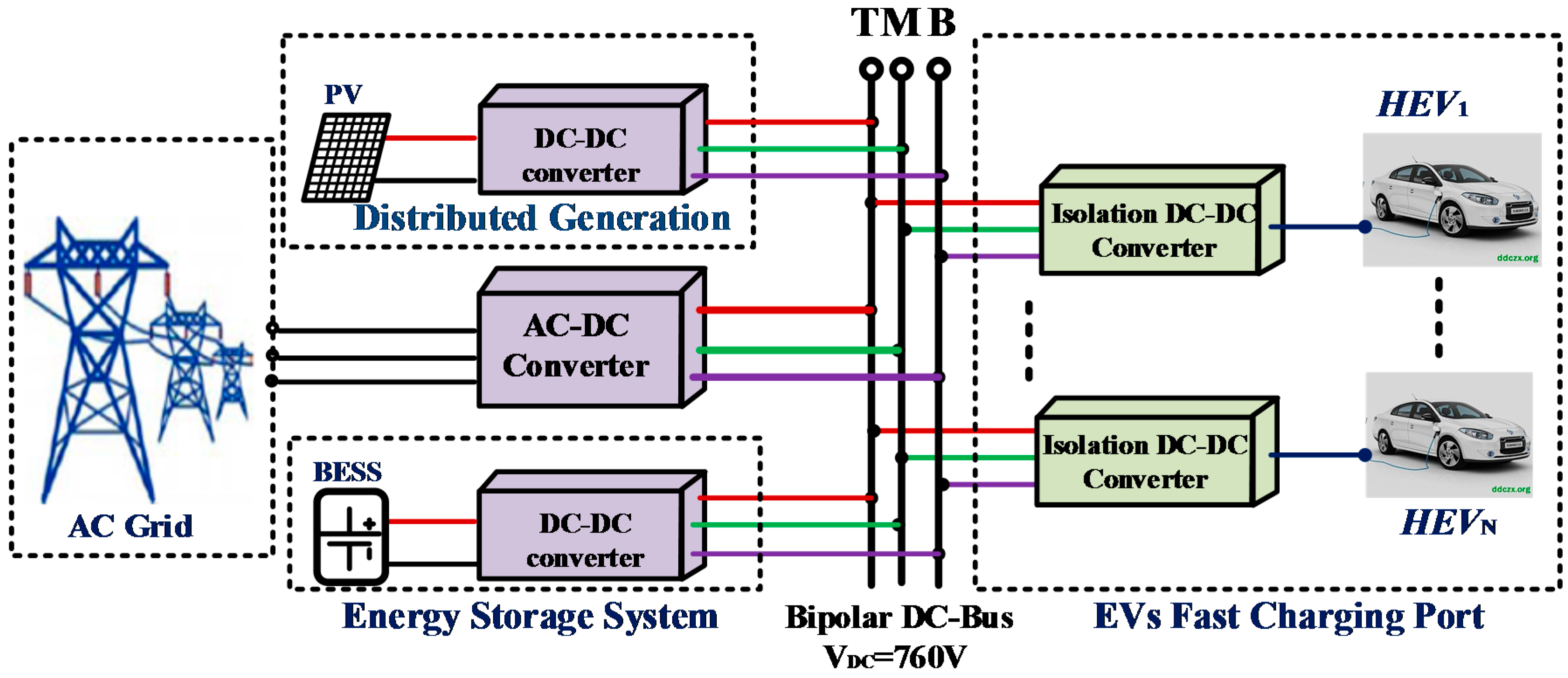
Figure 2.
The proposed high-frequency isolation (HFI) charging-port topology based on a front-end three-level converter and a back-end LLC resonant converter.
Figure 2.
The proposed high-frequency isolation (HFI) charging-port topology based on a front-end three-level converter and a back-end LLC resonant converter.

Figure 3.
Front-end three-level buck converter topology.

Figure 4.
Main theoretical waveforms of the front-end three-level buck converter. (a) D < 0.5; (b) D = 0.5; (c) D > 0.5.
Figure 4.
Main theoretical waveforms of the front-end three-level buck converter. (a) D < 0.5; (b) D = 0.5; (c) D > 0.5.

Figure 5.
Operating stages and equivalent circuits for D > 0.5.

Figure 6.
Operating stages and equivalent circuits for D = 0.5.
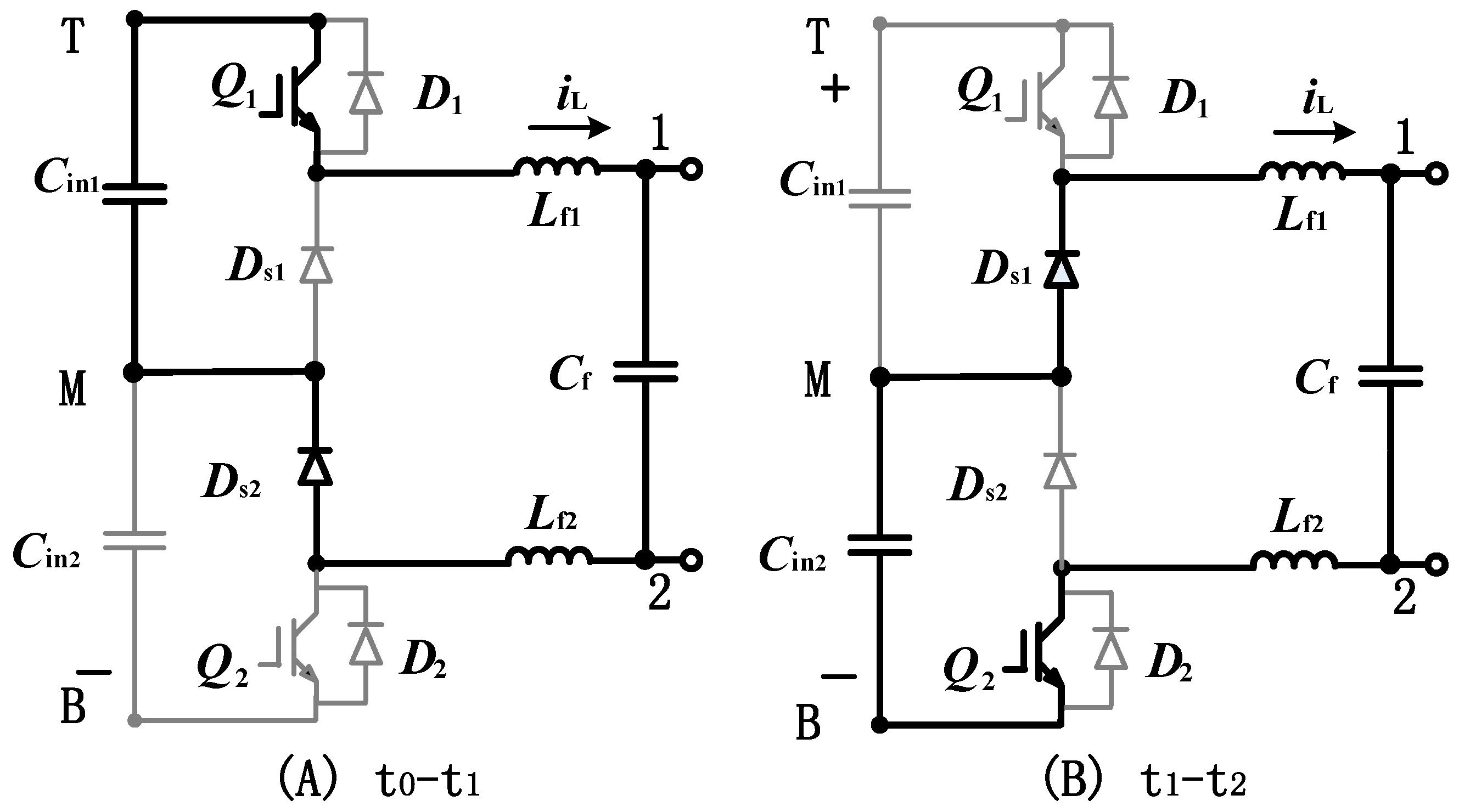
Figure 7.
Operating stages and equivalent circuits for D < 0.5.
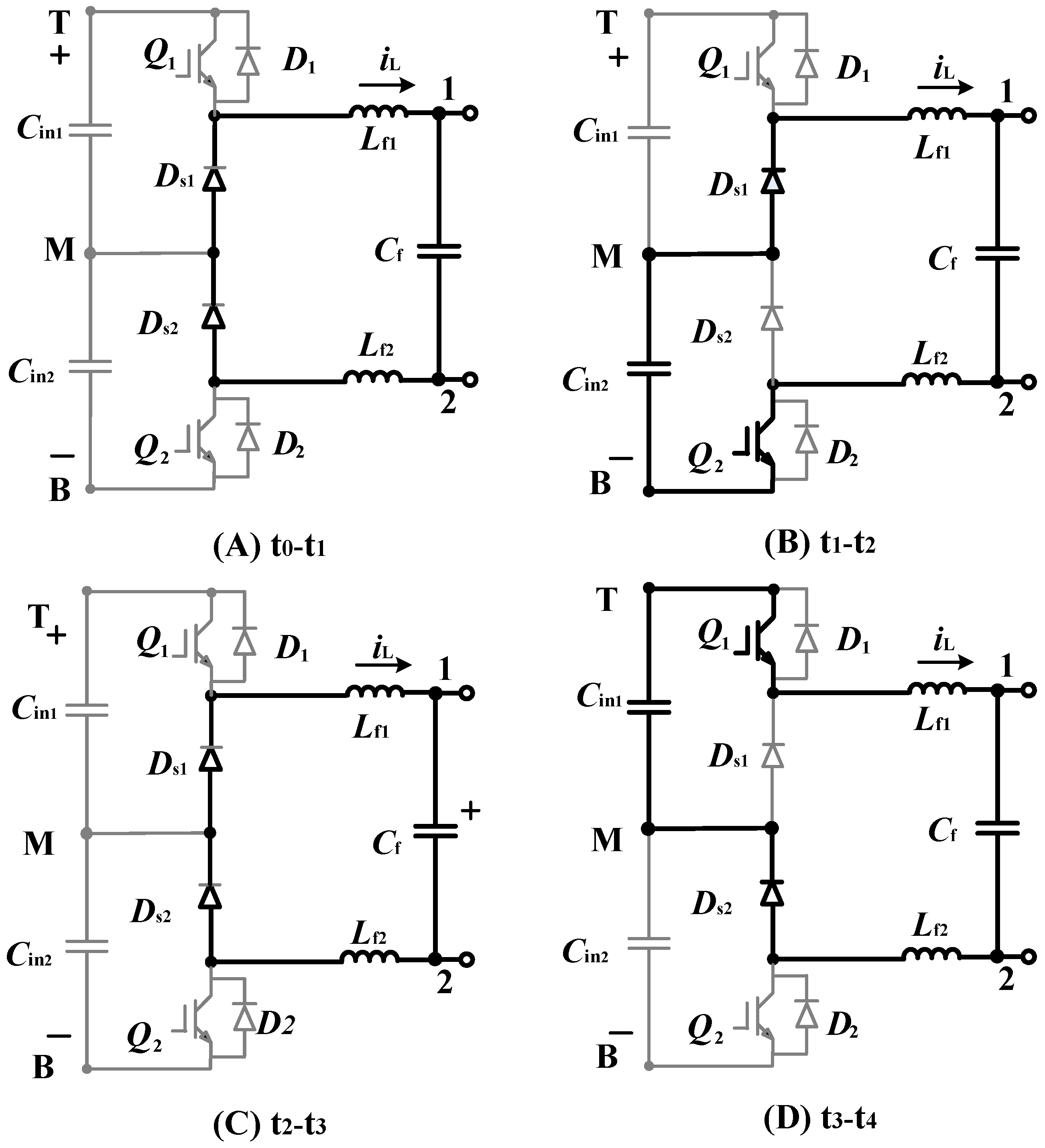
Figure 8.
The relation between the duty cycle D and the output inductor current ripple ΔiL.

Figure 9.
Back-end HFI LLC resonant converter.
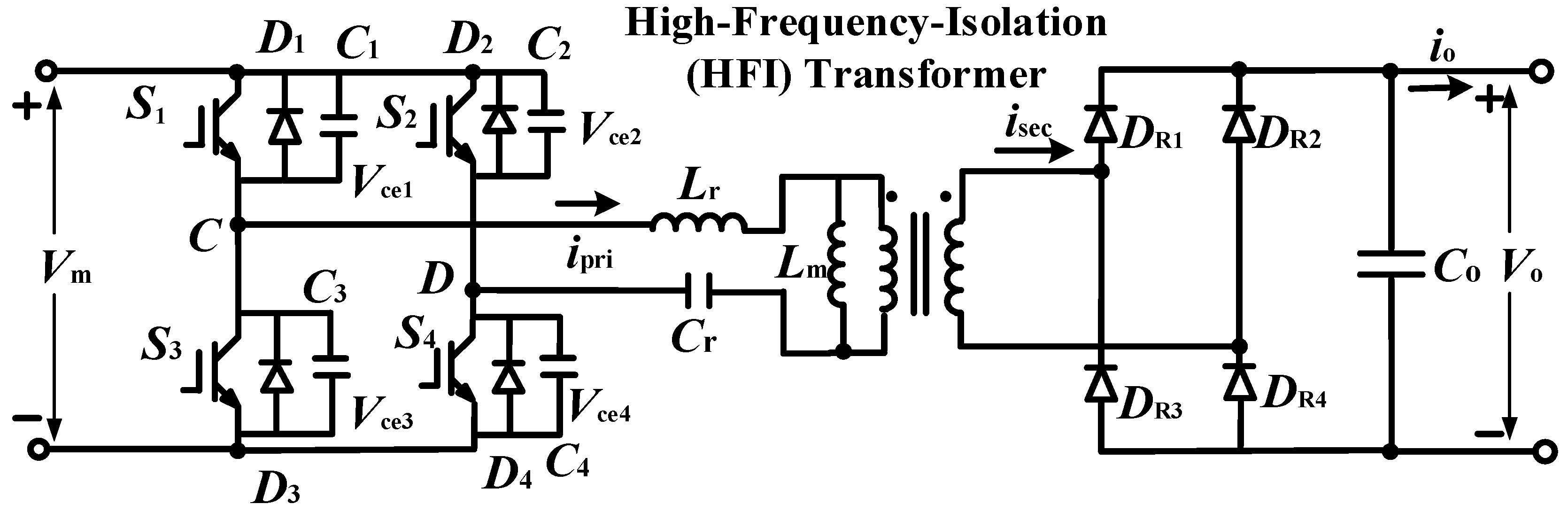
Figure 10.
Operating waveforms of the back-end HFI LLC resonant converter.

Figure 11.
Equivalent circuit for the back-end LLC resonant converter.

Figure 12.
Voltage gain characteristics of LLC resonant converters.

Figure 13.
Modulation block diagram of the front-end three-level buck converter.

Figure 14.
Simulation waveform of magnetizing inductor current under different VCD values.

Figure 15.
Front-end three-level buck converter inductor filter.

Figure 16.
High-frequency LLC transformer.

Figure 17.
The HFI fast-charging DC port system experimental setup.

Figure 18.
Experimental results of the converter in the steady-state operation.

Figure 19.
Experimental results of the front-end three-level buck converter (a) D = 0.4; (b) D = 0.5; (c) D = 0.75.
Figure 19.
Experimental results of the front-end three-level buck converter (a) D = 0.4; (b) D = 0.5; (c) D = 0.75.
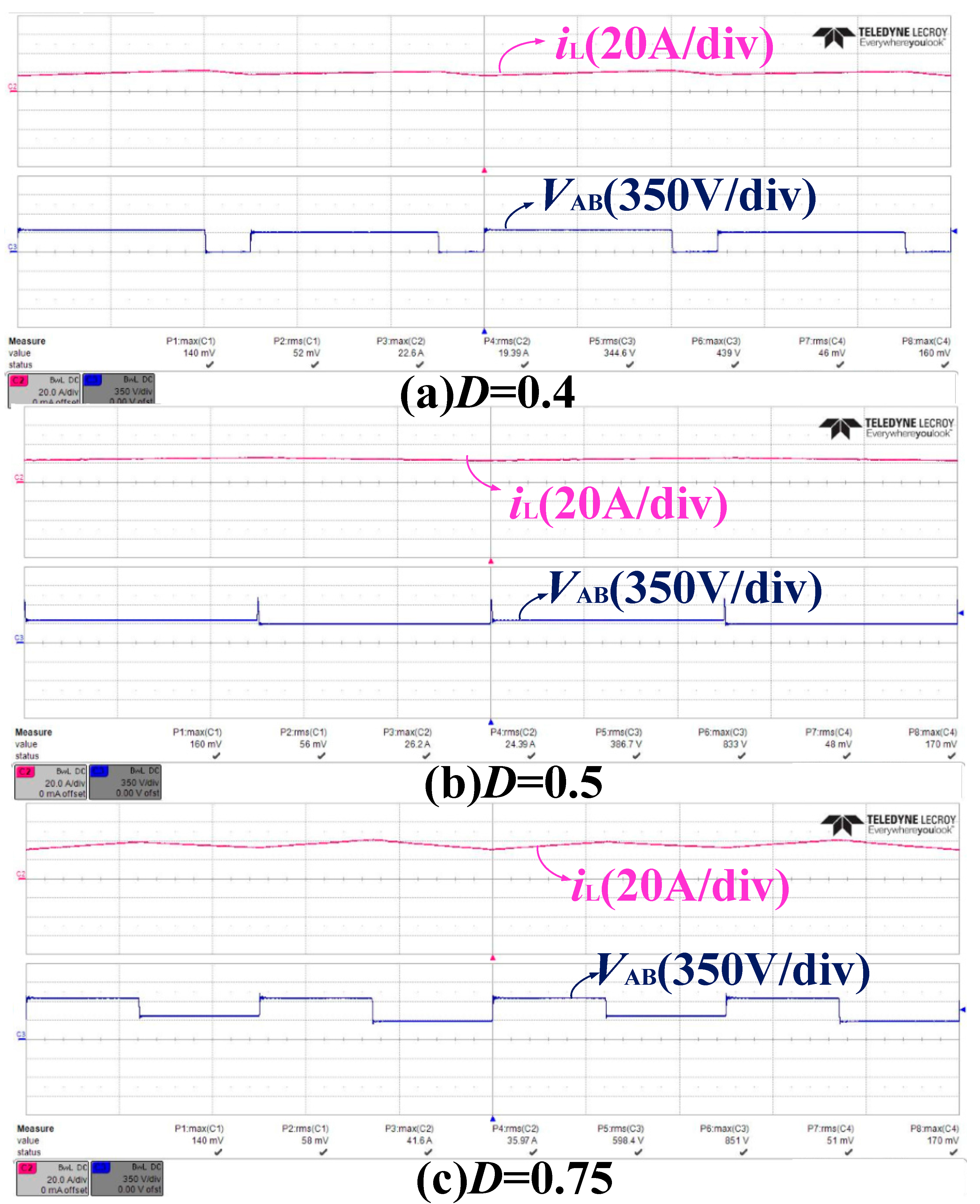
Figure 20.
Experimental results of the back-end HFI LLC resonant converter (a) D = 0.4; (b) D = 0.5; (c) D = 0.75.
Figure 20.
Experimental results of the back-end HFI LLC resonant converter (a) D = 0.4; (b) D = 0.5; (c) D = 0.75.

Figure 21.
Back-end HFI LLC resonant converter ZVZCS characteristic curves (a) D = 0.4; (b) D = 0.5; (c) D = 0.75.
Figure 21.
Back-end HFI LLC resonant converter ZVZCS characteristic curves (a) D = 0.4; (b) D = 0.5; (c) D = 0.75.
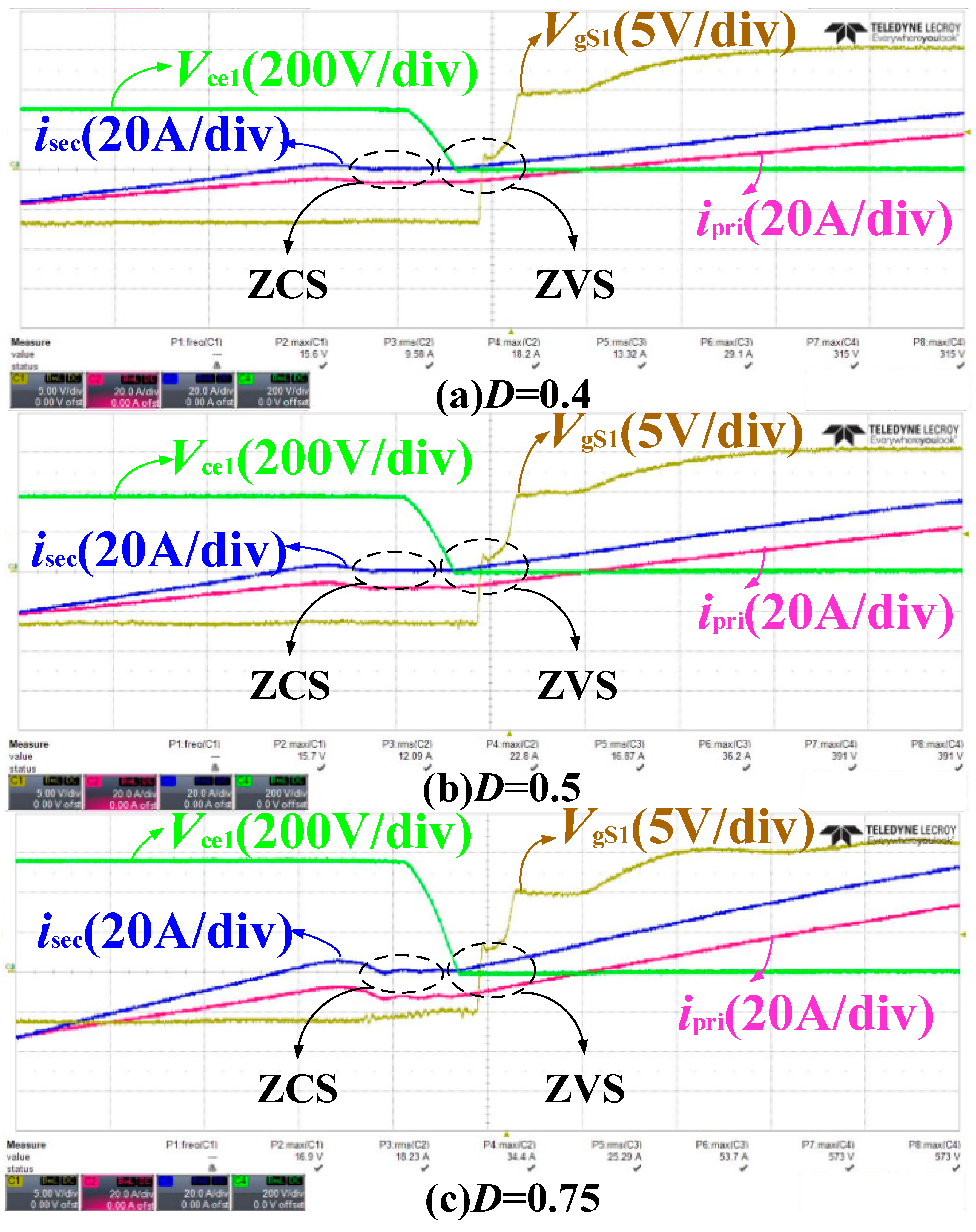
Figure 22.
Experimental waveforms of the magnetizing inductor current under different modulation indices D.
Figure 22.
Experimental waveforms of the magnetizing inductor current under different modulation indices D.
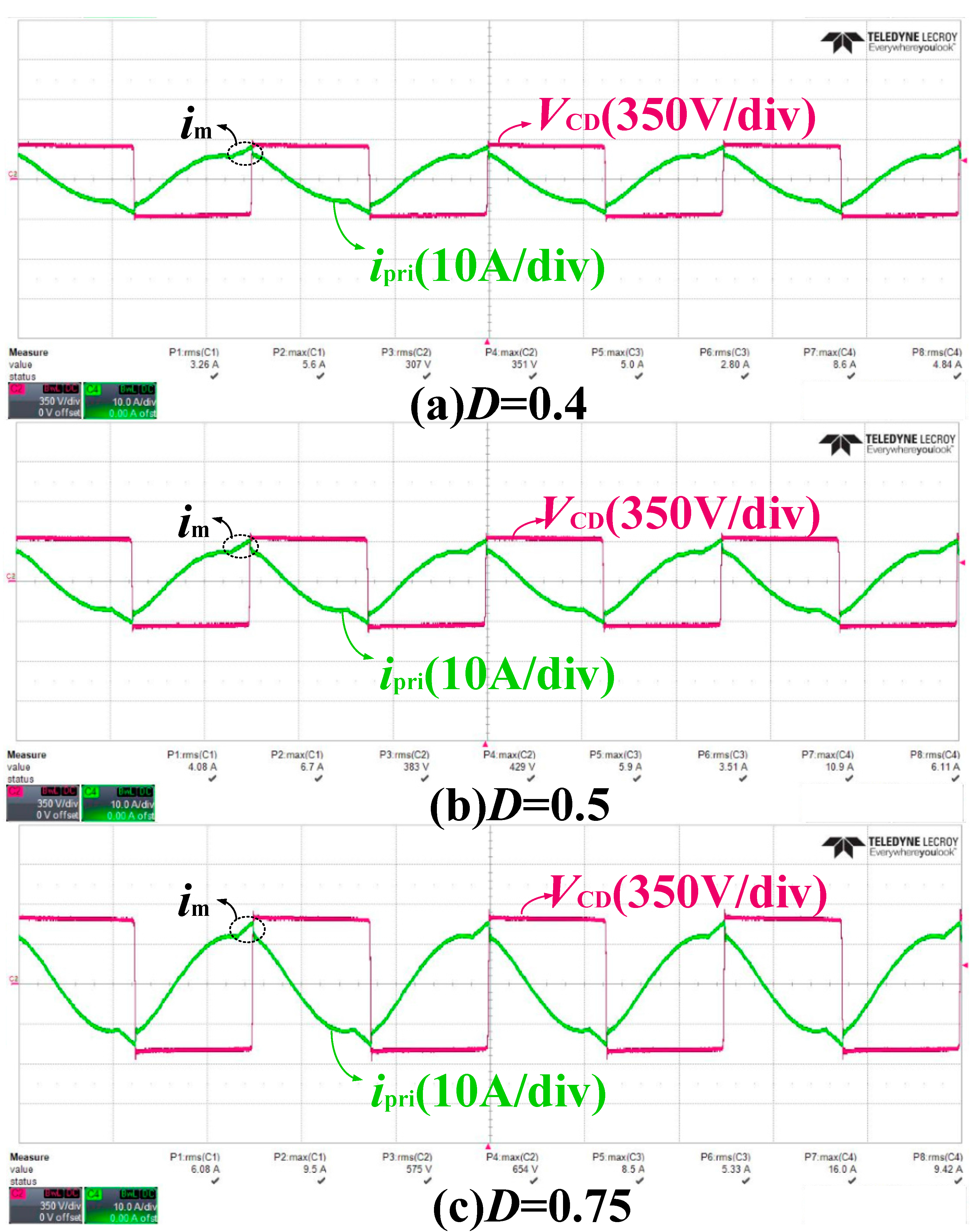
Figure 23.
Transient waveforms during a step-up of resistive load from R0 = 16 Ω to R0 = 27 Ω.

Figure 24.
Transient waveforms during a step-down of the resistive load from R0 = 27 Ω to R0 = 16 Ω.
Figure 24.
Transient waveforms during a step-down of the resistive load from R0 = 27 Ω to R0 = 16 Ω.


Table 1.
Converter specifications and requirements.
| Charger Location | Level 1 | Level 2 | Level 3 | |
|---|---|---|---|---|
| On-board chargers | Vac | 120 V | 240 V | - |
| Iac | 12 A | 80 A | - | |
| Plevel | 1.4 kW | <19.2 kW | >20 kW | |
| Off-board chargers | Vdc (V) | Vdc ≤ 450 | Vdc ≤ 450 | Vdc ≤ 600 |
| Idc (A) | Idc ≤ 80 | Idc ≤ 200 | Idc ≤ 400 | |
| Plevel (kW) | Plevel ≤ 36 | Plevel ≤ 90 | Plevel ≤ 240 | |
Table 2.
Circuit parameters of the HFI fast-charging DC port system.
| Description | Parameters |
|---|---|
| Input voltage Vdc | 760 V (DC) |
| Output voltage Vo | 200–500 V (DC) |
| Transformer turn ratio n | 17:12 |
| Three-level buck converter working frequency f | 20 kHz |
| LLC resonant converter working frequency fs | 40 kHz |
| Resonant frequency fr | 44 kHz |
© 2017 by the authors. Licensee MDPI, Basel, Switzerland. This article is an open access article distributed under the terms and conditions of the Creative Commons Attribution (CC BY) license (http://creativecommons.org/licenses/by/4.0/).
Share and Cite
MDPI and ACS Style
Cai, G.; Liu, D.; Liu, C.; Li, W.; Sun, J. A High-Frequency Isolation (HFI) Charging DC Port Combining a Front-End Three-Level Converter with a Back-End LLC Resonant Converter. Energies 2017, 10, 1462. https://doi.org/10.3390/en10101462
AMA Style
Cai G, Liu D, Liu C, Li W, Sun J. A High-Frequency Isolation (HFI) Charging DC Port Combining a Front-End Three-Level Converter with a Back-End LLC Resonant Converter. Energies. 2017; 10(10):1462. https://doi.org/10.3390/en10101462
Chicago/Turabian StyleCai, Guowei, Duolun Liu, Chuang Liu, Wei Li, and Jiajun Sun. 2017. "A High-Frequency Isolation (HFI) Charging DC Port Combining a Front-End Three-Level Converter with a Back-End LLC Resonant Converter" Energies 10, no. 10: 1462. https://doi.org/10.3390/en10101462
Note that from the first issue of 2016, this journal uses article numbers instead of page numbers. See further details here.