Analysis of Voltage Variation in Silicon Carbide MOSFETs during Turn-On and Turn-Off

State Key Laboratory of Power Transmission Equipment & System Security and New Technology, School of Electrical Engineering, Chongqing University, No.174, Shazhengjie Road, Shapingba, Chongqing 400044, China
*
Author to whom correspondence should be addressed.
Energies 2017, 10(10), 1456; https://doi.org/10.3390/en10101456
Submission received: 5 July 2017
/
Revised: 9 September 2017
/
Accepted: 16 September 2017
/
Published: 21 September 2017
(This article belongs to the Special Issue Power Electronics and Power Quality)
Abstract
:Due to our limited knowledge about silicon carbide metal–oxide–semiconductor field-effect transistors (SiC MOSFETs), the theoretical analysis and change regularity in terms of the effects of temperature on their switching characteristics have not been fully characterized and understood. An analysis of variation in voltage (dVDS/dt) for SiC MOSFET during turn-on and turn-off has been performed theoretically and experimentally in this paper. Turn-off variation in voltage is not a strong function of temperature, whereas the turn-on variation in voltage has a monotonic relationship with temperature. The temperature dependence is a result of the competing effects between the positive temperature coefficient of the intrinsic carrier concentration and the negative temperature coefficient of the effective mobility of the electrons in SiC MOSFETs. The relationship between variation in voltage and supply voltage, load current, and gate resistance are also discussed. A temperature-based analytical model of dVDS/dt for SiC MOSFETs was derived in terms of internal parasitic capacitances during the charging and discharging processes at the voltage fall period during turn-on, and the rise period during turn-off. The calculation results were close to the experimental measurements. These results provide a potential junction temperature estimation approach for SiC MOSFETs. In SiC MOSFET-based practical applications, if the turn on dVDS/dt is sensed, the device temperature can be estimated from the relationship curve of turn on dVDS/dt versus temperature drawn in advance.
1. Introduction
Although silicon power devices have developed rapidly in the past few decades, many of them are reaching their physical limits. In recent years, silicon carbide (SiC) power devices have offered a probable solution to this problem due to their wide bandgap and electrical and physical characteristics [1]. In comparison with Si devices, the superiority of SiC metal–oxide–semiconductor field-effect transistors (MOSFETs) has been demonstrated [2]. Since Si insulated-gate bipolar transistors (IGBTs) are widely used to construct power electronics converters in many industrial products, such as photovoltaic generation, motor drives, and uninterruptable power supplies, many efforts have been devoted to the promotion and expansion of the applications of SiC MOSFETs [3]. In the future, SiC MOSFETs may replace Si IGBTs in the voltage range of 1200 V and above, due to the fact they offer considerable performance and smaller switching time.
Due to our limited knowledge about SiC MOSFETs, the theoretical analysis and change regularity in terms of the effects of temperature on its switching characteristics have not been fully characterized and understood. Previous work by Zhu et al. [4] analyzed the temperature dependence of on-resistance. In [5,6], the threshold voltage has been investigated, which is not stable under different temperatures because of electron tunneling into and out of the oxide traps. The switching characteristics of SiC MOSFETs were investigated in [7,8], but the impact of temperature was not considered. The relationship between dVDS/dt and temperature for SiC MOSFET can be observed in some published reports [9,10,11,12,13,14]. In [9] and [14], the characterization and comparison of three types of 1.2 kV SiC MOSFETs produced by different manufacturers is presented at 25 °C and 175 °C. Similar measurements have also been performed in [10,11]. In [12], a SiC Implantation and Epitaxial MOSFET (SiC-IEMOSFET) has been evaluated at the temperatures of 25 °C and 125 °C. In reference [13], a behavioral model of SiC MOSFET in Pspice over a wide temperature range is provided. The static and dynamic behavior is simulated using the presented model and compared to the measured waveforms. However, the effects of temperature on switching characteristics were only examined at two temperature conditions. From the aforementioned literature, we don’t know if the dVDS/dt varies linearly with temperature due to the absence of measurement data. Furthermore, many issues still remain unclear, such as the effects of supply voltage, load current and gate resistance on dVDS/dt and the modeling of dVDS/dt. However, these are important for SiC MOSFET-based practical applications. It is necessary to investigate the effects of temperature on the switching characteristics, which is useful for understanding how the variation of voltage varies with temperature. Alternatively, in future SiC MOSFET-based practical applications, the junction temperature measurement will become an important topic. However, for SiC MOSFETs there is less temperature sensitivity for the same electrical parameters as in Si IGBTs owing to their unipolar nature. Because of the wider bandgap, the lower intrinsic carrier concentration and the faster switching speed, some conventional indicators of junction temperature estimation for Si devices would fail for SiC MOSFETs [15,16]. Hence, it is also important to find a temperature-sensitive electrical parameter to evaluate device temperature in SiC MOSFETs.
In this paper, a thorough analysis was completed of the variation in voltage for SiC MOSFETs during turn-on and turn-off. The temperature dependency of turn-off variation in voltage and turn-on variation in voltage were found to be different. The turn-off variation in voltage was not strongly correlated with temperature, while the turn-on variation in voltage was a function of temperature. The relationship is nearly linear. From the relationship curve, the junction temperature of SiC MOSFET can be derived. Hence, turn-on variation in voltage is suitable as a temperature-sensitive electrical parameter for junction temperature measurement. In addition, a temperature-based analytical model of variation in voltage is presented and the effects of supply voltage, load current, and gate resistance on the temperature dependency of variation in voltage are analyzed. Finally, the implementations of the temperature dependence of variation in voltage are discussed.
2. Model
2.1. Overview of the Turn-On and Turn-Off Process
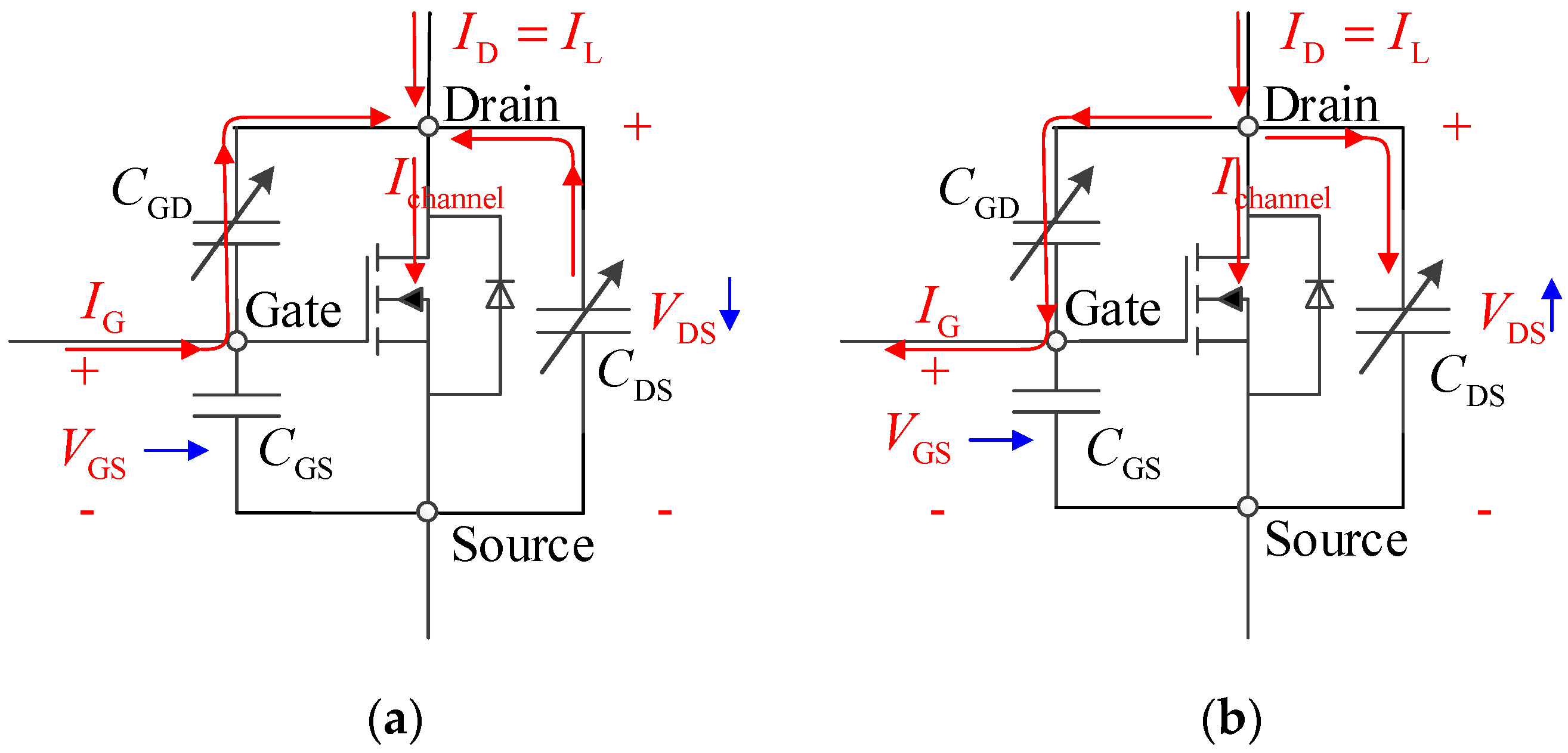
Figure 1 shows the typical structure of a SiC MOSFET consisting of three electrodes, namely drain, gate, and source, gate oxide, JFET region, and N-drift. It is a vertical device with a planar gate. Apart from that, the equivalent circuit of SiC MOSFET is also shown, including three internal parasitic capacitances: gate–drain (CGD), gate–source (CGS), and drain–source (CDS).
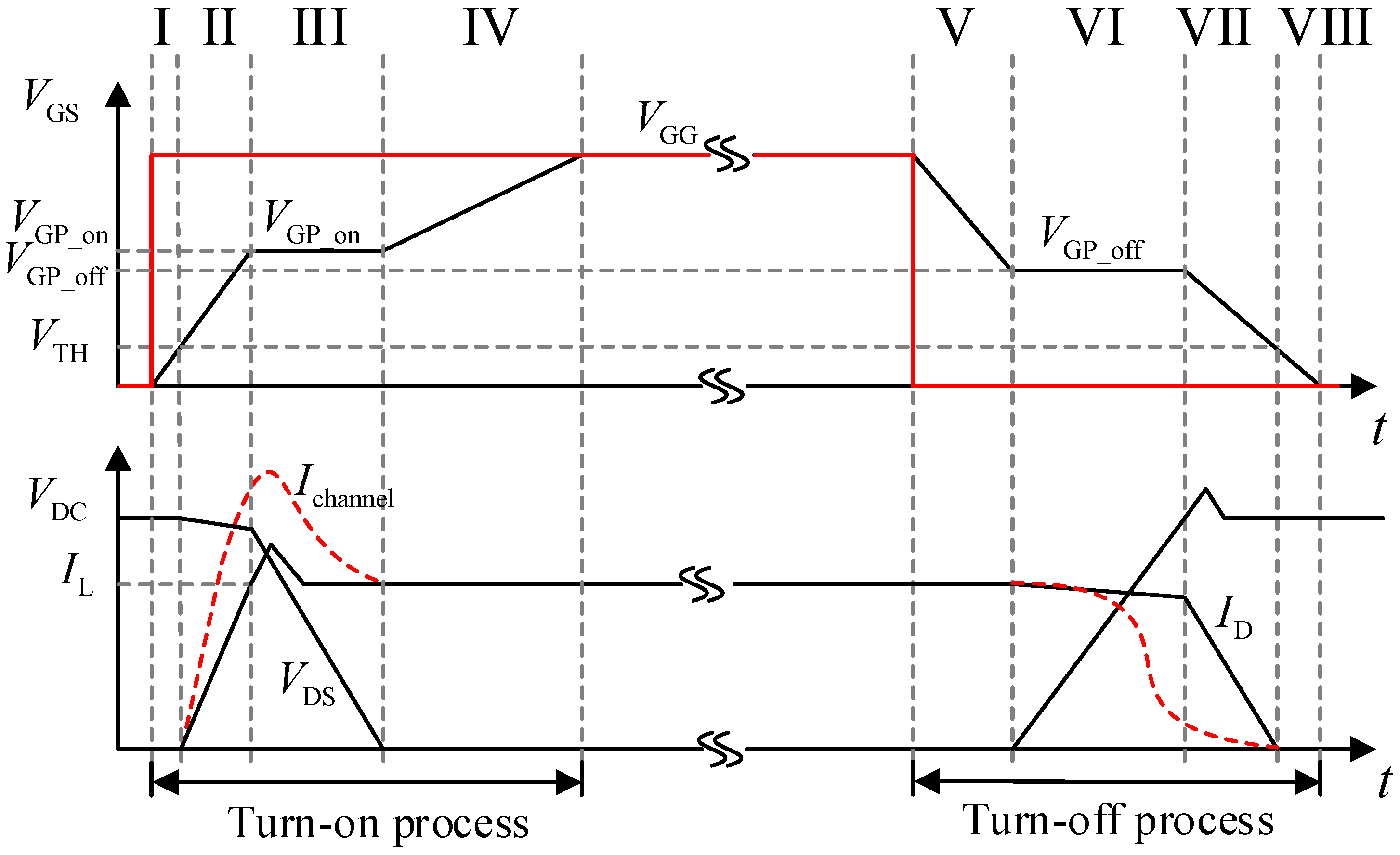
Based on an inductive load circuit, the switching characteristic of a power MOSFET is illustrated in Figure 2, showing the four phases during turn-on and turn-off. Due the existence of switching loop stray inductances, the induced voltage across stray inductances will reshape the waveforms of a drain source voltage VDS, causing a drop in turn-on and a peak in turn-off, as a result of the induced positive voltages and negative voltages, respectively [17].
The current distribution in the device is changed due to the effect of the drain–source capacitance CDS of the SiC MOSFET, which usually cannot be observed outside the SiC MOSFET. During the turn-on process, the energy stored in CDS discharges through MOS channel, which causes the channel current Ichannel to be larger than the drain current ID measured outside. While at turn-off, the capacitance CDS is charged as the drain-source voltage VDS rises. In this process, a part of the load current flows to CDS, which causes Ichannel to be smaller than ID. As a result, the gate-source plateau voltage VGP in turn-on is higher than that in turn-off.
2.2. Temperature-Based dVDS/dt Model
The dynamic behavior of SiC MOSFETs is strongly dependent on their terminal capacitances: CGD, CGS and CDS. The capacitances CGD and CGS govern the switching transient since they are charged and discharged during the turn-on and turn-off processes. The effect of capacitance CDS can’t also be neglected since it also charges and discharges. In Figure 2, the MOSFET is in the saturation region and VGS remains almost unchanged at the voltage fall period during turn-on. Consequently, the gate current deviates from the gate source capacitance CGS and the Miller capacitance CGD to mainly charge the CGD. In addition, the drain source capacitance CDS is discharged in this phase and the discharging currents will inject into the channel of the MOSFET. Similarly, the CDS is charged during the voltage rise period during turn-off, and a part of the load current will be shunt. Owing to the discharging/charging of terminal capacitances, the current flowing through MOSFET, named the channel current, is not equal to the current measured through the drain terminal, namely ID, which is larger or smaller than ID. Figure 3a shows the discharging of capacitances CGD during turn-on, whereas the charging of capacitances CGD is shown in Figure 3b. The discharging/charging process of Miller capacitance is also exhibited in this figure.
In the voltage rise phase during turn-off, the voltage across the inversion channel is higher than the saturation voltage, VDS,sat, defined as VGS − VTH, and the SiC MOSFET is in the saturation region [18,19]. The channel current is a function of saturation voltage VDS,sat and can be given as :
where B = Wμ0COX/L is the transconductance parameter, W is the channel width, L is the channel length, VTH and VGS are the threshold voltage and gate-source voltage, respectively, λ is the channel length modulation parameter, μ0 is the effective mobility of the electrons in the channel, and COX is the gate–oxide capacitor.
Since the drive voltage VGG has become the low level VGG_L in this phase, and the gate source voltage VGS reaches its Miller plateau voltage that is equal to VTH+IL/gm, the gate drive current IG can be calculated as shown in Equation (2), where RG is the gate drive resistance, IL is the load current, and gm is the device’s transconductance:
The capacitance CDS is a drain–source voltage VDS –sensitive parameter due to the variation in depletion region width of the drain–body junction with VDS, which is given by [20,21]:
where:
while q is the fundamental electronic charge, εSiC is the dielectric constant in SiC, NA is the p-well region doping, ADS is the drain–source overlap area, Vbi is the junction potential in drain-body junction, ND is the doping in drift region, and ni is the intrinsic carrier concentration of SiC.
The capacitance CGD is consisted of the gate oxide capacitance COX = εOXAGD/tox in series with the bias-dependent depletion capacitance under gate oxide CGDJ = AGD(qNAεSiC /2VDS)1/2, which is given by:
According to the charging and discharging processes of CGS, CGD, and CDS as seen in Figure 3, the variation in voltage can be calculated for the voltage rise period during turn-off:
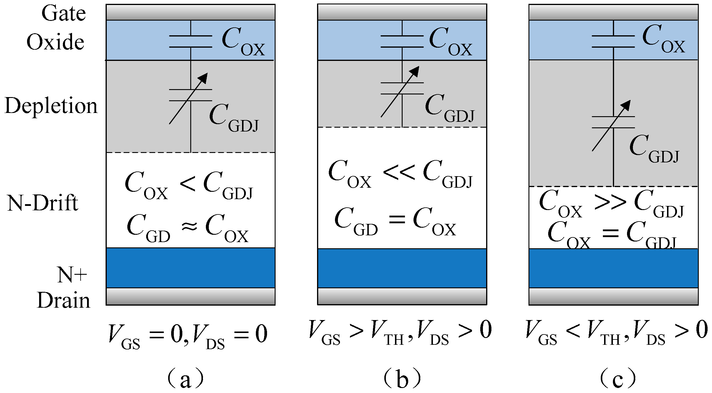
where CGS is gate-source capacitance and ID is drain current of the SiC MOSFET, which is equal to load current IL. According to different operating conditions, Mc Nutt et al. [22] found that capacitance CGD can be further simplified. Figure 4 shows how the capacitance CGD varies under different operating conditions. When gate-source voltage VGS is greater than threshold voltage, and drain-source voltage VDS is greater than zero, capacitance CGD is approximately equal to the gate oxide capacitance COX because depletion capacitance CGDJ is far in excess of the COX. Hence, Equation (6) can be further simplified by using COX instead of CGD. Additionally, during turn-on, the expression of the variation in voltage can also be derived is similar to Equation (6), where gate current is defined as IG = (VGG_H − (IL/gm + VTH))/RG.
2.3. Dependency Analysis
Equation (6) shows that the variation in voltage is dependent on temperature, since the channel current and gate current are correlated with temperature. The load current, voltage, and gate drive resistance also have some influence on variation in voltage. The relationship between channel current and temperature depends on the temperature dependency of the threshold voltage and the effective mobility in SiC MOSFET. When the surface potential of the channel in the MOSFET is exactly twice the bulk potential, the value of the gate voltage is called the threshold voltage. This means that the gate potential has induced sufficient band bending for the intrinsic Fermi level in the p-type body of the device to be below the Fermi level. The electron concentration in the channel is exactly equal to the p-body doping and the channel is properly inverted, which is the minimum gate voltage to make the device work. Hence, the threshold voltage can be calculated as shown below in Equation (7), where ψB is Fermi-potential, Qf is the fixed oxide charges, and φms is the work function difference between metal and semiconductor [23]:
with:
Due to the work-function difference φms and fixed oxide charges Qf being essentially independent of temperature, the threshold voltage temperature dependency can be given through differentiating Equation (7) with respect to temperature:
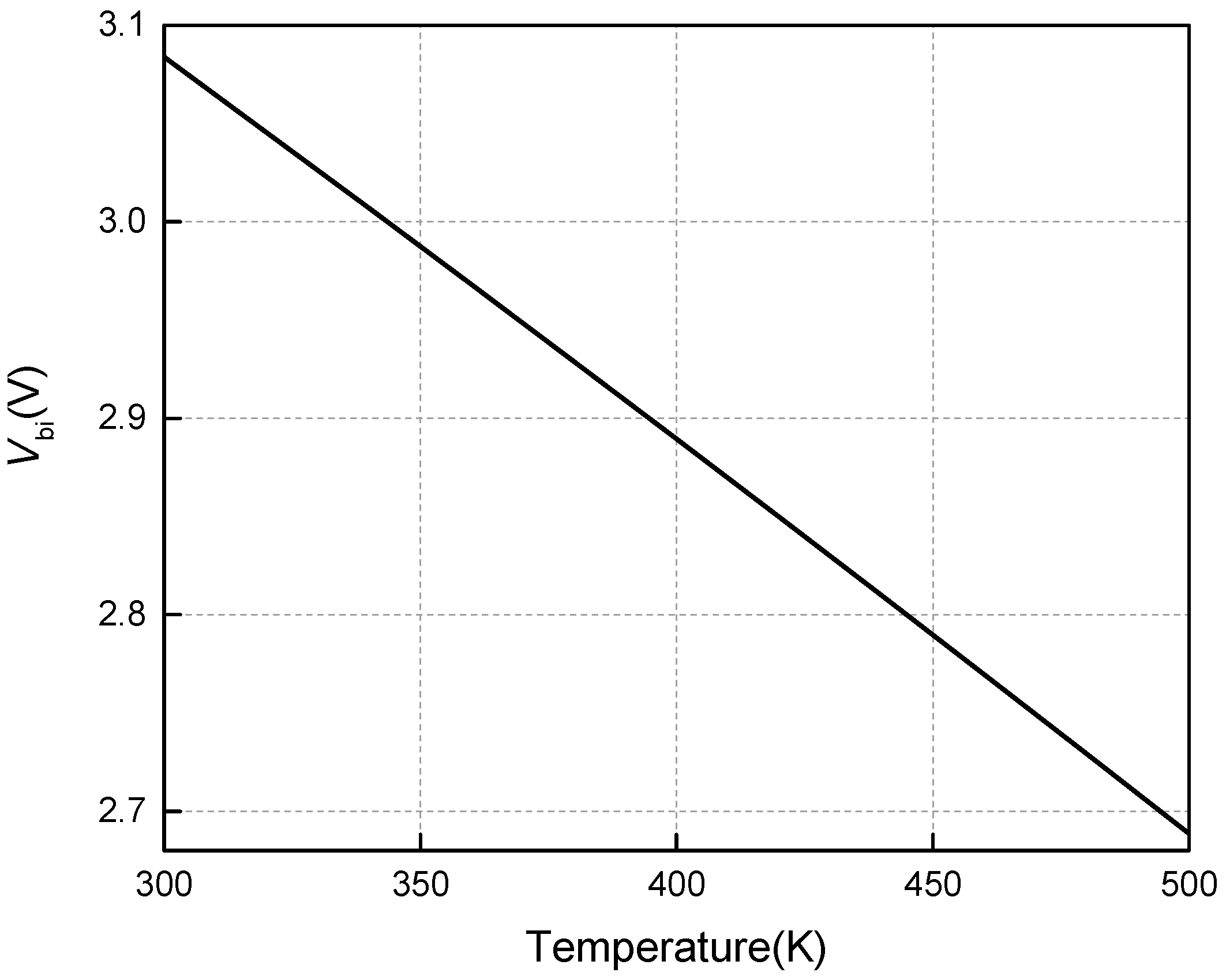
From Equation (3), assuming a constant drain-source voltage VDS, it is known that CDS varying with temperature is dominated by the temperature dependency of Vbi. In the expression of Vbi in Equation (4), as temperature T increases, kT/q rises and decreases. Hence, the more dominant parameter will determine how CDS changes with temperature. Theoretically, the term dominates the temperature dependency of CDS since Vbi decreases with temperature shown in Figure 5, where the drift region doping ND is 3.8 × 1015 cm−3. From Figure 5, CDS increases with temperature owing to its inverse proportional relationship with Vbi, according to Equation (4). As reported by Chen et al. [7], experimentally, the C-V characteristics of SiC MOSFET almost overlap under different temperatures. Hence, the temperature dependency of CDS is neglected in the following analysis. Additionally, the CGS and COX are generally considered to be constant.
From Equation (2), gate current is also correlated with threshold voltage and effective mobility, since the Miller plateau voltage is determined by the two parameters, resulting in the gate current varying under different temperatures. Hence, according to the temperature derivative of Equation (6), the temperature dependence of dVDS/dt can be obtained, as shown in Equation (10):
According to Equations (1) and (2), the temperature dependence of the channel and gate currents can be given by:
The equation of mobility can be adopted from Mudholkar et al. [22]:
Substituting Equations (9), (11) and (12) into Equation (10), the temperature sensitivity of dVDS/dt can be derived via the temperature dependency of threshold voltage and effective mobility. From Equation (13), mobility μ0 possesses a negative temperature coefficient and decreases with temperature. However, for SiC MOSFET, dμ0/dT is very low and can be neglected due to its wide band-gap characteristics as reported in Hasanuzzaman et al. [24]. Hence, the temperature sensitivity of dVDS/dt is dominated by dVTH/dT and is negative because the temperature coefficient of threshold voltage is negative. Hence, turn-off dVDS/dt decreases as temperature increases. Similarly, the variation tendency of dVDS/dt under different temperatures during the turn-on process can also be predicted.
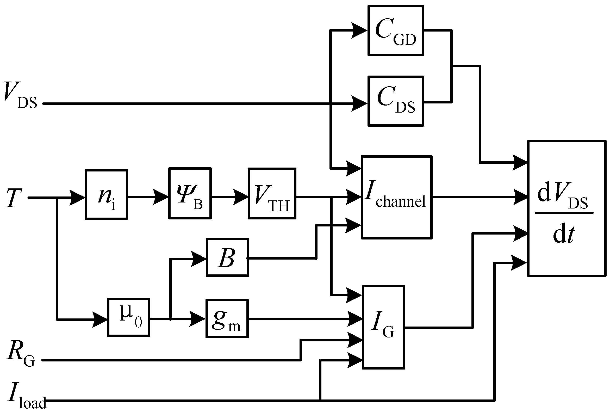
From Equation (6), the variation in voltage is also affected by load current, supply voltage, and gate drive resistance. Since the derivative of dVDS/dt with respect to the load current is positive, as shown in Equation (14), it has a positive impact on the variation in voltage, which means the variation in voltage increases with increasing load current:
For the voltage, the impact on the variation in voltage is similar to that of the load current because the capacitance CDS varies under different voltages, as described in Equation (3). As seen from Equation (2), the higher the gate resistance, the lower the gate current. Hence, the variation in voltage decreases with increasing gate resistance. Likewise, for the voltage fall period during turn-on, the variation in voltage also depends on the gate resistance, load current, voltage, and temperature, and their impacts on variation in voltage can be obtained through a similar analysis process as for turn-off. A flow diagram for the proposed temperature-based analytical model, described in function blocks, is given in Figure 6. The temperature dependency of variation in voltage is a result of the variation of the intrinsic carrier concentration ni and the effective mobility of the electrons μ0 with temperature. Owing to the positive temperature effect of the intrinsic carrier concentration ni and the negative temperature effect of effective mobility of the electrons μ0, dVDS/dt decreases with temperature for turn-off and increases for turn-on. Since SiC MOSFET has wider band-gap energy, the temperature sensitivity of the effective mobility of the electrons μ0 can be neglected and can be considered approximately constant in the model.
3. Experiment Details
The static characteristics of SiC MOSFET were measured using a B1505A curve tracer (Agilent, Santa Clara, CA, USA) with the device placed in an environment chamber to control the temperature. The switching characteristics were obtained by the clamped inductive double-pulse test circuit shown in Figure 7.
The switching waveforms were captured using a 610Zi digital oscilloscope (Lecroy, New York, NY, USA) which has a bandwidth of 1 GHz and a sample rate of 20 GS/s. During the experiment, different ambient temperatures were simulated using a heater, and the SiC MOSFET was mounted at the bottom of the test circuit board, connected to the heater through an aluminum plate with some thermal paste for reliable heat transfer, shown in Figure 8. The heater can vary the temperature from room temperature to 450 °C. Theoretically, the SiC MOSFET chip can be normal operation above 300 °C due to its wider band gap and higher thermal conductivity. However, the maximum recommended operation temperature per the device manufacturer is 175 °C, owing to the considerations listed on the packaging and reliability issues. Hence, the maximum of 175 °C was selected for experimental measurements. A fan was used for the heat dissipation of the test circuit board to reduce the effects of temperature on the other components. In the test, the SiC MOSFET and diode were SCT2080KE (Rohm, Kyoto, Japan) and SCS220AM (Rohm, Kyoto, Japan) devices, respectively.
4. Experimental Results
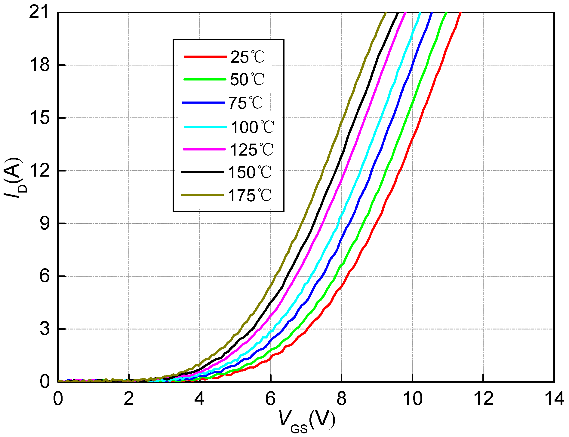
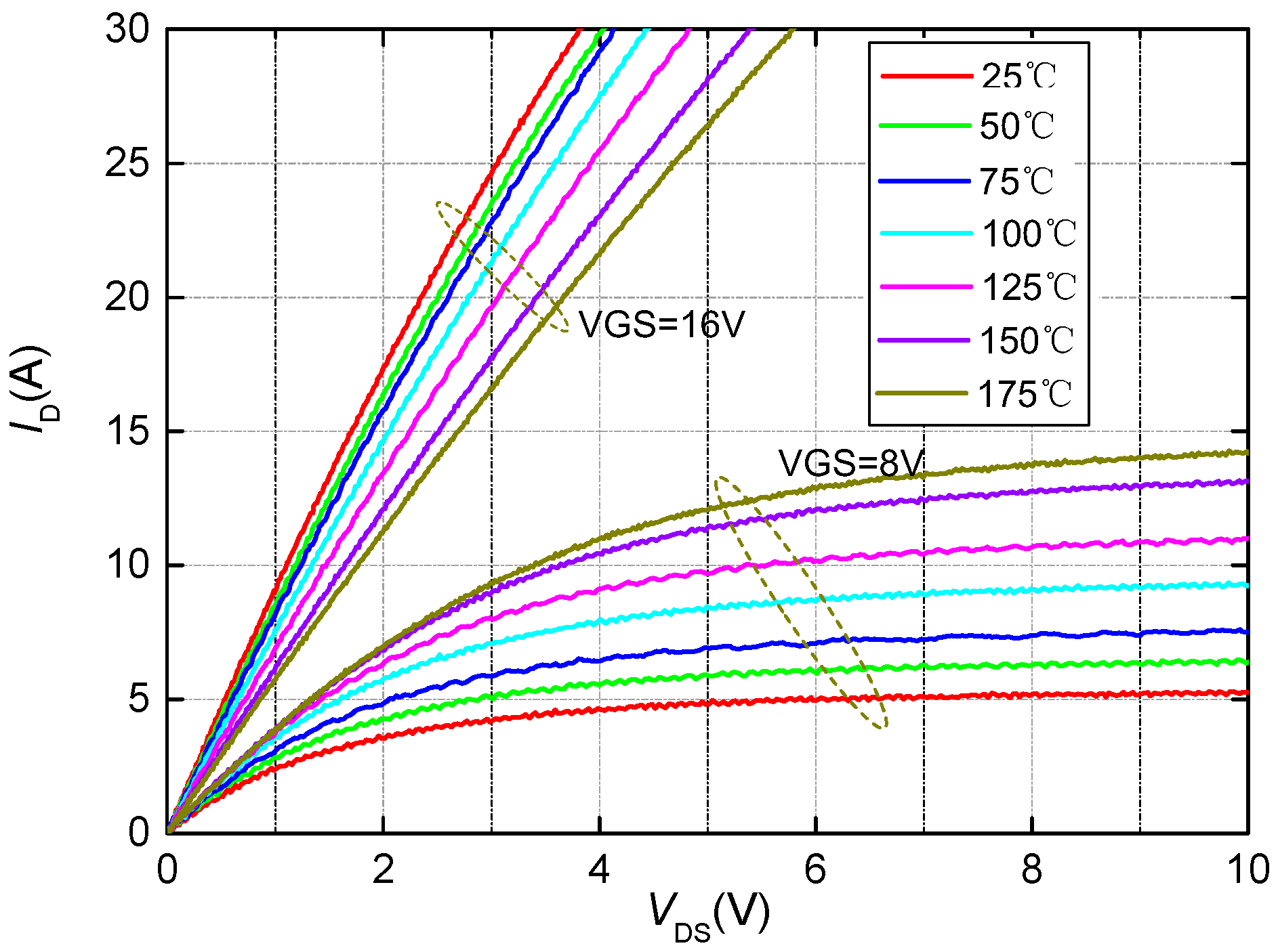
4.1. Static Characteristics under Different Temperatures
Figure 9 and Figure 10 show SiC MOSFET transfer and output characteristics at varying temperatures, respectively. The temperature dependence of the threshold voltage was obtained, as shown in Figure 11. The square represents the tested values under different temperatures, the solid line represents the fitted values, and the dashed line is representative of the calculation based on Equation (7). As seen, the threshold voltage significantly decreases with temperature increase, which is typical for 4H-SiC MOSFETs and has been observed in previous studies [13,14]. The effect is caused by the increase of intrinsic carrier concentration at higher temperature, seen in Equation (7), due to increased thermal generation of carriers across the band gap, which forms the channel easier.
From Figure 11, the temperature dependency of threshold voltage is approximately linear. The temperature sensitivity coefficient kVT is about −6.37 mV/°C. If nominal threshold voltage VTH0 at room temperature is known, a simple expression can be used to describe threshold voltage at any measured temperature T:
Figure 11 also shows the calculated values of threshold voltage according to Equation (7). Reasonably good agreement exists between calculations and measurements. Nevertheless, the analytical model of threshold voltage, given by Equation (7), is often used for theoretical analysis since its parameters relate to the physics of the device. These parameters are usually hard to obtain. The linear fitting expression of the threshold voltage, given by Equation (15), is usually adopted in practical applications. In order to simplify the calculation, Equation (15) is used for the following calculations. The temperature dependency of transconductance gm is dominated by the effective mobility μ0. As aforementioned analysis, the dμ0/dT of SiC MOSFET is very low and can be neglected due to its wide band-gap characteristics. Hence, the temperature dependency of transconductance gm is also not considered.
4.2. Temperature Dependency of dVDS/dt
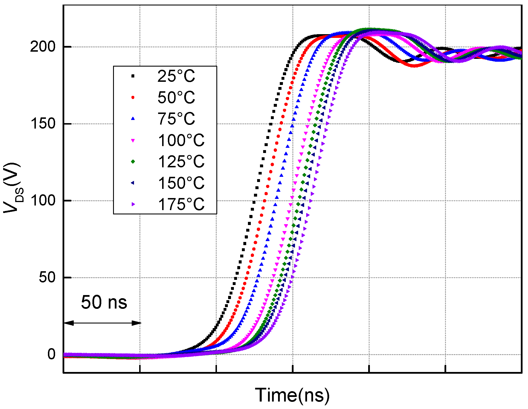
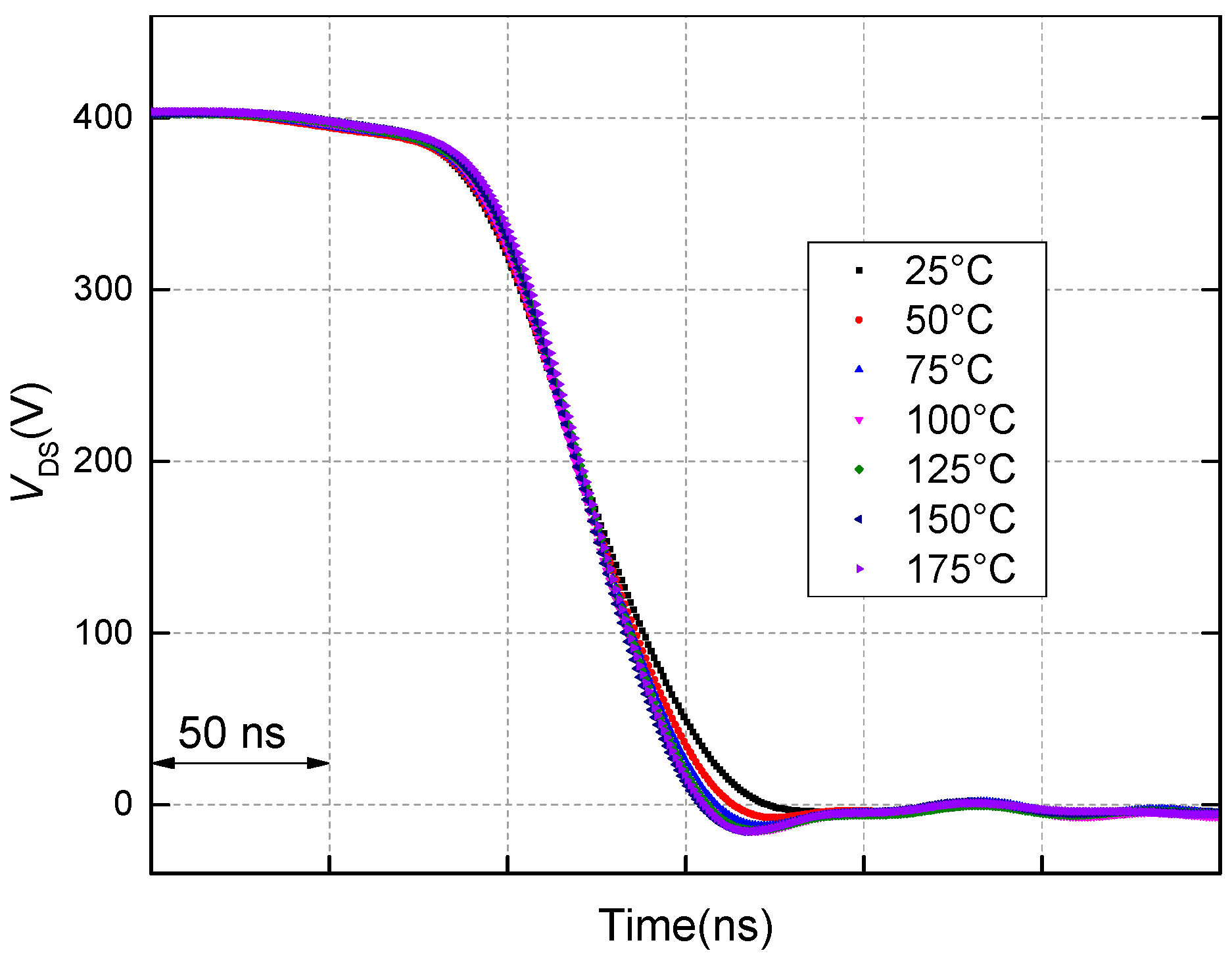
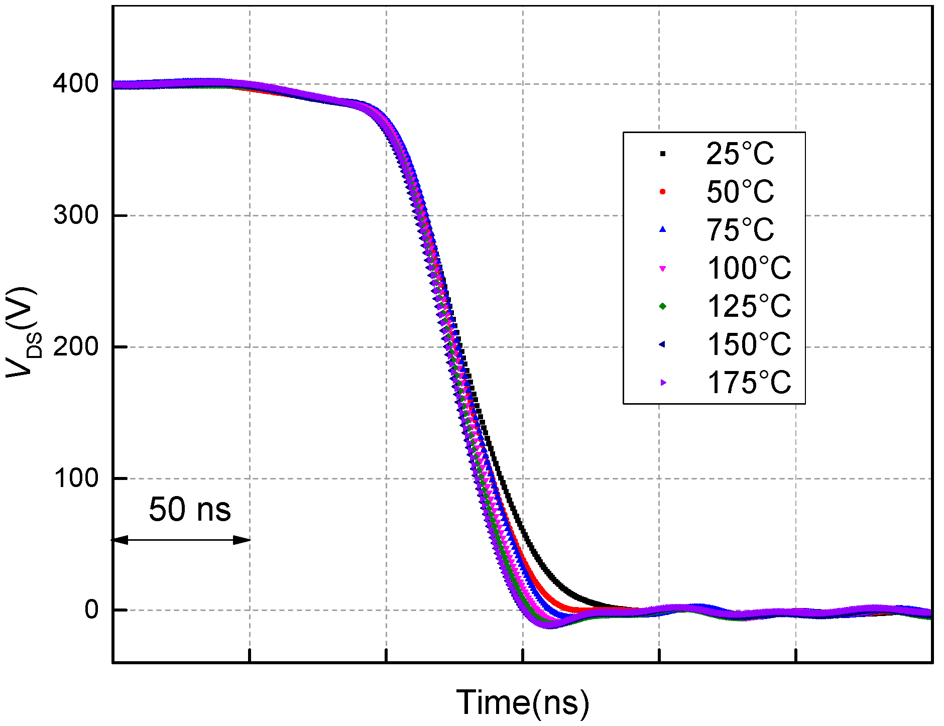
From Equation (6), dVDS/dt depends on device temperature, load current, gate resistors, and voltage. Here, the effects of these factors are investigated and the results are shown in Figure 12, Figure 13, Figure 14, Figure 15, Figure 16, Figure 17, Figure 18 and Figure 19, where the turn-off waveforms of drain voltage are shown in Figure 12, Figure 13, Figure 14 and Figure 15, and the turn-on waveforms are shown in Figure 16, Figure 17, Figure 18 and Figure 19. The test conditions were set to voltages of 200, 400 and 600 V, and load currents of 10, 15 and 20 A. The gate resistor varied from 10 Ω to 150 Ω and the temperature ranged from 25 °C to 175 °C. An external drive system with 24/–5 voltage was used in the test and a double pulse signal was generated by a pulse generator. The current was measured using a Pearson current sensor. As seen, load current, voltage, temperature, and gate resistor have different impacts on dVDS/dt during turn-off and turn-on. During turn-off, the relationship between dVDS/dt and temperature is strongly dependent on the gate resistor. With larger values for the gate resistor, the curves nearly overlap under different temperatures. With smaller values for the gate resistor, the variation in voltage barely changed as temperature increased. However, the time at which the voltage rose obviously increased with temperature, which means the delay time varied as temperature increased.
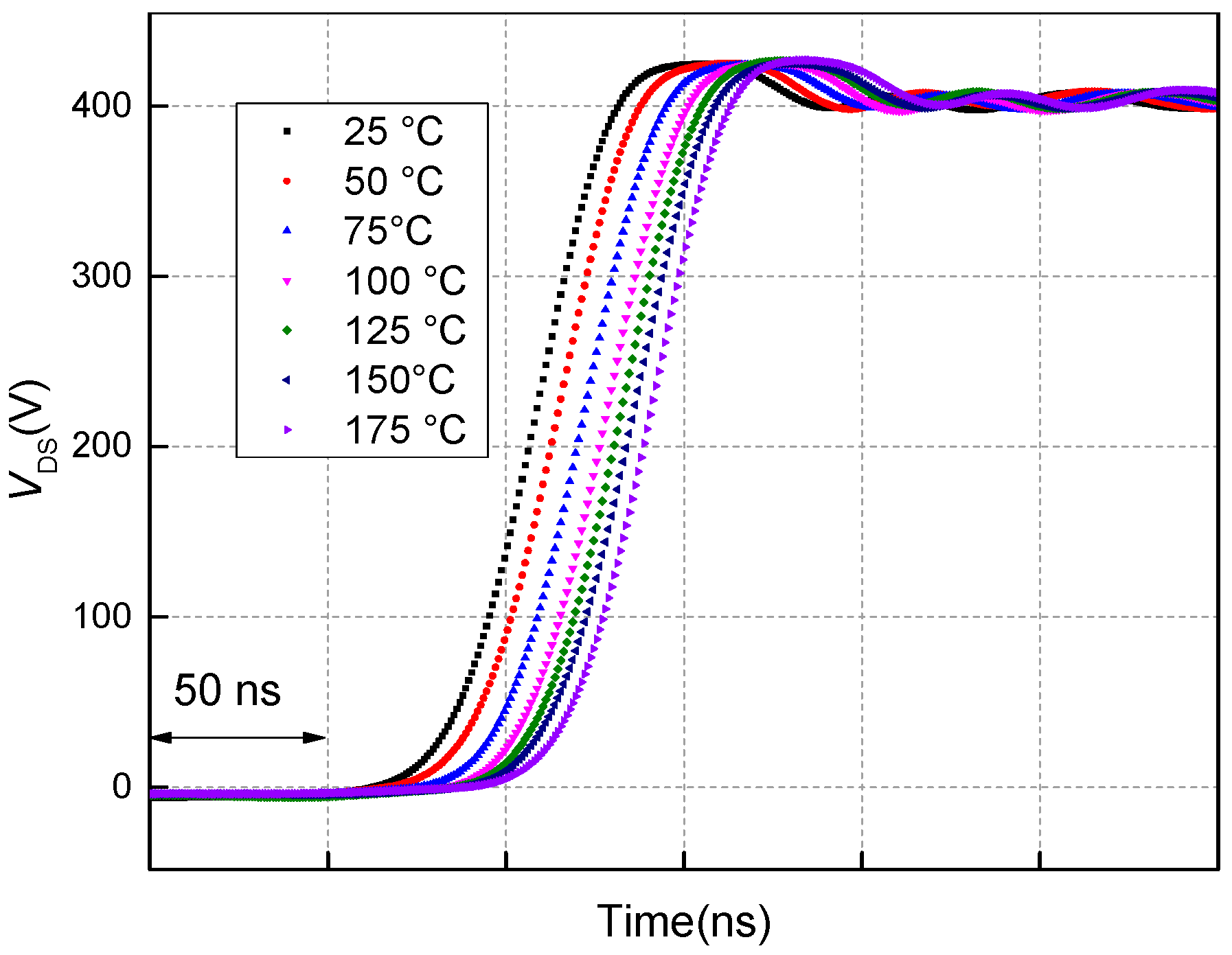
In the voltage fall period during turn-on, at larger gate resistor values, the impact of temperature on the variation in voltage is obvious and its magnitudes increased as temperature increased. The time at which the voltage falls is different, and decreased with temperature. For smaller gate resistor values, the variation in voltage was nearly the same under different temperatures, since the waveforms overlapped. Moreover, load current and voltage were also important factors for the variation in voltage with temperature.
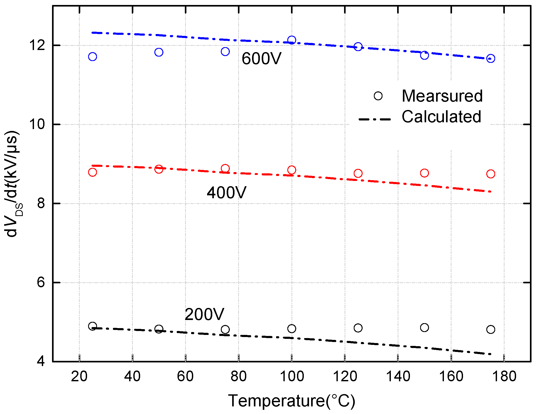
From the above curves, the measured values of dVDS/dt, which varies with temperature under different measurement conditions, were obtained. The results are shown from Figure 20, Figure 21, Figure 22, Figure 23, Figure 24 and Figure 25, where Figure 20, Figure 21 and Figure 22 are the results for turn-off, and Figure 23, Figure 24 and Figure 25 are for turn-on. The calculated values are also shown in these figures. In the calculations, the values of CGS and COX are 2.192 nF and 3.387 nF, respectively, extracted by a constant gate current circuit during turn-on. Indeed, for a SiC MOSFET the relative change in channel length is very small comparing with the long channel, λ can be treated as zero. According to some points in the device output characteristic saturation region, the values of W and L were obtained. The drain–source overlap area ADS was 5.3676 mm2. Equation (15) was adopted as the expression of threshold voltage under different temperatures.
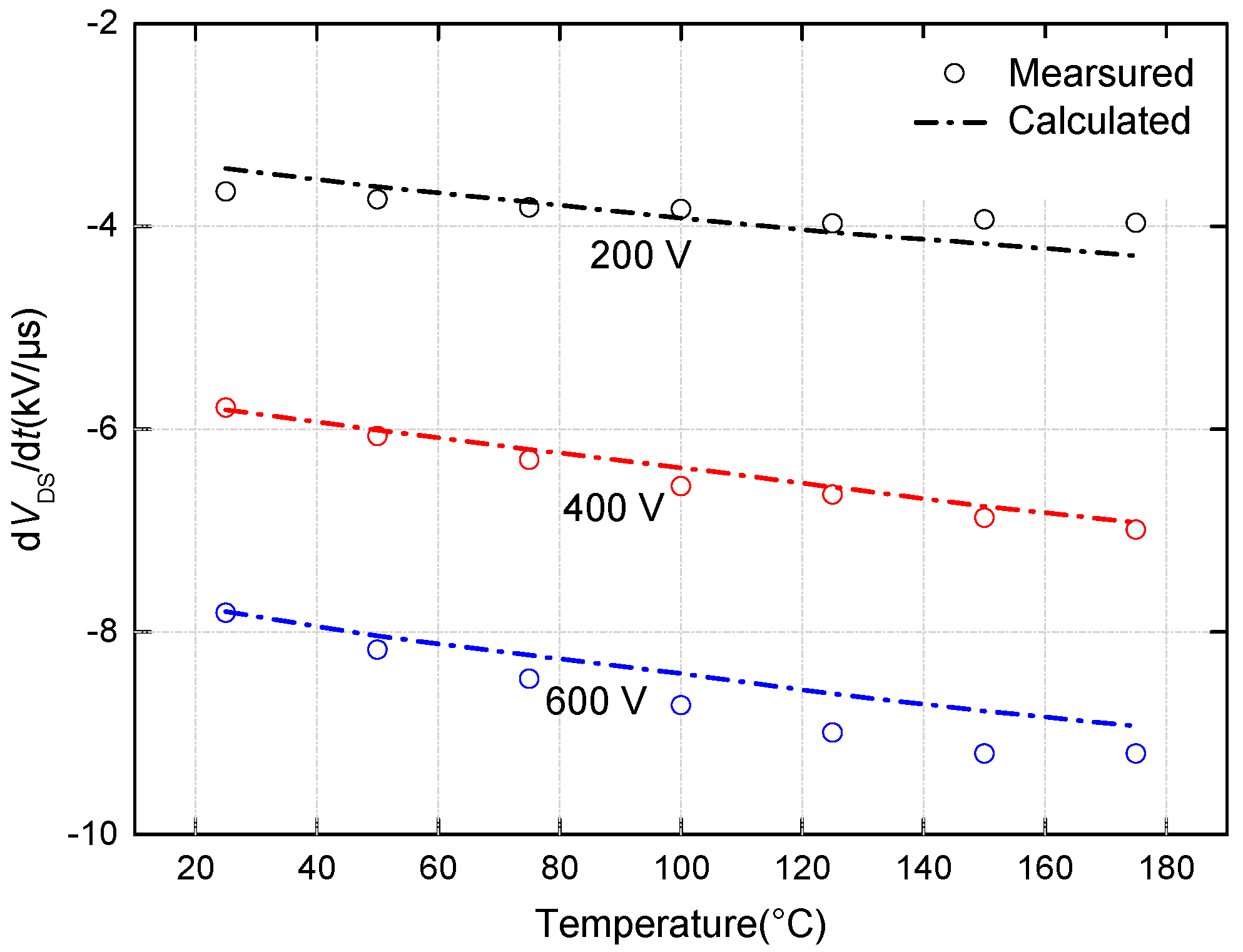
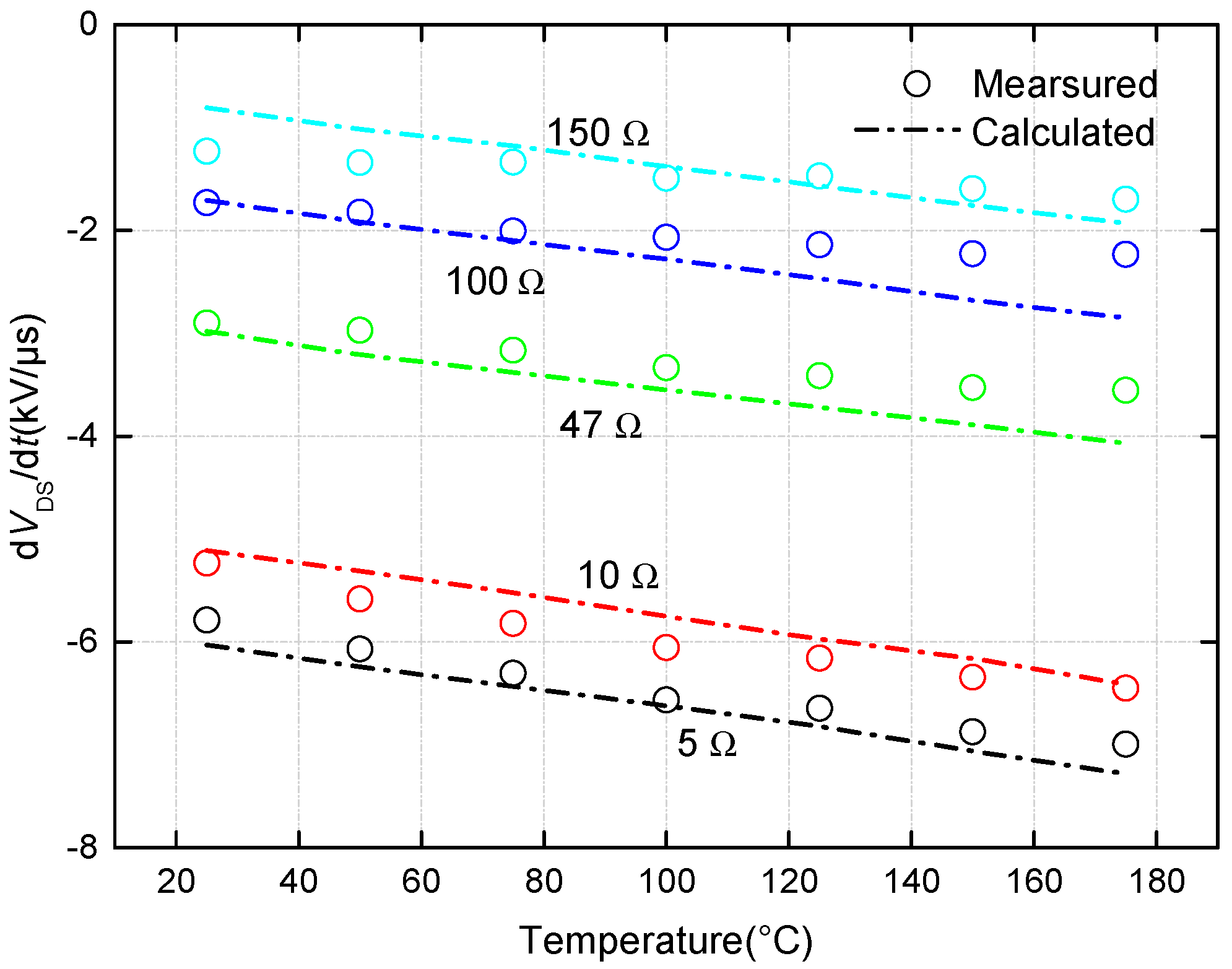
For a fixed voltage of 400 V and gate resistance of 10 Ω, the relationship between dVDS/dt and temperature under different load currents is presented in Figure 20. Figure 21 shows the temperature dependence of dVDS/dt under different voltages at 15 A load current of and 10 Ω gate resistance. Note that dVDS/dt has little fluctuation as the temperature increases, meaning that turn-off dVDS/dt is not a strong function of temperature. The dVDS/dt also increases with load current and supply voltage. The positive voltage coefficient of dVDS/dt is due to the fact that drain-source capacitance and Miller capacitance reduce with increasing supply voltage. The Miller capacitance is consisted of a fixed oxide capacitance and a depletion capacitance that varies with voltage. The depletion width increases as voltage increases resulting in a small depletion capacitance and hence the Miller capacitance declines at a large voltage. While, drain-source capacitance is comprised of the depletion region capacitance of drain-body junction and the region width also increases with voltage. Hence drain-source capacitance decreases. The calculated results show dVDS/dt is minimally temperature sensitive and decreases with temperature. Some discrepancies can be found between the measurements and calculations. The reason for this may be the temperature dependence of the effective mobility compensating for the temperature dependence of the threshold voltage in realistic experimental conditions. Furthermore, the impact of the gate resistors on the temperature dependence of dVDS/dt was also measured at 400 V and 15 A. The results are exhibited in Figure 22. The dVDS/dt varied with different resistors, and was large with smaller resistor values and was small with larger resistor values. The reason results from the variation of gate current at different resistors observed in aforementioned analysis.
During the period of voltage fall during turn-on, the relationship between dVDS/dt and temperature, under different load currents, at 400 V and 10 Ω, is presented in Figure 23. For different voltages, the relationship at 15 A and 10 Ω is shown in Figure 24. Notably, dVDS/dt is less than zero and its magnitude increases with temperature, as expected. Moreover, the temperature dependency of dVDS/dt exhibits near-linear characteristics. The results are interesting since the monotonic relationship may be a potential indictor for junction potential measurement for SiC MOSFET. At the same temperature, a larger load current results in a smaller dVDS/dt. For voltage, the magnitude of dVDS/dt is larger for a larger voltage. To evaluate the effects of gate resistors on the temperature dependency of turn-on dVDS/dt, the temperature dependency of turn-on dVDS/dt was measured at 400 V and 15 A under different gate resistor values. The results are shown in Figure 25. A variation in dVDS/dt can be observed in Figure 25 for different gate resistors at the same temperature. A smaller gate resistor results in a larger magnitude of dVDS/dt. Moreover, in the above figures, the calculated and measured values show good agreement at the evaluated temperature range.
5. Discussion
The variation trend between dVDS/dt and temperature for SiC MOSFET can be also seen in previous studies. In Chen et al. [9] and DiMarino et al. [14], the measurements were performed at a supply voltage of 600 V and load current of 10 A with 10 Ω gate resistance. The impact of temperature is clear and the magnitude of dVDS/dt decreases as temperature increases for turn-off, but increases with increasing temperature for turn-on. Othman et al. [11] experimentally showed the temperature-sensitivity of turn-off dVDS/dt is very low and approximately constant under 400 V, 15 A, and 28 Ω gate resistance test conditions. When temperature ranges from 25 °C up to 175 °C, the value of dVDS/dt is approximately 10.44 V/ns. However, for turn-on dVDS/dt, the magnitude increases from 4.6 V/ns at 25 °C to 6.62 V/ns at 175 °C. As reported by Takao et al. [12], the same conclusions were drawn from the switching waveforms of SiC MOSFETs at 25 °C and 175 °C at 600 V, 10 A, with 11.36 Ω gate resistance. The magnitude of turn-on dVDS/dt is approximately 12 V/ns at 25 °C and 15 V/ns for 175 °C, whereas the values of turn-off dVDS/dt are all approximately 29.11 V/ns for both 25 °C and 175 °C. These provide a potential solution for SiC MOSFET junction temperature estimation.
In the case of Si IGBTs, the turn-off dVCE/dt under different temperatures has been reported by Bryant et al. [25]. The dVCE/dt possesses a negative temperature coefficient and decreases with temperature decreases. For different load currents, the slope is the same and its value is 6.75 V/(μs°C). Because of this fixed sensitivity and linearity, turn-off dVCE/dt can be used as an effective indicator for junction temperature measurement of an IGBT. However, for a SiC MOSFET, turn-off dVDS/dt is not strongly correlated with temperature. Hence, monitoring turn-off dVDS/dt seems to be infeasible for junction temperature measurement of a SiC MOSFET.
Equation (10) shows the two temperature-sensitive parameters that dominate the temperature dependency of dVDS/dt are the threshold voltage and the effective mobility. For Si MOSFET, the effective mobility decreases with temperature and its temperature dependency is negative. But for SiC MOSFETs, as reported in [24], the temperature dependency of effective mobility can be neglected and be considered approximately constant due to its wide band-gap characteristics. Hence, it can be concluded theoretically that the temperature dependency of dVDS/dt in Si MOSFETs is less than that in SiC MOSFETs owing to the compensating effects of the temperature characteristic of the effective mobility to the temperature characteristic of the threshold voltage in Si MOSFETs. However, it is hard to find the experimental measurements on the temperature dependency of dVDS/dt for Si MOSFETs in previous literature. A comprehensive comparison between Si MOSFETs and SiC MOSFETs, regarding the dependency of the dVDS/dt on temperature, load current and gate resistor, will be performed experimentally in the next step.
From the measurements, the turn–on dVDS/dt is shown to have good temperature sensitivity and is approximately linear. The results are interesting and significant because it may be a potential indicator for junction temperature measurement of a SiC MOSFET. Others factors can also effect turn-on dVDS/dt, as shown in Figure 23, Figure 24 and Figure 25, but this is not an issue. Because the type of device and system parameters, such as voltage, load current, and gate resistance, are usually fixed in practical SiC MOSFET-based applications, and turn-on dVDS/dt is only dominated by temperature. Before the turn-on dVDS/dt–based method is used for temperature assessment, the calibration curves between dVDS/dt and temperature should be drawn experimentally and used as a lookup table. Indeed, the lookup table is easily implemented by digital signal processing (DSP). The dVDS/dt can also be easily measured by a RC high-pass connected to the drain and source terminals of device from the switching waveforms. After the dVDS/dt is measured, the corresponding junction temperature can be estimated from the lookup table.
6. Conclusions
A thorough analysis of variation in voltage for SiC MOSFETs during turn-on and turn-off was completed. It can be concluded that turn on variation of voltage is a function of temperature and has near-linear dependency with temperature. The relationship between turn-off variations in voltage and temperature was also investigated. Turn-off variation in voltage was approximately invariant with temperature with fixed supply voltage, load current, and gate resistance test conditions. Using a temperature-based analytical model for variations in voltage, we demonstrated that the temperature dependency of variation in voltage results from the positive temperature dependency of the intrinsic carrier concentration and negative temperature dependency of the effective mobility of the electrons in SiC MOSFETs. The analytical model also demonstrated the ability to correctly predict how variation in voltage varies with temperature. Additionally, the effects of supply voltage, load current, and gate resistance on the temperature dependency of variations in voltage were discussed. Due to good linearity, turn on variation in voltage may be considered as a practical temperature-sensitive electrical parameter for junction temperature estimation in SiC MOSFETs. With a database of turn-on variations in voltage with temperature, supply voltage, load current, and gate resistance, the junction temperature of SiC MOSFETs can be derived from the calibration curve. Future work includes a thorough comparison with other models, a verification of whether the turn-on variation in the voltage–based temperature measurement method represents correctly the junction temperature at realistic operation conditions, and a comprehensive assessment in terms of selectivity, linearity, generality, and possibility for online measurement.
Acknowledgments
This research work is supported by the Fundamental Research Funds for the Central Universities (106112016CDJZR158802), Graduate scientific research and innovation foundation of Chongqing, China(CYB16020), National Natural Science Foundation of China (51377184, 51607016), and Chongqing Scientific &Technological Talents Program (KJXX2017009).
Author Contributions
Hui Li and Xinglin Liao put forward to the main idea and designed the entire structure of this paper. Yaogang Hu made some suggestions in the article writing. Zhangjian Huang and Kun Wang provided some help in the experiments.
Conflicts of Interest
The authors declare no conflicts of interest.
References
- Hudgins, J. Power electronic devices in the future. IEEE J. Emerg. Sel. Top. Power Electron. 2013, 1, 11–17. [Google Scholar] [CrossRef]
- Jiang, D.; Burgos, R.; Wang, F.; Boroyevich, D. Temperature dependent characteristics of SiC devices: Performance evaluation and loss calculation. IEEE Trans. Power Electron. 2012, 27, 1013–1024. [Google Scholar] [CrossRef]
- Millan, J.; Godignon, P.; Perpina, X.; Perez-Tomas, A.; Rebollo, J. A survey of wide bandgap power semiconductor devices. IEEE Trans. Power Electron. 2014, 29, 2155–2163. [Google Scholar] [CrossRef]
- Zhu, P.; Wang, L.; Ruan, L.G.; Zhang, J.F. Temperature Effects on Performance of SiC Power Transistors (SiC JFET and SiC MOSFET). In Proceedings of the 2015 IEEE European Conference on Power Electronics and Applications (EPE’15 ECCE-Europe), Geneva, Switzerland, 8–10 September 2015; pp. 449–454. [Google Scholar]
- Lelis, A.J.; Habersat, D.; Green, R.; Ogunniyi, A.; Gurfinkel, M.; Suehle, J.; Goldsman, N. Time dependence of bias-stress-induced SiC MOSFET threshold voltage instability measurements. IEEE Trans. Power Electron. 2008, 55, 1835–1840. [Google Scholar] [CrossRef]
- Gurfinkel, M.; Xiong, H.D.; Cheung, K.P.; Suehle, J.S.; Bernstein, J.B.; Shapira, Y.; Lelis, A.J.; Habersat, D.; Goldsman, N. Characterization of transient gate oxide trapping in SiC MOSFETs using fast I-V techniques. IEEE Trans. Power Electron. 2008, 55, 2004–2012. [Google Scholar] [CrossRef]
- Chen, Z.; Boroyevich, D.; Burgos, R.; Wang, F. Characterization and modeling of 1.2 kV, 20 A SiC MOSFETs. In Proceedings of the 2009 IEEE Energy Conversion Congress and Exposition (ECCE), San Jose, CA, USA, 20–24 September 2009; pp. 1480–1487. [Google Scholar]
- Hull, B.; Das, M.; Husna, F.; Callanan, R.; Agarwal, A.; Palmour, J. 20 A, 1200 V 4H-SiC DMOSFETs for Energy Conversion Systems. In Proceedings of the 2009 IEEE Energy Conversion Congress and Exposition (ECCE), San Jose, CA, USA, 20–24 September 2009; pp. 112–119. [Google Scholar]
- Chen, Z.; Yao, Y.Y.; Danilovic, M.; Boroyevich, D. Performance Evaluation of SiC Power MOSFETs for High-Temperature Applications. In Proceedings of the 2012 IEEE Power Electronics and Motion Control Conference (EPE/PEMC), Novi Sad, Serbia, 4–5 September 2012; pp. DS1a.8-1–DS1a.8-9. [Google Scholar]
- Chen, Z.; Yao, Y.Y.; Boroyevich, D.; Ngo, K.D.T.; Mattavelli, P.; Rajashekara, K. A 1200-V, 60-A SiC MOSFET Multichip Phase-Leg Module for High-Temperature, High-Frequency Applications. IEEE Trans. Power Electron. 2014, 29, 2307–2320. [Google Scholar] [CrossRef]
- Othman, D.; Berkani, M.; Lefebvre, S.; Ibrahim, A.; Khatir, Z.; Bouzourene, A. Comparison study on performances and robustness between SiC MOSFET & JFET devices—Abilities for aeronautics application. Microelectron. Reliab. 2012, 52, 1859–1864. [Google Scholar]
- Takao, K.; Harada, S.; Shinohe, T.; Ohashi, H. Performance evaluation of all SiC power converters for realizing high power density of 50 W/cm3. In Proceedings of the 2010 IEEE International Power Electronics Conference (IPEC), Sapporo, Japan, 21–24 June 2010; pp. 2128–2134. [Google Scholar]
- Cui, Y.T.; Chinthavali, M.; Tolbert, L.M. Temperature Dependent Pspice Model of Silicon Carbide Power MOSFET. In Proceedings of the 2012 IEEE Applied Power Electronics Conference and Exposition (APEC), Orlando, FL, USA, 5–9 February 2012; pp. 1698–1704. [Google Scholar]
- DiMarino, C.; Chen, Z.; Danilovic, M.; Boroyevich, D.; Burgos, R.; Mattavelli, P. High-Temperature Characterization and Comparison of 1.2 kV SiC Power MOSFETs. In Proceedings of the 2013 IEEE Energy Conversion Congress and Exposition (ECCE), Denver, CO, USA, 15–19 September 2013; pp. 3235–3242. [Google Scholar]
- Avenas, Y.; Dupont, L.; Khatir, Z. Temperature measurement of power semiconductor devices by thermo-sensitive electrical parameters—A review. IEEE Trans. Power Electron. 2012, 27, 2081–3092. [Google Scholar] [CrossRef]
- Sundaramoorthy, V.K.; Bianda, E.; Bloch, R.; Angelosante, D.; Nistor, I.; Riedel, G.J.; Zurfluh, F.; Knapp, G.; Heinemann, A. A study on IGBT junction temperature (Tj) online estimation using gate-emitter voltage (Vge) at turn-off. Microelectron. Reliab. 2014, 54, 2423–2431. [Google Scholar] [CrossRef]
- Wang, J.J.; Chung, H.S.-h.; Li, R.T.-h. Characterization and Experimental Assessment of the Effects of Parasitic Elements on the MOSFET Switching Performance. IEEE Trans. Power Electron. 2013, 28, 573–589. [Google Scholar] [CrossRef]
- Yin, S.; Tu, P.F.; Wang, P.; Tseng, K.J.; Qi, C.; Hu, X.L.; Zagrodnik, M.; Simanjorang, R. An Accurate Subcircuit Model of SiC Half-Bridge Module for Switching-Loss Optimization. IEEE Trans. Ind. Appl. 2017, 53, 3840–3849. [Google Scholar] [CrossRef]
- Arribas, A.P.; Shang, F.; Krishnamurthy, M.; Shenai, K. Simple and Accurate Circuit Simulation Model for SiC Power MOSFETs. IEEE Trans. Electron. Devices 2015, 62, 449–457. [Google Scholar] [CrossRef]
- Chen, K.; Zhao, Z.G.; Yuan, L.Q.; Lu, T.; He, F. The Impact of Nonlinear Junction Capacitance on Switching Transient and Its Modeling for SiC MOSFET. IEEE Trans. Electron Devices 2015, 62, 333–338. [Google Scholar] [CrossRef]
- McNutt, T.R.; Hefner, A.R.; Mantooth, H.A.; Berning, D.; Ryu, S.H. Silicon carbide power MOSFET model and parameter extraction sequence. IEEE Trans. Power Electron. 2007, 22, 353–363. [Google Scholar] [CrossRef]
- Mudholkar, M.; Ahmed, S.; Ericson, M.N.; Frank, S.S.; Britton, C.L.; Mantooth, H.A. Datasheet Driven Silicon Carbide Power MOSFET Model. IEEE Trans. Power Electron. 2014, 29, 2220–2228. [Google Scholar] [CrossRef]
- Baliga, B.J. Fundamentals of Power Semiconductor Devices; Spring-Verlag: New York, NY, USA, 2008. [Google Scholar]
- Hasanuzzaman, M.; Islam, S.K.; Tolbert, L.M.; Alam, M.T. Temperature dependency of MOSFET device characteristics in 4H- and 6H-silicon carbide (SiC). Solid-State Electron. 2004, 48, 1877–1881. [Google Scholar] [CrossRef]
- Bryant, A.; Yang, S.Y.; Mawby, P.; Xiang, D.; Ran, L.; Tavner, P.; Palmer, P.R. Investigation Into IGBT dV/dt During Turn-Off and Its Temperature Dependence. IEEE Trans. Power Electron. 2011, 26, 3019–3031. [Google Scholar] [CrossRef] [Green Version]
Figure 1.
Cross structure of a silicon carbide (SiC) metal–oxide–semiconductor field-effect transistor (MOSFET).
Figure 1.
Cross structure of a silicon carbide (SiC) metal–oxide–semiconductor field-effect transistor (MOSFET).
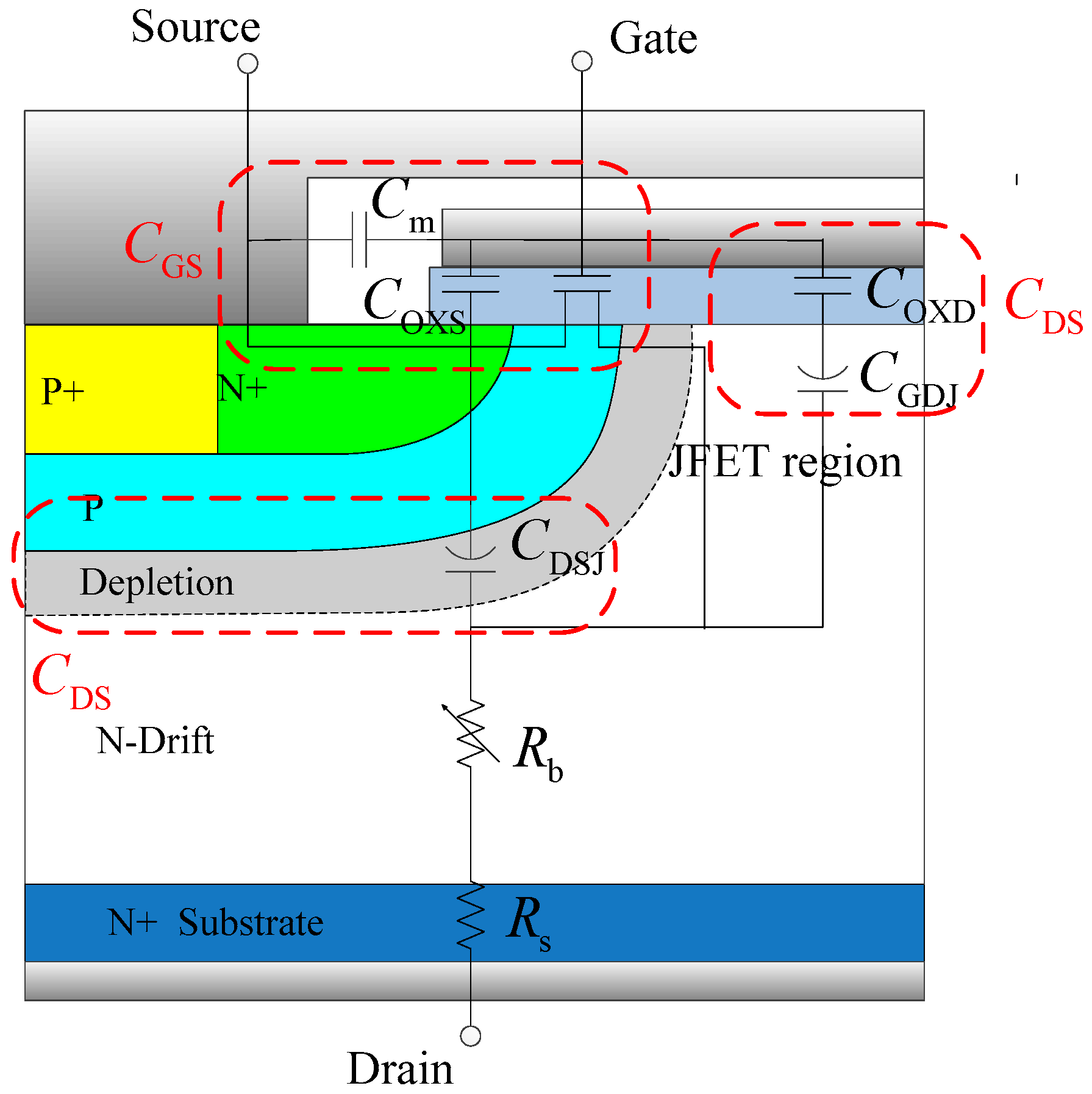
Figure 2.
Swtiching characteristic of a power MOSFET with an inductive load.

Figure 3.
Terminal capacitances charging and discharging at: (a) the voltage fall phase and (b) the rise phase.
Figure 3.
Terminal capacitances charging and discharging at: (a) the voltage fall phase and (b) the rise phase.

Figure 4.
The gate–drain capacitance (CGD) varies under different operating conditions. (a) VGS = 0, VDS = 0; (b) VGS > VTH, VDS > 0; (c) VGS < VTH, VDS > 0.
Figure 4.
The gate–drain capacitance (CGD) varies under different operating conditions. (a) VGS = 0, VDS = 0; (b) VGS > VTH, VDS > 0; (c) VGS < VTH, VDS > 0.

Figure 5.
The junction potential in drain–body junction versus temperature.

Figure 6.
Summary of dependency of dVDS/dt on operation condition.

Figure 7.
Schematics of the transient characteristics test.

Figure 8.
Schematic of the simulation of different ambient temperatures.
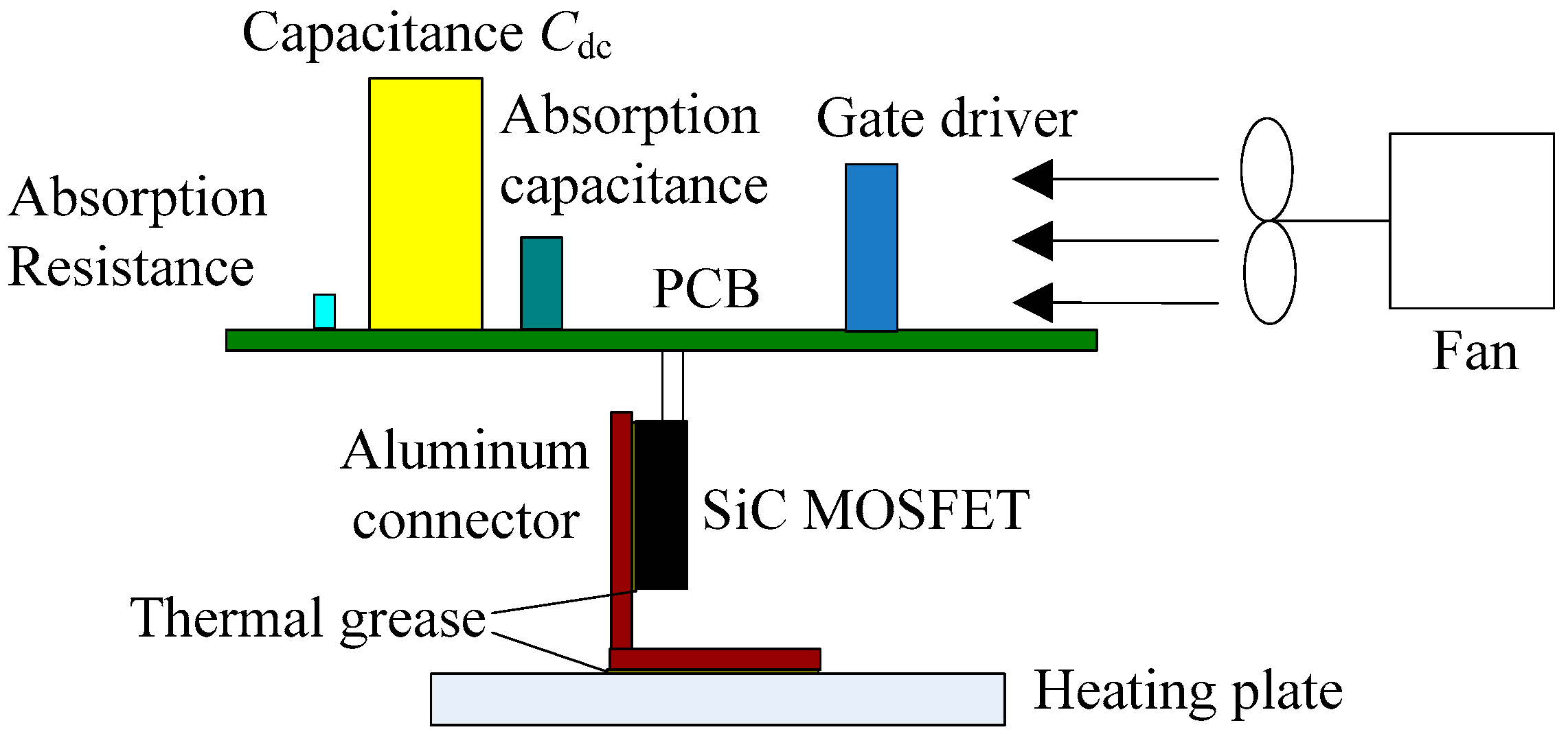
Figure 9.
Temperature-dependent transfer characteristics.

Figure 10.
Temperature-dependent output characteristics at gate-source voltages of 8 V and 16 V.

Figure 11.
Threshold voltage of SiC MOSFET under different temperatures.
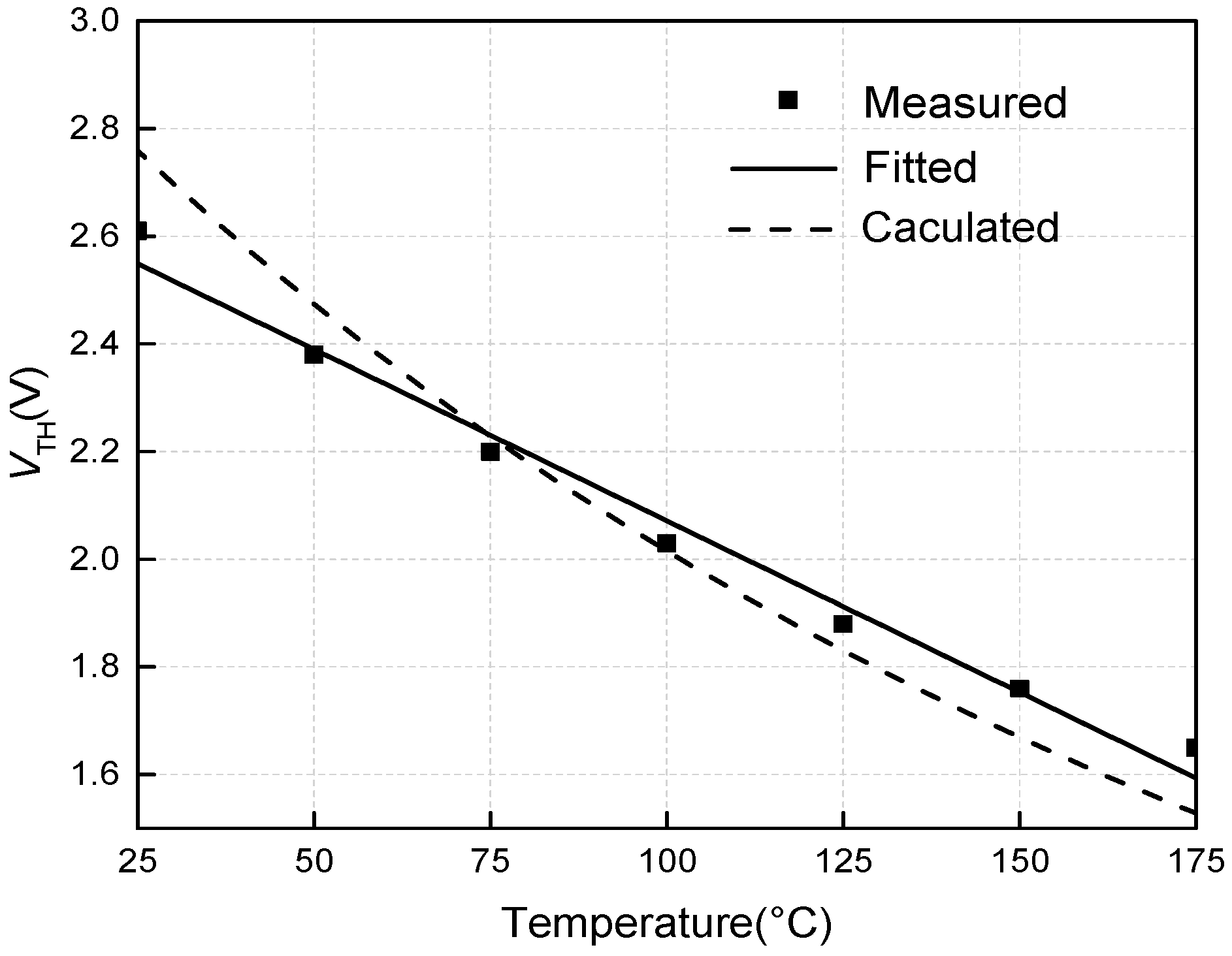
Figure 12.
Turn-off waveforms for drain-source voltage (VDS) at a voltage of 200 V, a load current 15 A, and at different temperatures with a gate drive resistance (RG) = 10 Ω.
Figure 12.
Turn-off waveforms for drain-source voltage (VDS) at a voltage of 200 V, a load current 15 A, and at different temperatures with a gate drive resistance (RG) = 10 Ω.

Figure 13.
Turn-off waveforms for VDS at a voltage of 400 V, a load current 15 A, and at different temperatures with RG = 10 Ω.
Figure 13.
Turn-off waveforms for VDS at a voltage of 400 V, a load current 15 A, and at different temperatures with RG = 10 Ω.

Figure 14.
Turn-off waveforms for VDS at a voltage of 400 V, a load current 20 A, and at different temperatures with RG = 10 Ω.
Figure 14.
Turn-off waveforms for VDS at a voltage of 400 V, a load current 20 A, and at different temperatures with RG = 10 Ω.
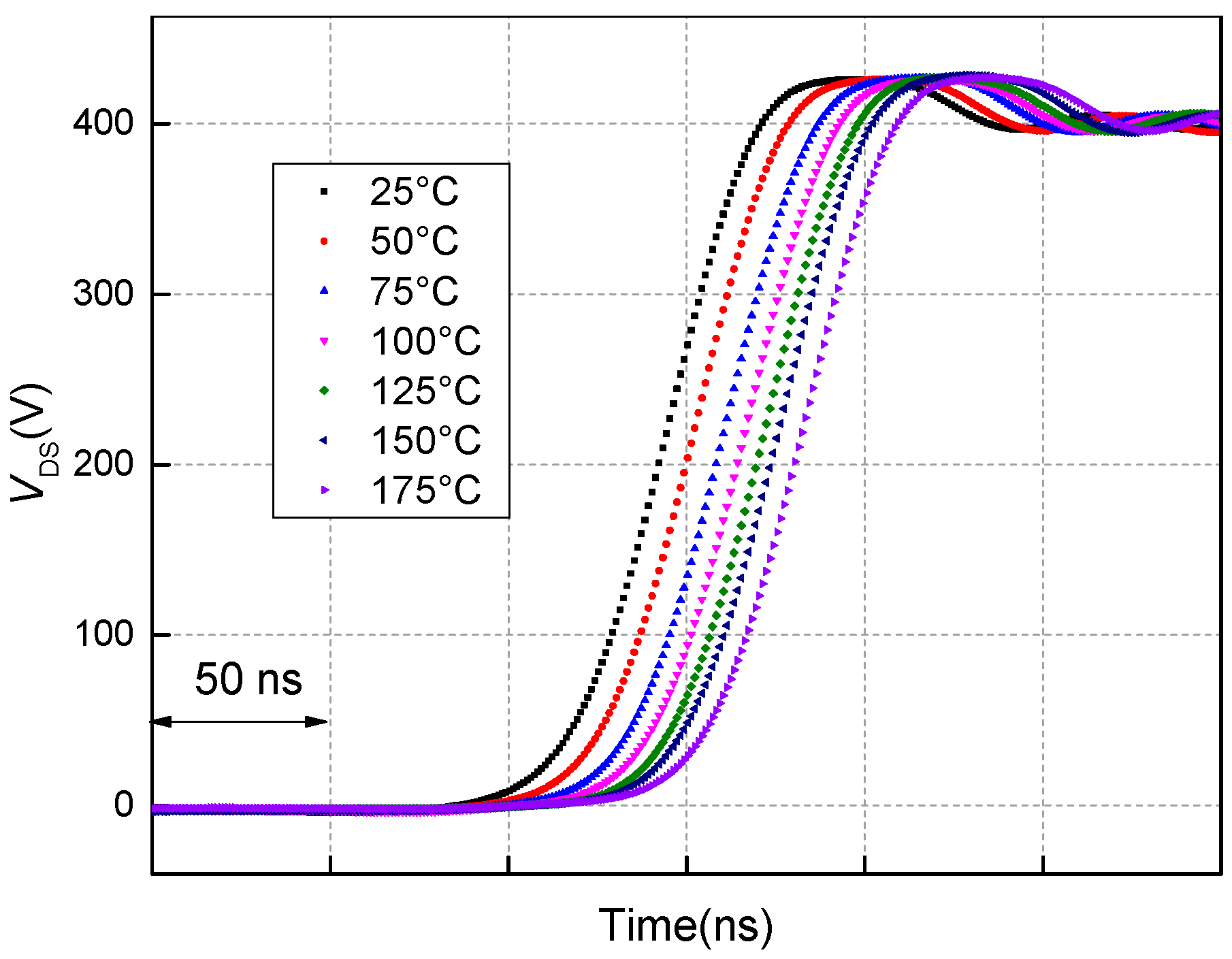
Figure 15.
Turn-off waveforms for VDS at a voltage of 400 V, a load current 20 A, and at different temperatures with RG = 150 Ω.
Figure 15.
Turn-off waveforms for VDS at a voltage of 400 V, a load current 20 A, and at different temperatures with RG = 150 Ω.

Figure 16.
Turn-on waveforms for VDS at a voltage of 200 V, a load current 15 A, and at different temperatures with RG = 10 Ω.
Figure 16.
Turn-on waveforms for VDS at a voltage of 200 V, a load current 15 A, and at different temperatures with RG = 10 Ω.
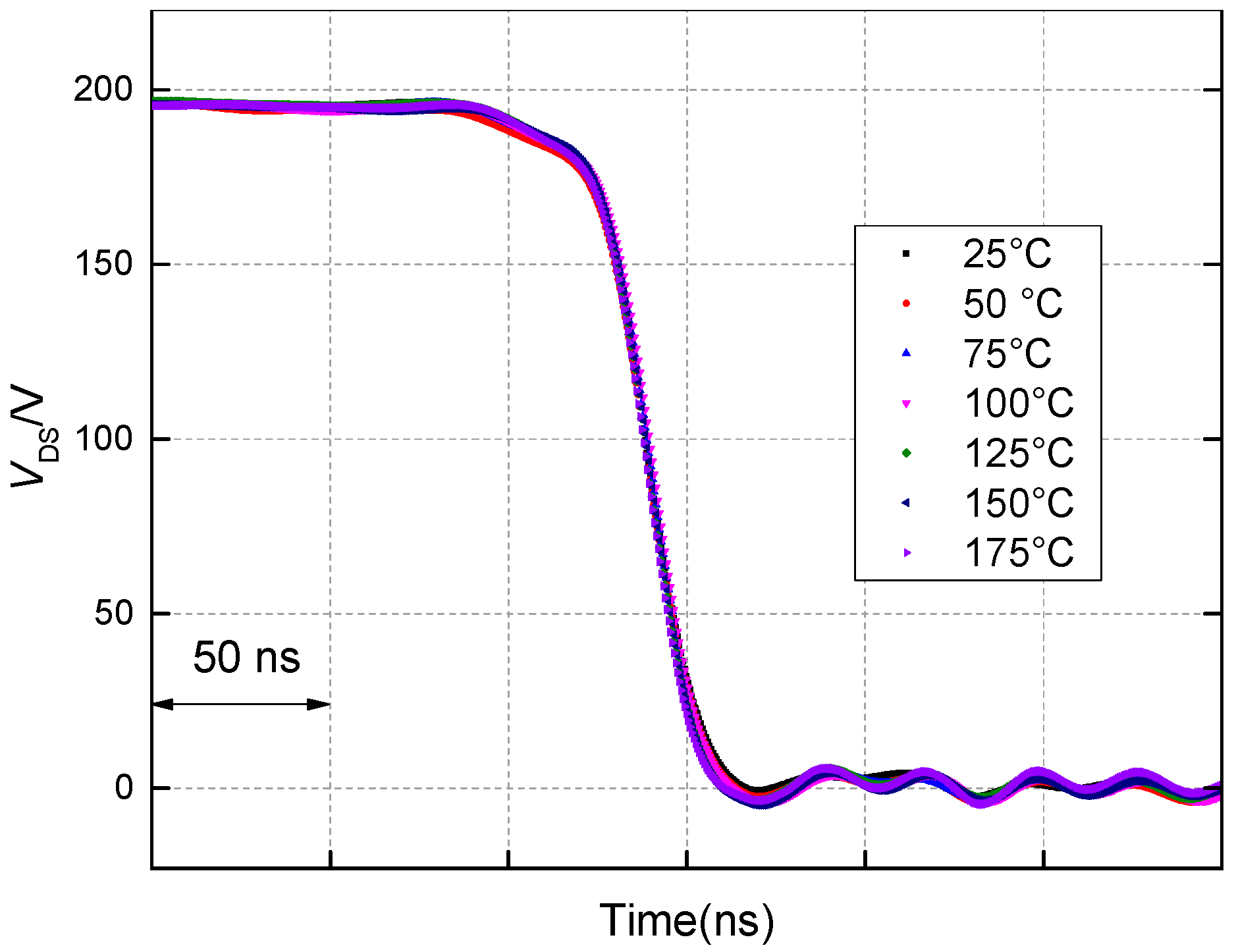
Figure 17.
Turn-on waveforms for VDS at a voltage of 400 V, a load current 15 A, and at different temperatures with RG = 10 Ω.
Figure 17.
Turn-on waveforms for VDS at a voltage of 400 V, a load current 15 A, and at different temperatures with RG = 10 Ω.

Figure 18.
Turn-on waveforms for VDS at a voltage of 400 V, a load current 20 A, and at different temperatures with RG = 10 Ω.
Figure 18.
Turn-on waveforms for VDS at a voltage of 400 V, a load current 20 A, and at different temperatures with RG = 10 Ω.

Figure 19.
Turn-on waveforms for VDS at a voltage of 400 V, a load current 20 A, and at different temperatures with RG = 150 Ω.
Figure 19.
Turn-on waveforms for VDS at a voltage of 400 V, a load current 20 A, and at different temperatures with RG = 150 Ω.
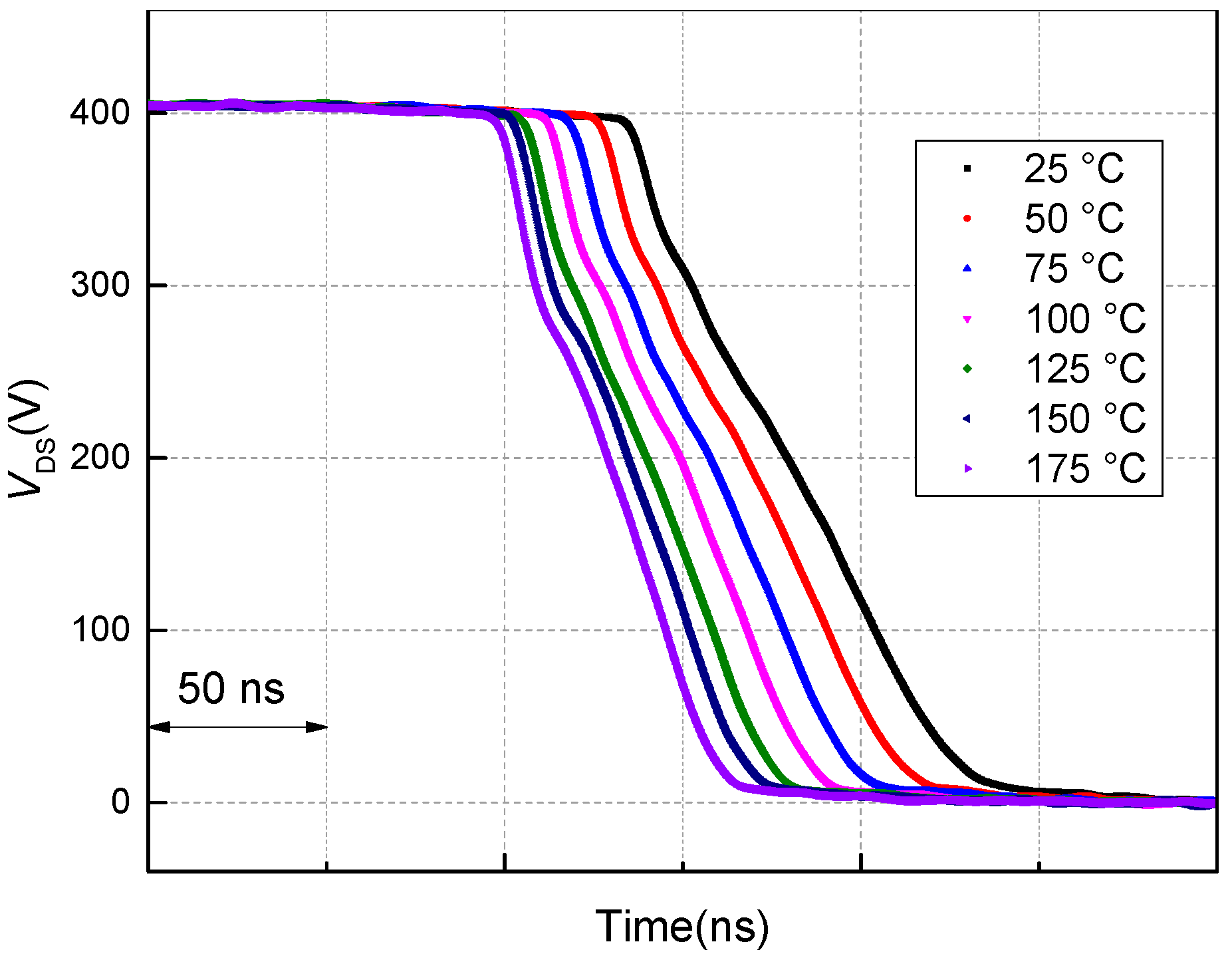
Figure 20.
Measured and calculated dVDS/dt as a function of temperature at a voltage of 400 V and a gate resistor of 10 Ω during turn-off, shown for different load currents.
Figure 20.
Measured and calculated dVDS/dt as a function of temperature at a voltage of 400 V and a gate resistor of 10 Ω during turn-off, shown for different load currents.
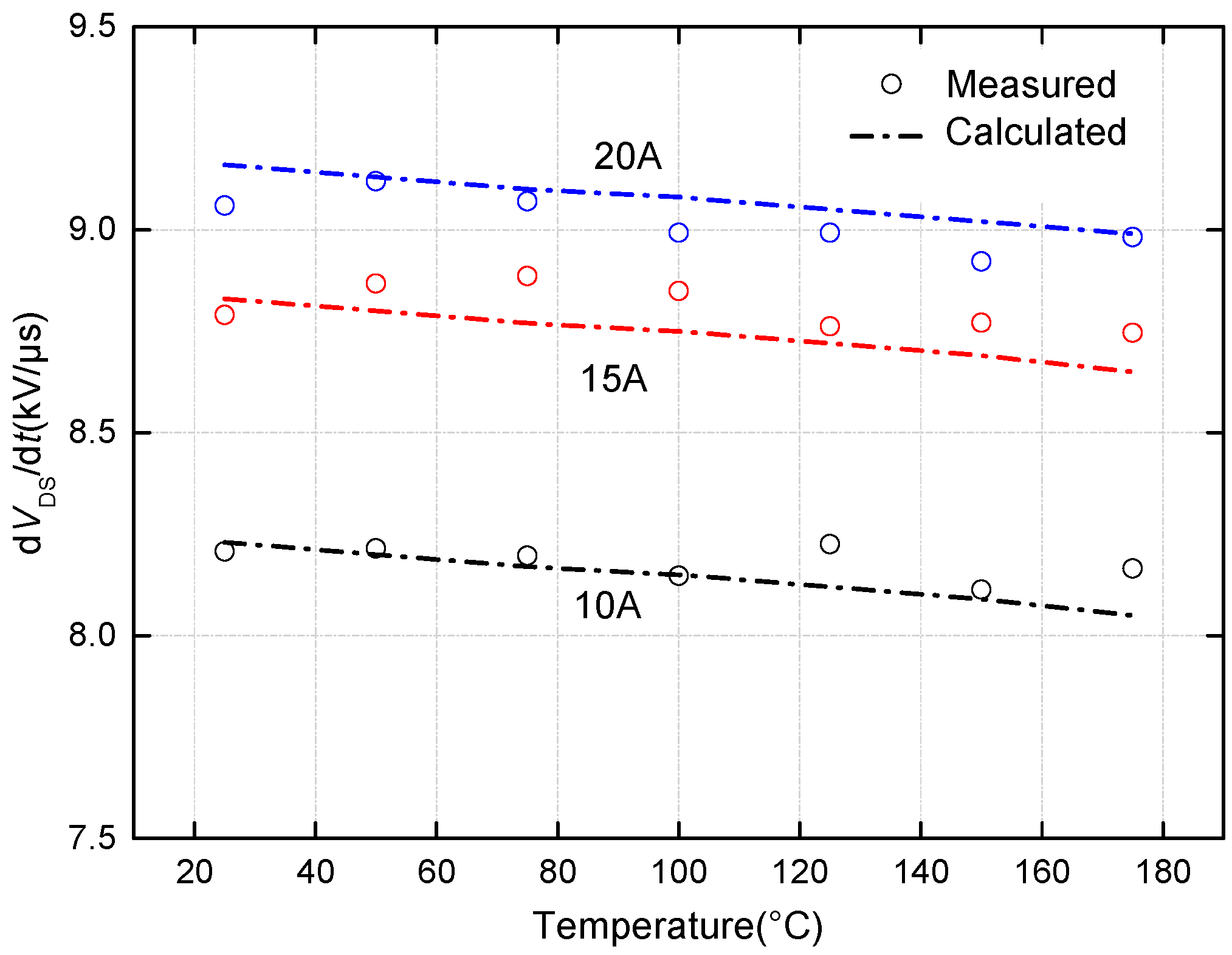
Figure 21.
Measured and calculated dVDS/dt as a function of temperature at a load current of 15 A and a gate resistor of 10 Ω during turn-off, shown for different voltages.
Figure 21.
Measured and calculated dVDS/dt as a function of temperature at a load current of 15 A and a gate resistor of 10 Ω during turn-off, shown for different voltages.

Figure 22.
Measured dVDS/dt as a function of temperature at a voltage of 400 V and a load current 15 A during turn-off, shown for different gate resistances.
Figure 22.
Measured dVDS/dt as a function of temperature at a voltage of 400 V and a load current 15 A during turn-off, shown for different gate resistances.

Figure 23.
Measured and calculated dVDS/dt as a function of temperature at a voltage of 400 V and a gate resistor of 10 Ω during turn-on, shown for different load currents.
Figure 23.
Measured and calculated dVDS/dt as a function of temperature at a voltage of 400 V and a gate resistor of 10 Ω during turn-on, shown for different load currents.
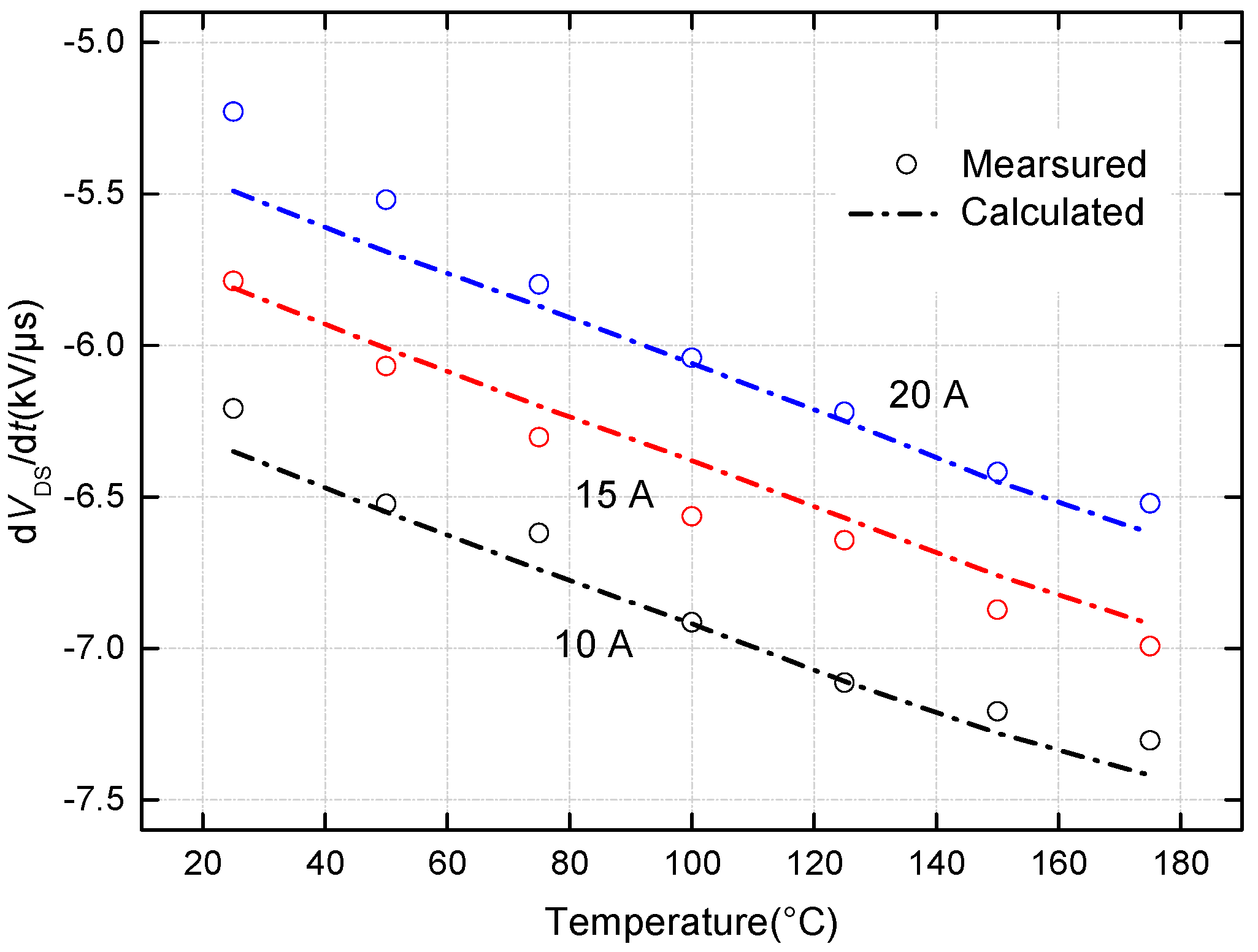
Figure 24.
Measured and calculated dVDS/dt as a function of temperature at a voltage of 15 A and a gate resistor of 10 Ω during turn-on, shown for different voltages.
Figure 24.
Measured and calculated dVDS/dt as a function of temperature at a voltage of 15 A and a gate resistor of 10 Ω during turn-on, shown for different voltages.

Figure 25.
Measured and calculated dVDS/dt as a function of temperature at a voltage of 400 V and a load current 15 A during turn-on, shown for different gate resistances.
Figure 25.
Measured and calculated dVDS/dt as a function of temperature at a voltage of 400 V and a load current 15 A during turn-on, shown for different gate resistances.

© 2017 by the authors. Licensee MDPI, Basel, Switzerland. This article is an open access article distributed under the terms and conditions of the Creative Commons Attribution (CC BY) license (http://creativecommons.org/licenses/by/4.0/).
Share and Cite
MDPI and ACS Style
Li, H.; Liao, X.; Hu, Y.; Huang, Z.; Wang, K. Analysis of Voltage Variation in Silicon Carbide MOSFETs during Turn-On and Turn-Off. Energies 2017, 10, 1456. https://doi.org/10.3390/en10101456
AMA Style
Li H, Liao X, Hu Y, Huang Z, Wang K. Analysis of Voltage Variation in Silicon Carbide MOSFETs during Turn-On and Turn-Off. Energies. 2017; 10(10):1456. https://doi.org/10.3390/en10101456
Chicago/Turabian StyleLi, Hui, Xinglin Liao, Yaogang Hu, Zhangjian Huang, and Kun Wang. 2017. "Analysis of Voltage Variation in Silicon Carbide MOSFETs during Turn-On and Turn-Off" Energies 10, no. 10: 1456. https://doi.org/10.3390/en10101456
Note that from the first issue of 2016, this journal uses article numbers instead of page numbers. See further details here.