Article

Control of a Three-Phase to Single-Phase Back-to-Back Converter for Electrical Resistance Seam Welding Systems

by
Simon Kissling
1,
Elie Talon Louokdom
2,*,
Frédéric Biya-Motto
2,
Bernard Essimbi Zobo
2 and
Mauro Carpita
3
1
Development of Power Electronics Systems (DEPsys), Route du Verney 20B, 1070 Puidoux, Switzerland
2
Laboratory of Electronics, Department of Physics, Faculty of Science, University of Yaoundé I, P.O. Box 812, Yaoundé, Cameroon
3
Département des Technologies Industrielles (TIN°), Haute école spécialisée de Suisse occidentale (HES-SO), University of Applied Sciences of Western Switzerland, Route de Cheseaux 1, CH-1401 Yverdon-les-Bains, Switzerland
*
Author to whom correspondence should be addressed.
Energies 2017, 10(1), 133; https://doi.org/10.3390/en10010133
Submission received: 21 November 2016 / Revised: 4 January 2017 / Accepted: 12 January 2017 / Published: 21 January 2017

Abstract

:
DC link back-to-back converters are widely used in industrial applications. This interest comes from their power factor unity capability on the utility grid and to maintain regulated output parameters, thanks to the decoupling between the grid and the load side. In this paper, a 150 KVA prototype of DC link back-to-back converter for electrical resistance seam welding applications is described. The focus of the paper is on the control strategy developed to absorb constant power from the three-phase utility grid. The key idea is to allow the voltage on the DC bus to vary in order to avoid the propagation at the input side of the pulsed power required by the load. An estimation procedure of the load parameters is presented too. The effectiveness of this control scheme has been proved by simulations and tests.

Graphical Abstract

1. Introduction

Electrical resistance welding (ERW) systems are widely used in the metallurgical and automotive industry [1,2,3,4]. This interest for ERW systems comes from their capability to make high-speed welding with good heat concentration, without additional materials, solvents, and shielding gas. This leads to weld with high productivity, low cost, and less pollution. The basic principle of an ERW system is to weld two materials using the heat generated by the passage of an electric current through the resistance formed by the contact between two metal surfaces [2]. Resistance seam welding (RSEW) is a particular ERW process where copper electrodes are disc-shaped to allow continuous welding of materials, commonly round or rectangular steel tubing. The electrodes rotate as the material passes between them. This allows the electrodes to stay in constant contact with the material to make continuous welds. RSEW typically applies low voltages and high welding currents in the range of 100 A–100 kA [2]. The welding current is one of the most important parameters of the welding process, as the amount of heat produced is proportional to its square.
In RSEW systems, single-phase high AC welding current is preferred compared to DC current used in resistance spot welding systems due to better electrode life performance, longer welding process, and the simplicity of use of the converter [3]. To perform at the above current requirement for RSEW power supply, a suitable high power converter is needed to feed a step-up current load transformer. The typical power converter topologies make use of an indirect voltage source configuration, made of a three-phase front-end diode rectifier with a DC-link capacitor, or thyristors with an inductor and capacitor (LC) power decoupling filter, and a pulse width modulated (PWM) single-phase inverter in both cases. However, both diode and thyristor topologies have the drawback to absorb a highly distorted current from the utility grid, and, in the case of thyristors, to draw reactive power and to create commutation line notching problems. Improvements in electromagnetic compatibility (EMC) standards proposes to solve those problems [5]. Additional PFC (power factor correction) circuits can be added to solve this problem. However, the solution proposed in this paper is to make use of a front-end PWM voltage source rectifier. Although many studies in the literature have dealt with indirect AC–AC converters with PWM rectifiers, they mainly treat the case of three-phase to three-phase conversion where constant power is transferred between the input and output side or single-phase to single-phase conversion [6,7,8,9,10,11]. Given the current and the PFC requirements for RSEW welding systems, a three-phase boost rectifier has to be used back-to-back with a single-phase voltage source inverter. This results in a three-phase to single-phase back-to-back converter topology studied in this paper. The main drawback to be taken into account for this application is that load parameters can vary in a non-linear way during the welding process [12]. This paper aims to propose a control strategy acting on the DC link voltage to absorb constant power from a three-phase grid and to deliver regulated output current and frequency to the load even in case of large load variations.
The paper is organized as follows: Section 2 presents the system topology and its mathematical description. Section 3 shows the proposed control strategy and simulations results. Section 4 shows the experimental results, and conclusions are given in Section 5.

2. System Description and Analysis

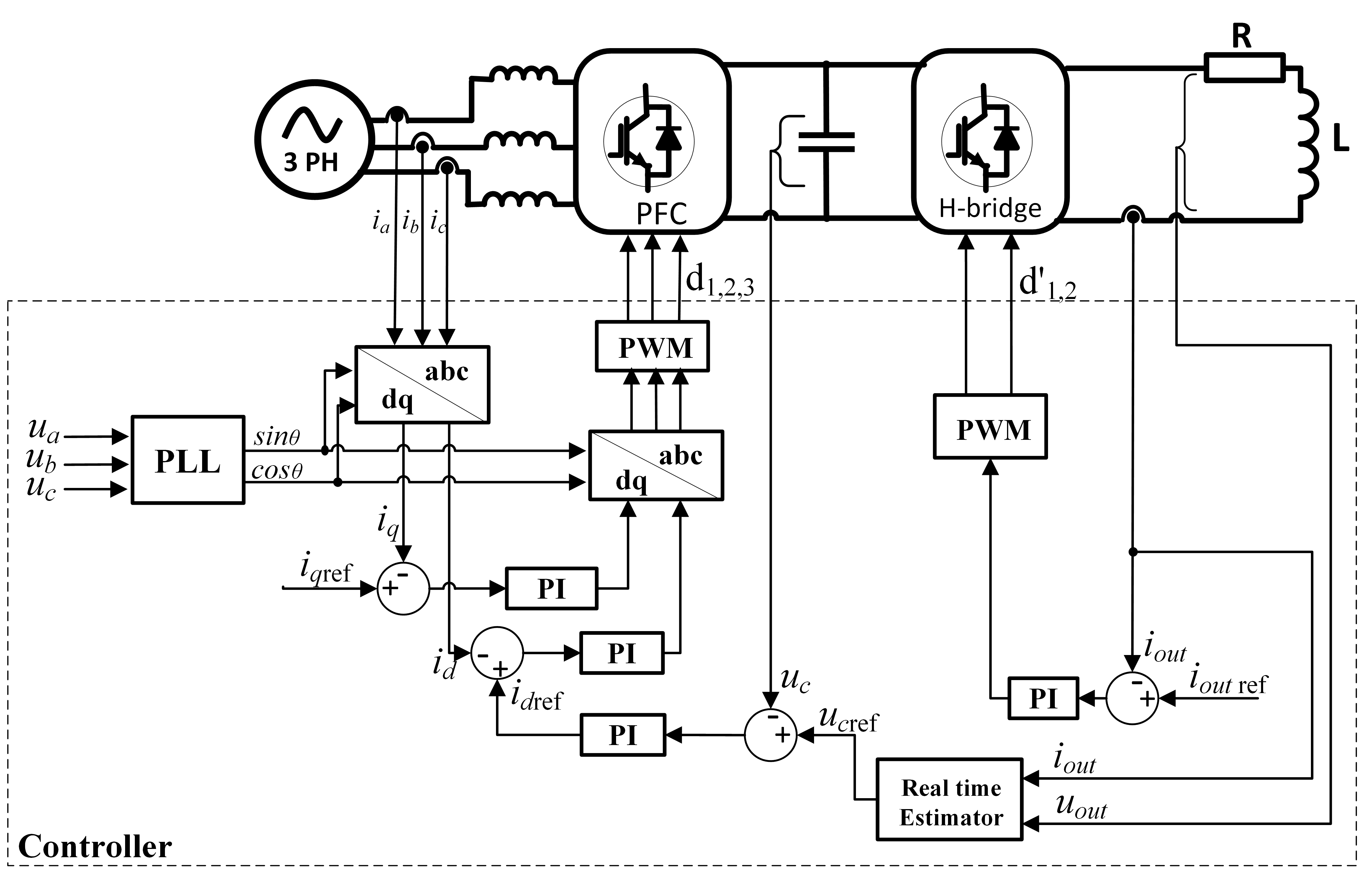
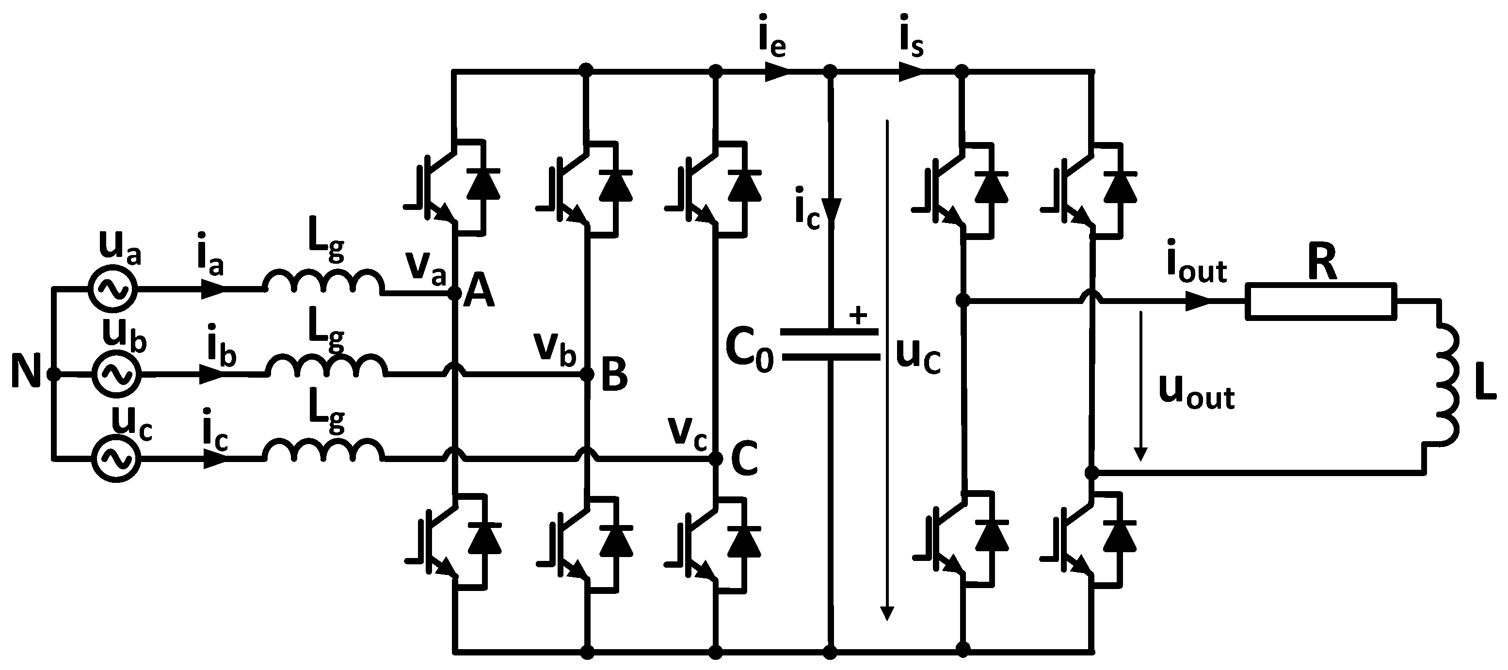
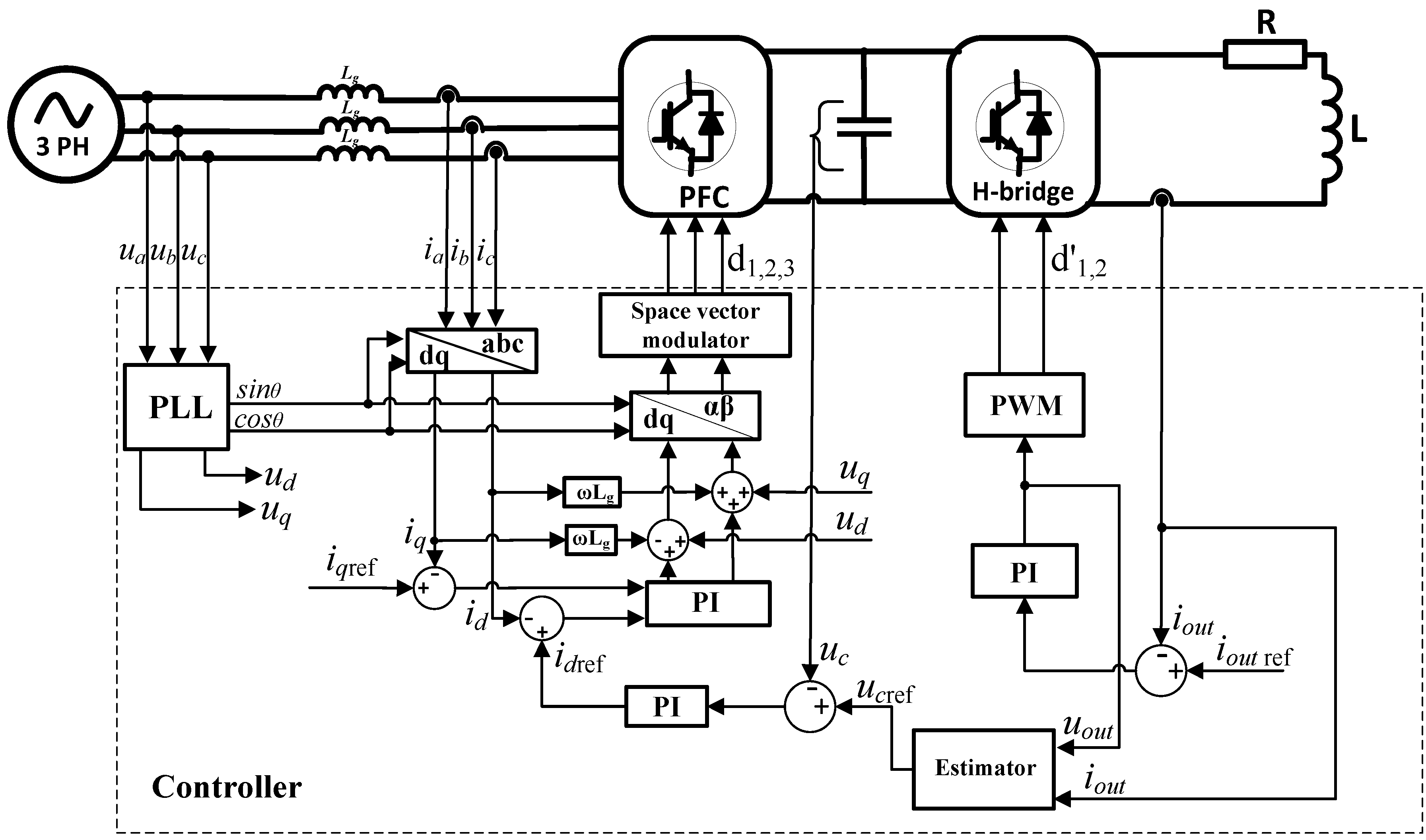
2.1. System Description

The converter schematic is shown in Figure 1. On the grid side there is a three-phase voltage source rectifier fed through coupling inductances. On the load side there is a single-phase, full bridge voltage source inverter. Both converters are controlled by PWM techniques. The DC link has been designed to allow a DC voltage variation between 650 V and 850 V, with a nominal value UCnom of 780 V. This choice allows for a variation range of the DC link large enough to guarantee the proper functioning of the boost voltage source rectifier [11]. For studying the system, the load has been modeled by an equivalent resistance and inductor (RL) circuit. This model is suitable to represent the short-circuited transformer used for the preliminary tests presented in Section 2 and Section 3. The behavior of the system with the real load will be presented in the Section 4.

2.2. Mathematical Description of the System

Since the goals in this paper are to control the power factor, to regulate the DC link capacitor voltage, as well as the output current, the equations derived in this section highlight the grid currents and the capacitor voltage.

2.2.1. Pulse Width Modulated Rectifier

Let us consider a three-phase utility grid. Using Figure 1, the three-phase variables can be expressed in the synchronous rotating coordinates as:
u d = L g d i d d t ω g L g i q + v d u q = L g d i q d t + ω g L g i d + v q .
The real and reactive powers supplied from the source are given by:
p = 3 2 ( u d i d + u q i q ) q = 3 2 ( u d i q u q i d ) .
If the d-axis of the rotating reference frame is well aligned with the AC voltage vector so that uq = 0, the instantaneous real and reactive powers absorbed from the utility grid are given by:
p = 3 2 u d i d q = 3 2 u d i q .
If only real power is transferred from the grid to the DC link (iq = 0), the power balance relationship between the AC input and DC output is given as:
3 2 U ^ g i d = u C i e .

2.2.2. Power Pulsation Compensation

In order to perform an effective power pulsation compensation, a power decoupling capacitor voltage command has to be established to compensate for power pulsation on the load side. Let us consider the system in a sinusoidal steady-state. The current and voltage on the output side can be expressed as:
i o u t ( t ) = I o u t 2 sin ( ω o u t t ) u o u t ( t ) = U o u t 2 sin ( ω o u t t + φ o u t ) ,
where Uout and Iout are the effective values of the output voltage and current, ωout is the output angular frequency, and φ o u t is the phase displacement between the two. The instantaneous power pout (t) on the load is given by:
p o u t ( t ) = u o u t ( t ) i o u t ( t ) = U o u t I o u t cos ( φ o u t ) [ 1 cos ( 2 ω o u t t ) ] + U o u t I o u t sin ( φ o u t ) sin ( 2 ω o u t t ) ,
and the instantaneous active power pactive_inst (t) on the load is:
p a c t i v e _ i n s t ( t ) = U o u t I o u t cos ( φ o u t ) [ 1 cos ( 2 ω o u t t ) ] .
The instantaneous active power varies at two times the output current frequency. If the PFC rectifier is forced to absorb a constant power from the utility, the voltage variation on the DC link will follow the frequency of the instantaneous active power. As a matter of fact, assuming that the constant power supplied by the utility is equal to the active power Pactive of the load, neglecting the losses on the rectifier and inverter, we have:
P g r i d = P a c t i v e = U o u t I o u t cos ( φ o u t ) .
From the power balance between the input and output, the power on the DC link capacitors can be expressed as:
p c a p ( t ) = P a c t i v e p o u t ( t ) = U o u t I o u t cos ( 2 ω o u t t + φ o u t ) = u C ( t ) C 0 d u C ( t ) d t .
The voltage of the capacitor tank can be obtained by integrating Equation (9):
u C 2 ( t ) = U o u t I o u t sin ( 2 ω o u t t + φ o u t ) C 0 ω o u t + c s t
where cst is an integration constant. Supposing that when t = 0, the voltage across the capacitor tank has its nominal value UCnom, we can rewrite Equation (10) as:
u c ( t ) = U C n o m 2 + U o u t I o u t C 0 ω o u t sin ( 2 ω o u t t + φ o u t ) U o u t I o u t C 0 ω o u t sin ( φ o u t )
Equation (11) highlights the variation of the DC link voltage due to the single-phase load. Some studies have addressed this DC link voltage ripple issue by adding a buffer circuit into the DC link to decouple the power ripples [13], or by using a ripple port module for ripple cancellation purposes [14]. However, using such solutions in our case will increase the number of components, the complexity, and the cost of the system. Moreover, given that, in our application, the output current frequency is allowed to vary within a range depending of the material to weld, many buffer circuits corresponding to each possible frequency of the output current would be necessary. In [15], it has been proposed to mitigate the propagation of the power fluctuation of a variable speed wind turbines on the utility side by allowing the DC link voltage to vary within a certain range. Such an approach will be used in this paper to compensate the power pulsation due to the single phase load. For that, Equation (11) provides a suitable DC link reference voltage to use.

3. Control Strategy

3.1. Unity Power Factor Formulation

Power quality is performed when the total harmonic distortion (THD) generated by the converter at the point of common coupling is less than 5% with a power factor (PF) greater than 0.99 [16]. The power factor calculation can be performed using Equation (12), where φ represents the phase displacement between the fundamental of the current and voltage:
PF = cos ( φ ) 1 + THD 2
If the load parameters of the converter are constant and well-known, the PF requirement can be simply achieved by providing the appropriate current reference to the PFC rectifier. The most commonly used control strategy for PFC rectifier is the voltage-oriented control (VOC) [11]. It is based on an external DC voltage control loop and an internal current decoupled control loop. The inner closed-loop current control is done in a rotating reference frame. The three-phase measured values are converted to an equivalent two-phase stationary system αβ and are then transformed to the rotating coordinate system dq using Clark and Park transformations. Proportional and integral (PI) regulators are used on DC values id and iq presented in Equation (1), to eliminate steady-state error. A unity power factor is obtained by forcing the current reference value iqref to be zero, while idref is set to control the active power flow. The output signals from the PI controllers after dq to αβ transformation are used for switching signal generation by a space vector modulator (SVM). A SVM is chosen to generate the PMW rectifier command because it allows to extend the linear domain of about 15%. In the case of the converter studied here, unit power factor can be achieved by using the same approach and by setting the DC link voltage reference to follow Equation (11).

3.2. Control of the Output Current

The control of the output current is performed using a classical current loop. This output control loop is decoupled from the rectifier control loop due to the capacitor tank. The current flowing through the load inductor is measured and compared to its reference value. A PI controller uses the error signal to provide the voltage command which will be compared to the inverter carrier signal in order to generate the PWM commands for the inverter switches.

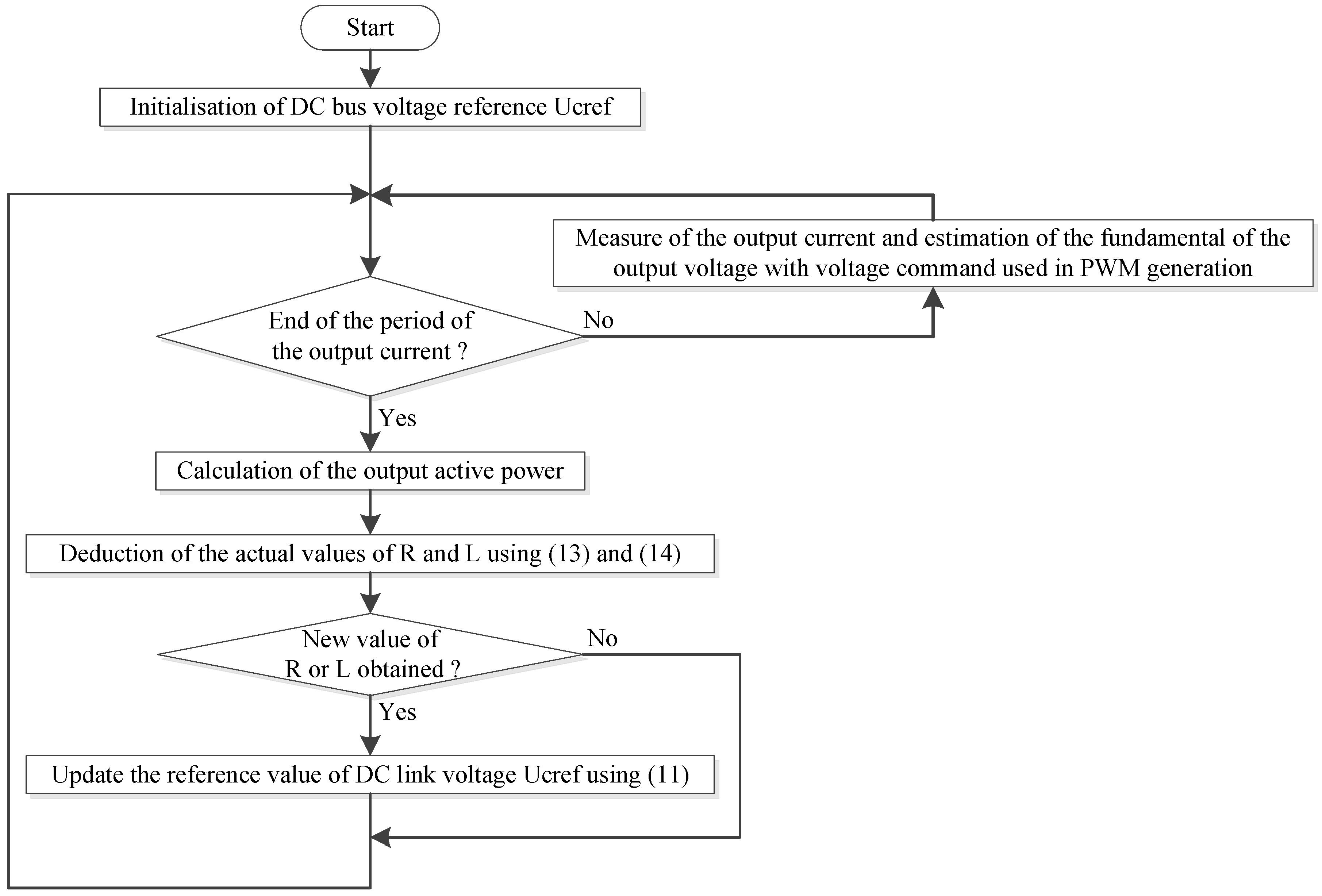
3.3. Proposed Estimation of Equivalent Load Parameter’s Values

When load parameters vary, the reference current id varies around its average value and the amplitude of the ripple is related to the gap between the preset values of the load parameters and their real values. The ripple of the reference current id around its average value leads to a variable power absorption on the utility grid and increases the harmonic distortions of the grid current. Then, the control strategy has to be adapted to cope with those variations.
The relationship between the voltage across the capacitors and the phase displacement on the output side is known from Equation (11). Given that the phase displacement is directly related to the resistance and inductance of the load, it is possible to handle their variations by providing the appropriate DC bus voltage reference to the PFC rectifier. This requires a suitable estimation of the equivalent load parameters.
As previously mentioned, the load is modelled by the series connection of a resistance and an inductance. The value of these two parameters must be estimated. In order to evaluate the value of the resistance, the active power absorbed by the load can be used. The single-phase inverter output current and voltage are measured. Active power Pactive is evaluated each period and the actual value of resistance can be obtained using Equation (13):
R = P a c t i v e I o u t 2
If the actual value of the resistance is known, the actual value of the inductance can be estimated using Ohm’s law, as in Equation (14):
L = U o u t 2 I o u t 2 R 2 ω o u t
The equivalent R, L estimation algorithm is shown in Figure 2. To optimize the digital signal processor (DSP) computational load, the proposed strategy will update the estimated parameters once each period. Given that the measures might be prone to noise, measurements are first filtered to reject any disturbances before being used in the estimation scheme.

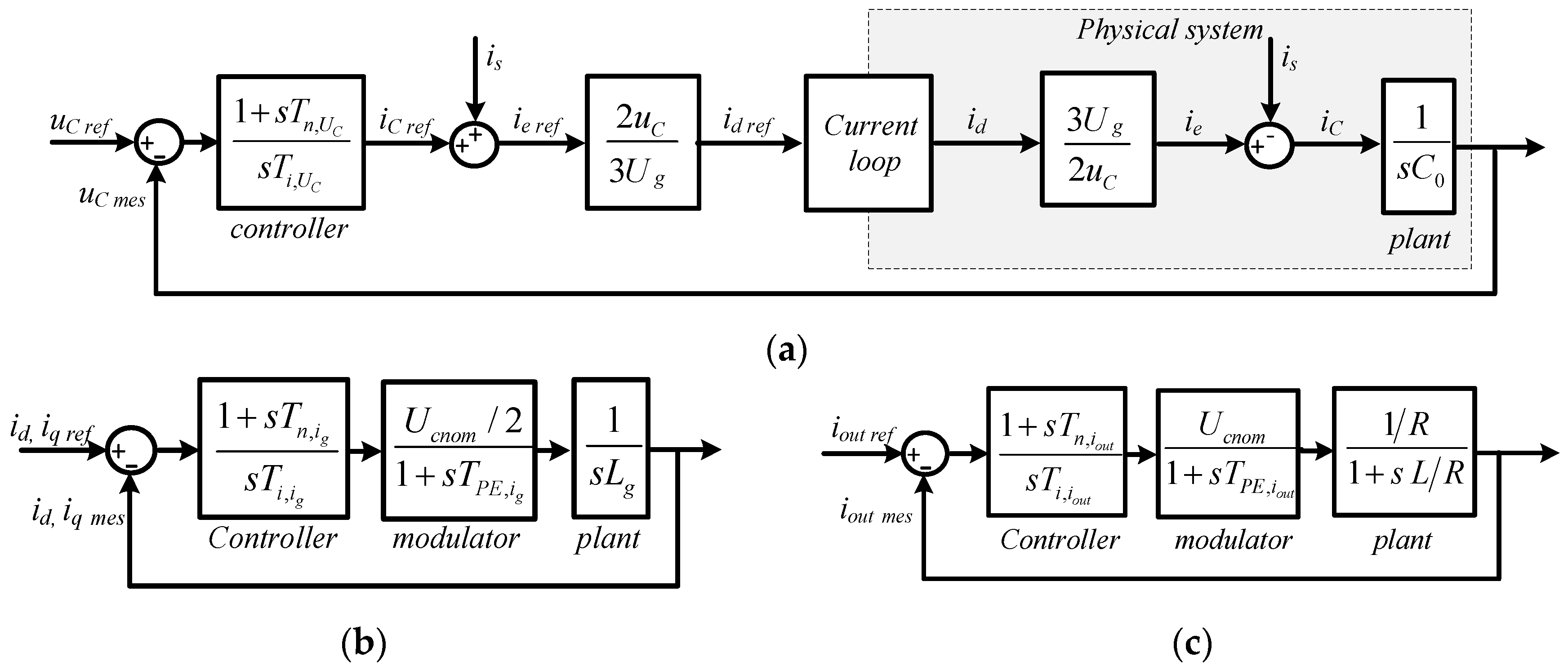
3.4. Tuning of the Controllers

In order to eliminate the steady—state error, PI controllers are used at all control stages. The PI controller transfer function is given in the Equation (15) where Tn and Ti are the time constants of the integral correlation and the integral action, respectively:
C ( s ) = 1 + s T n s T i
Using Equation (1), and taking into account the PWM modulator model, the current control loop can be equivalently represented by Figure 3b, where TPE represents the switching period and the sum of all of the parasitic process time constants. The DC link voltage is regulated using the active power carrying component of the grid current. Given Equation (4), the current flowing through the DC link capacitor can be expressed as:
i c = C 0 d u C ( t ) d t = 3 U ^ g i d 2 u C i s
Using Equation (16), the DC link voltage control loop can be equivalently represented by Figure 3a. By using the same approach, the output current control loop can be represented by Figure 3c. Once the control loops are obtained, the coefficients of the controller can be designed using modulus and symmetrical optimum, such as that presented in [17]. Table 1 summarizes the obtained controller parameters.

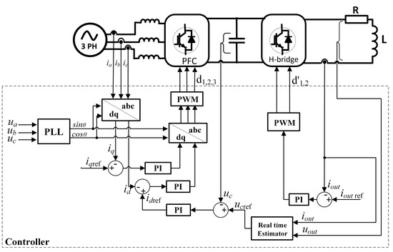
3.5. Overview of the Control System

The block diagram of the whole structure of the controller is presented in the Figure 4. A closed loop phase locked loop (PLL) module has been added for the synchronization to the grid, such as that in [18].

3.6. Simulations Results

Circuit parameters are presented in Table 2. Simulations are performed using PLECS© software [19]. The active rectifier is controlled in the rotating frame dq as mentioned in the previous sections. A unit power factor is then obtained by forcing the current reference value iqref to be zero, while idref is set to control the active power flow.

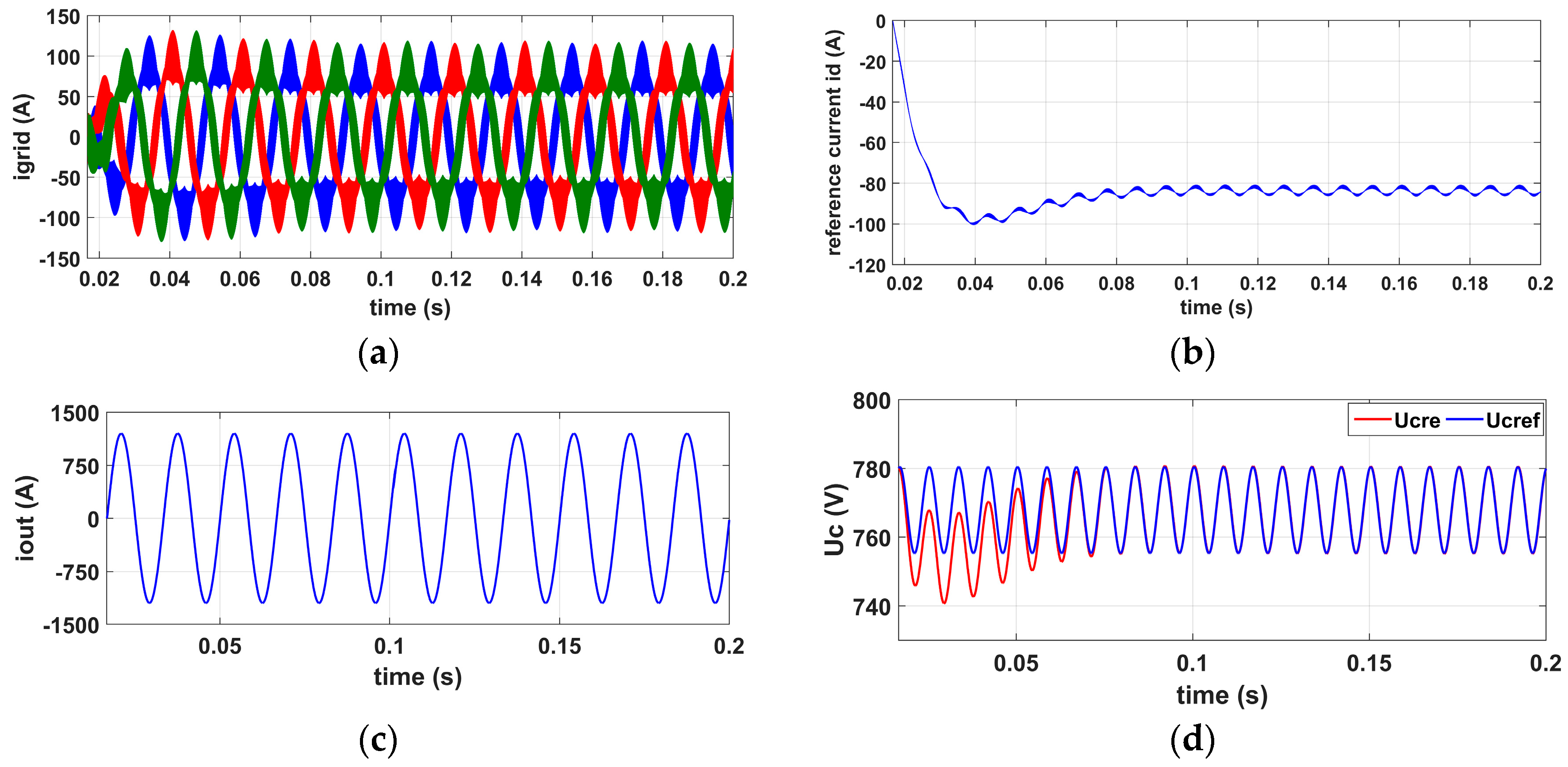
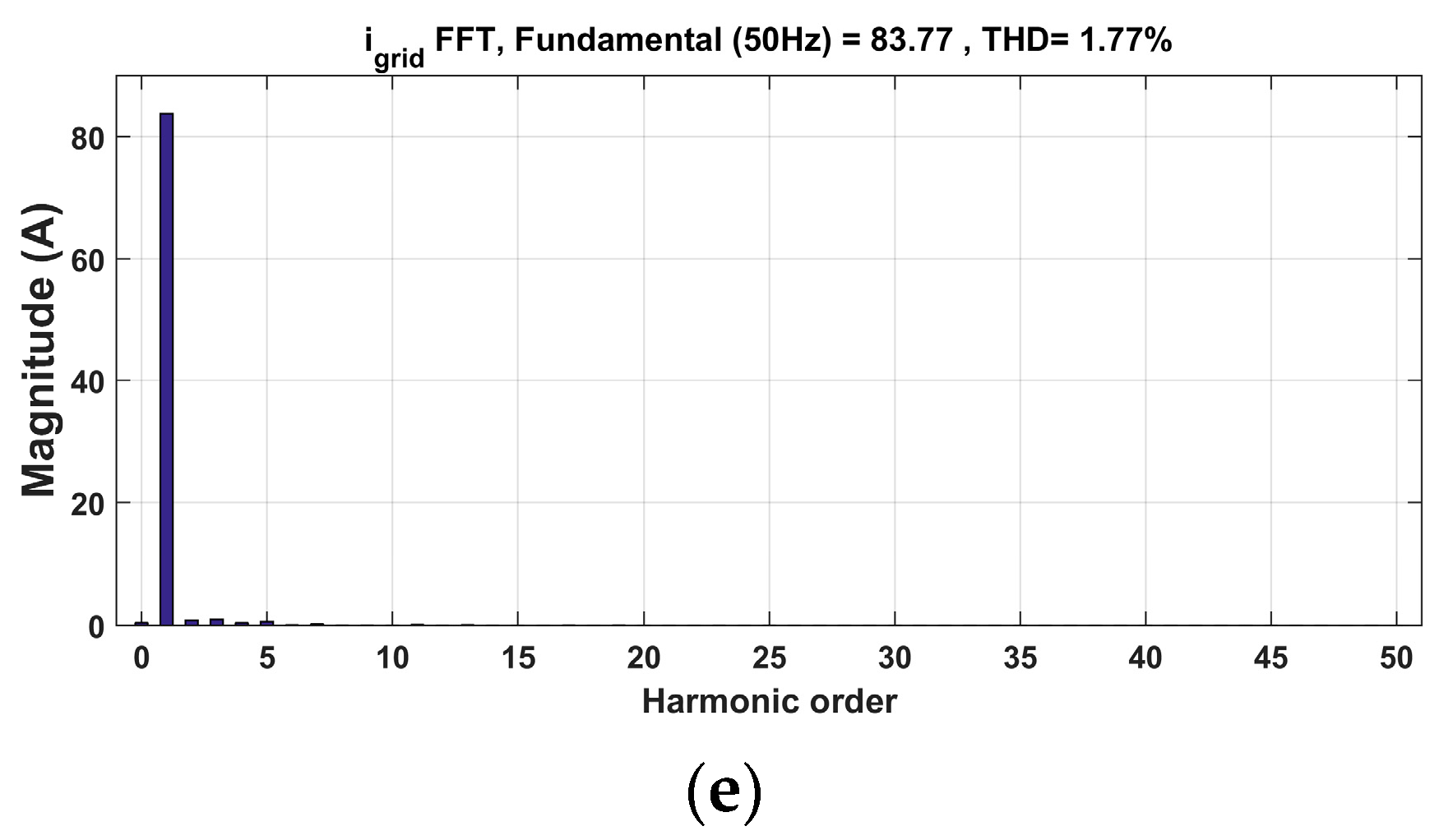
3.6.1. Constant Load Simulations

Figure 5 presents a simulation where the load parameters are constant. In this simulation, the PFC rectifier has been set to follow the theoretical DC voltage ripples expressed in Equation (11) (Figure 5d). One can see in this figure that the pulsed power on the load side does not affect the feeder side. A constant power is supplied by the grid because the variations on the reference current id shown in Figure 5b are very small (less than 3% between instants t = 0.16 s and t = 0.18 s) and the grid currents present regular amplitudes (Figure 5a). Output current is well regulated (Figure 5c) and the power factor calculated using Equation (12) is about 0.99 with a THD = 1.77% (Figure 5e).

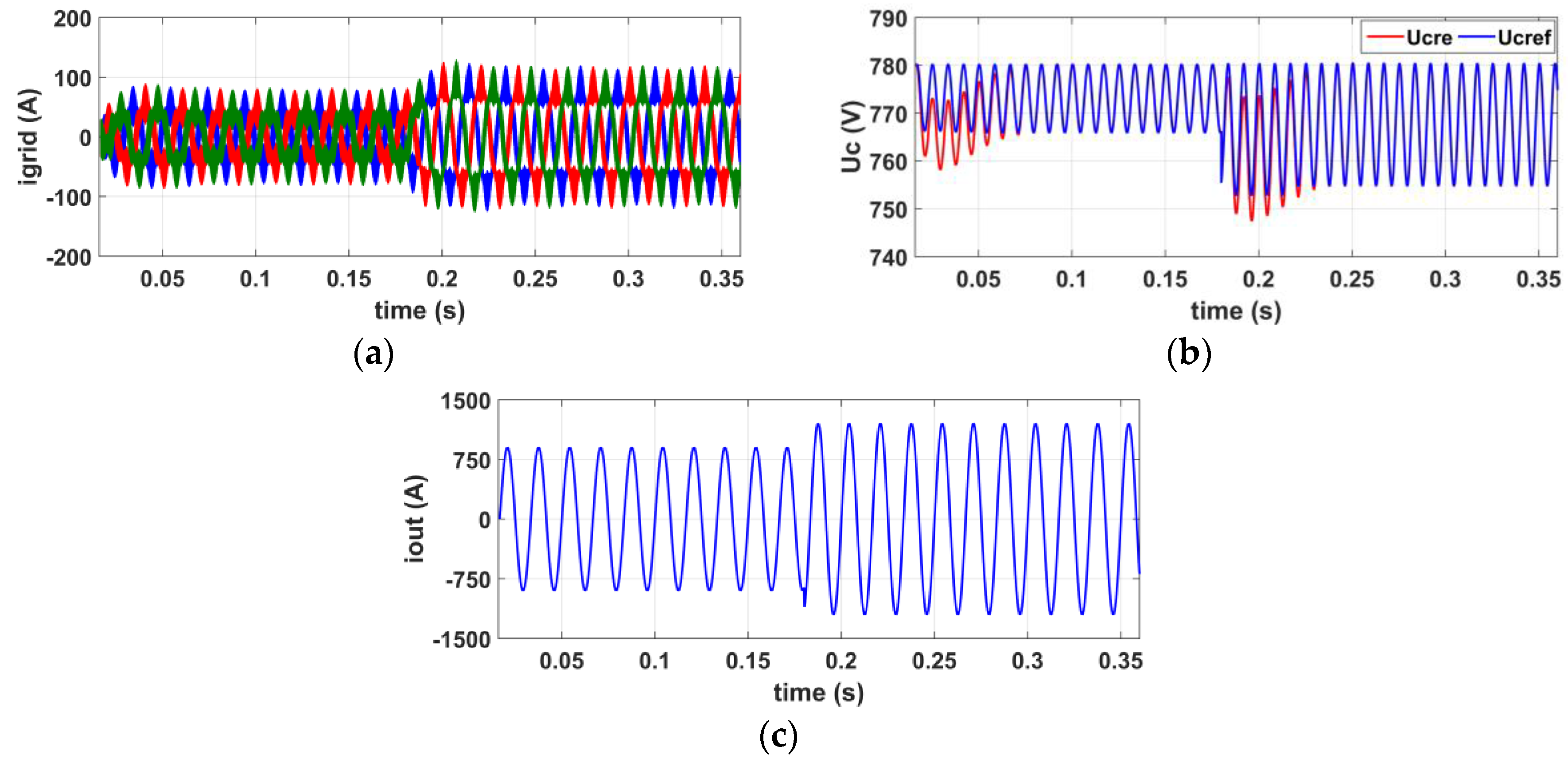
3.6.2. Step Change in the Output Current Reference

A second simulation shows the response of the controller with an output current reference step. Simulations results are presented in the Figure 6. At t = 0.18 s, the output current reference amplitude steps from 900 A to 1200 A. Good controller dynamics can be observed.

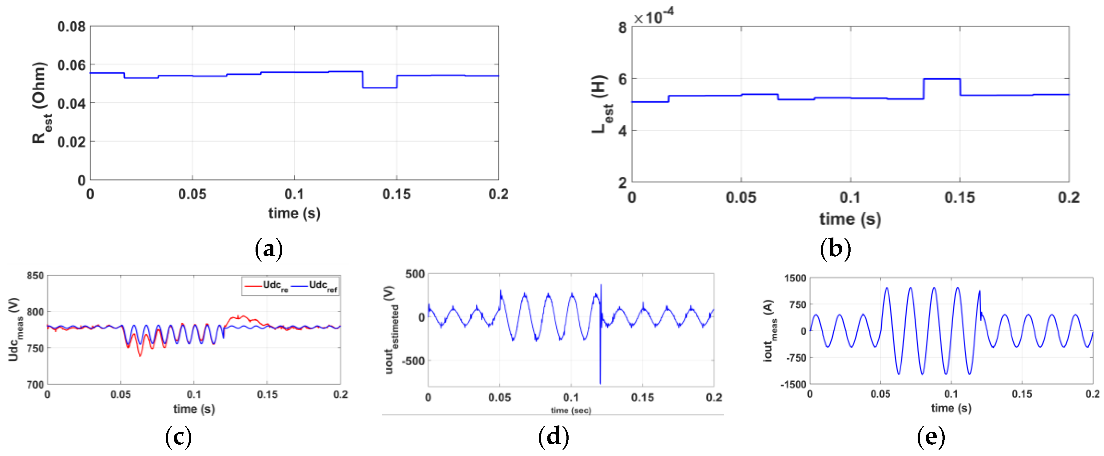
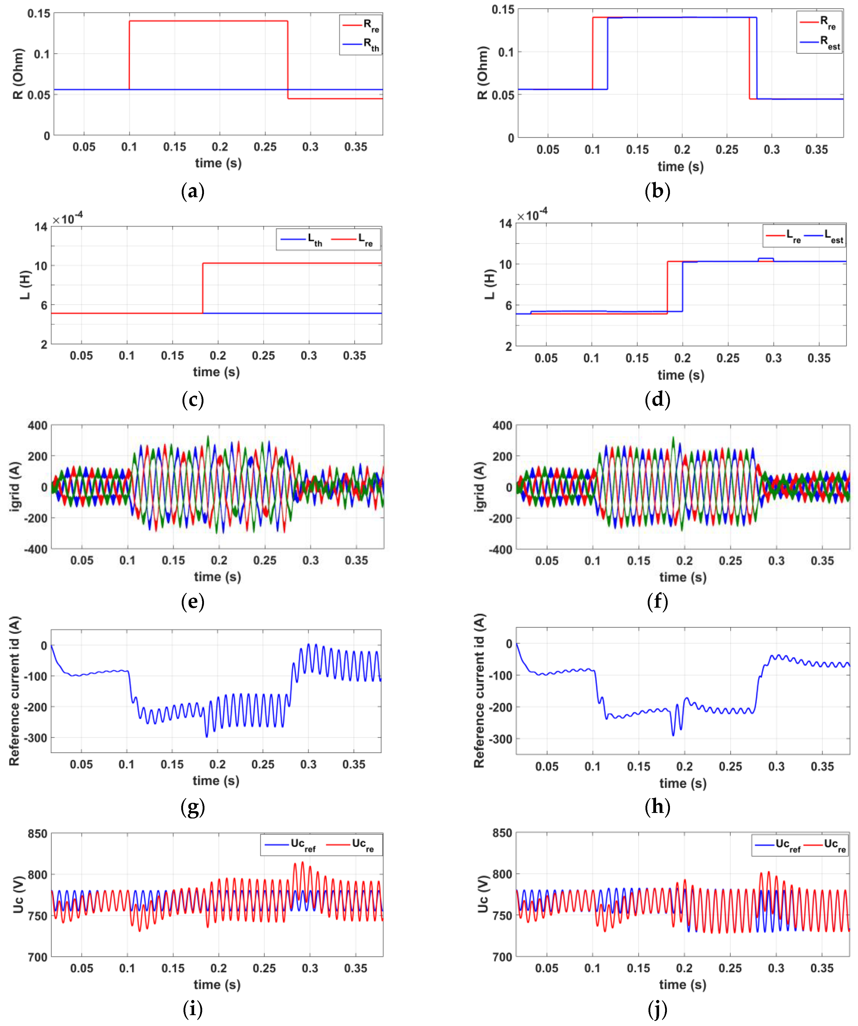
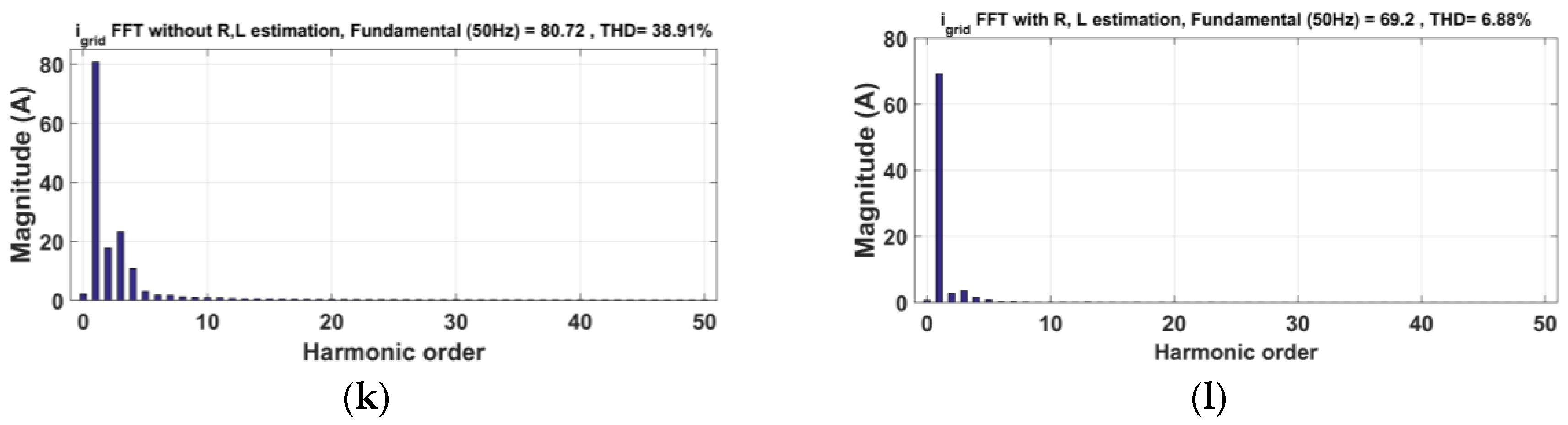
3.6.3. Step Change of Output Parameter Values

A third simulation shows the behavior of the controller with a step change of the load resistance and inductance. The left column of the Figure 7 presents the waveforms obtained without tracking the load parameter, while the right column of the Figure 7 shows the waveforms with the proposed control scheme, including an estimation of load variations. At the beginning of both simulations, the theoretical load resistance and inductance in the controller are equal to their actual circuit values. At t = 0.10 s, the load resistance is changed from R to 2.5R. At t = 0.183 s, the load inductance is changed from L to 2L, and at t = 0.275 s, the load resistance is changed from 2.5R to 0.8R. The actual and estimated resistance and inductance values are shown in Figure 7b,d, respectively. The estimation delay is, at most, one period of the output current. The choice to update the load parameters at the end of each period of the output current instead of making a sliding average is made to be as close as possible to the hardware implementation. In fact, the frequency of the output current can be set in a range of 5–80 Hz depending on the type of the material to weld. Making a sliding average at low frequency might cause an overflow of the microcontroller’s memory due to the sampling period. However, this update delay does not significantly affect the control scheme.
When the controller does not take into account the load variations (left column of Figure 7), grid currents present harmonic distortions and irregular amplitudes (Figure 7e,k), leading to fluctuating power supplied by the three phase grid. This results in a large ripple of the reference current id around its mean value (Figure 7g). For example, the id reference current’s ripples between instants t = 0.32 s and t = 0.36 s is about 51.4%, leading to a power factor of about 0.90 with a THD = 38.91%. On the other hand, when the load parameters are estimated and are included in the calculation of the DC bus voltage reference (Figure 7j compared to Figure 7i), their variations do not affect grid currents. This leads to regular amplitudes of the latter (Figure 7f) and, hence, constant power is drawn from the grid. The id reference current’s ripples around its mean value between instants t = 0.32 s and t = 0.36 s is now about 4.6%, corresponding to a reduction of about 91% and resulting to a power factor of about 0.99 with a THD = 6.88%. The THD has, thus, been reduced by about 82%. This confirms the effectiveness of the proposed adaptive scheme.

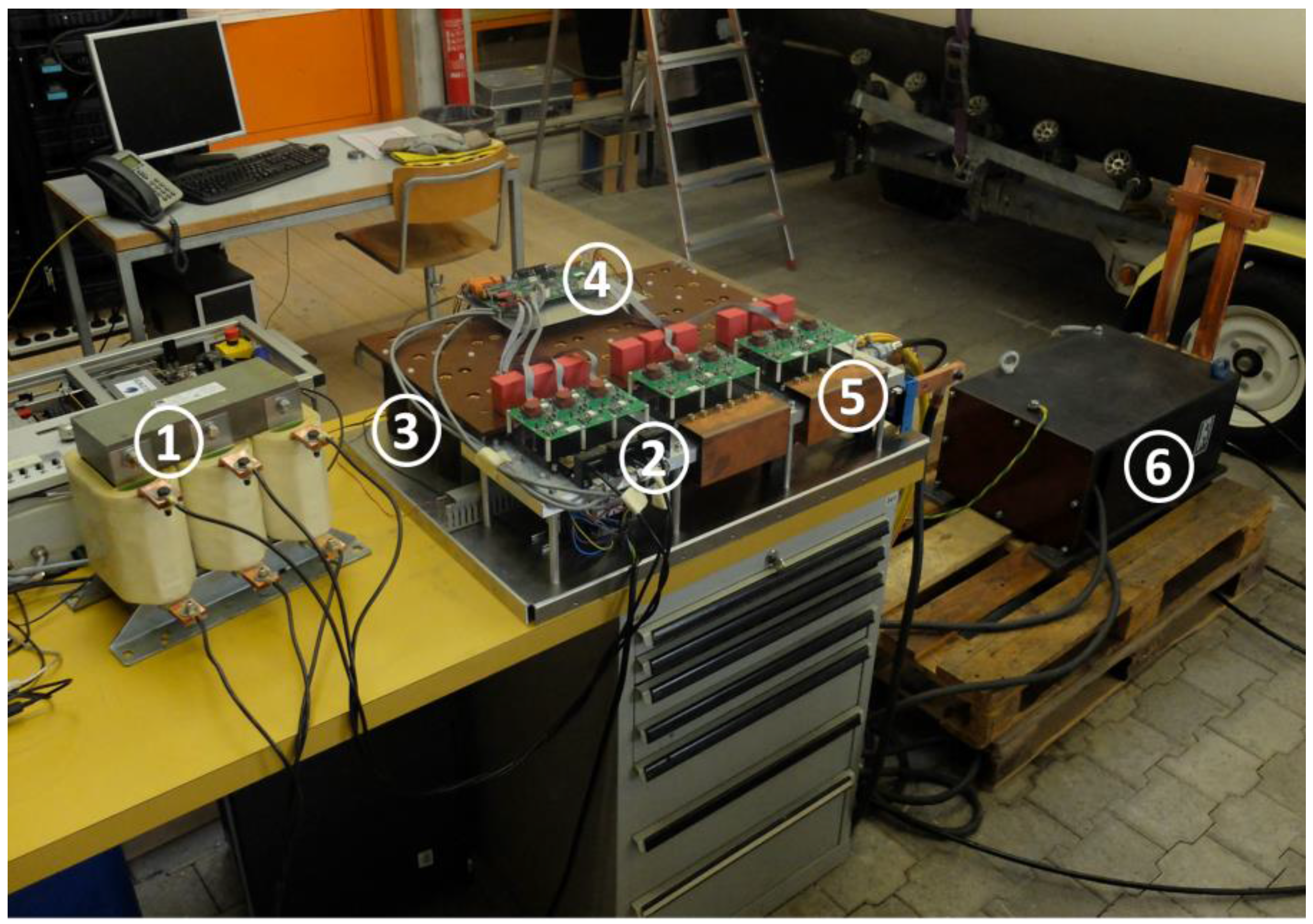
4. Experimental Results

In order to verify the expected behavior of the control scheme, a full-scale prototype has been built. The specifications of the experimental setup are the same as in Table 2. The layout of the prototype is shown in Figure 8. This prototype consists of a capacitor tank designed for a voltage up to 900 VDC, a three-phase rectifier and a full bridge inverter both using Fuji insulated gate bipolar transistor’s (IGBT) (6MBI450V-120-50) [20], a three-phase coupling inductance and a load. The control of the whole system shown in Figure 4 has been implemented on a single Texas Instruments TMS320F28335 “Delfino” microcontroller [21]. Two series of tests are presented in the following sections. The first set of tests has been done on a full scale dummy load and the second set of tests has been done on a resistance seam welding system.

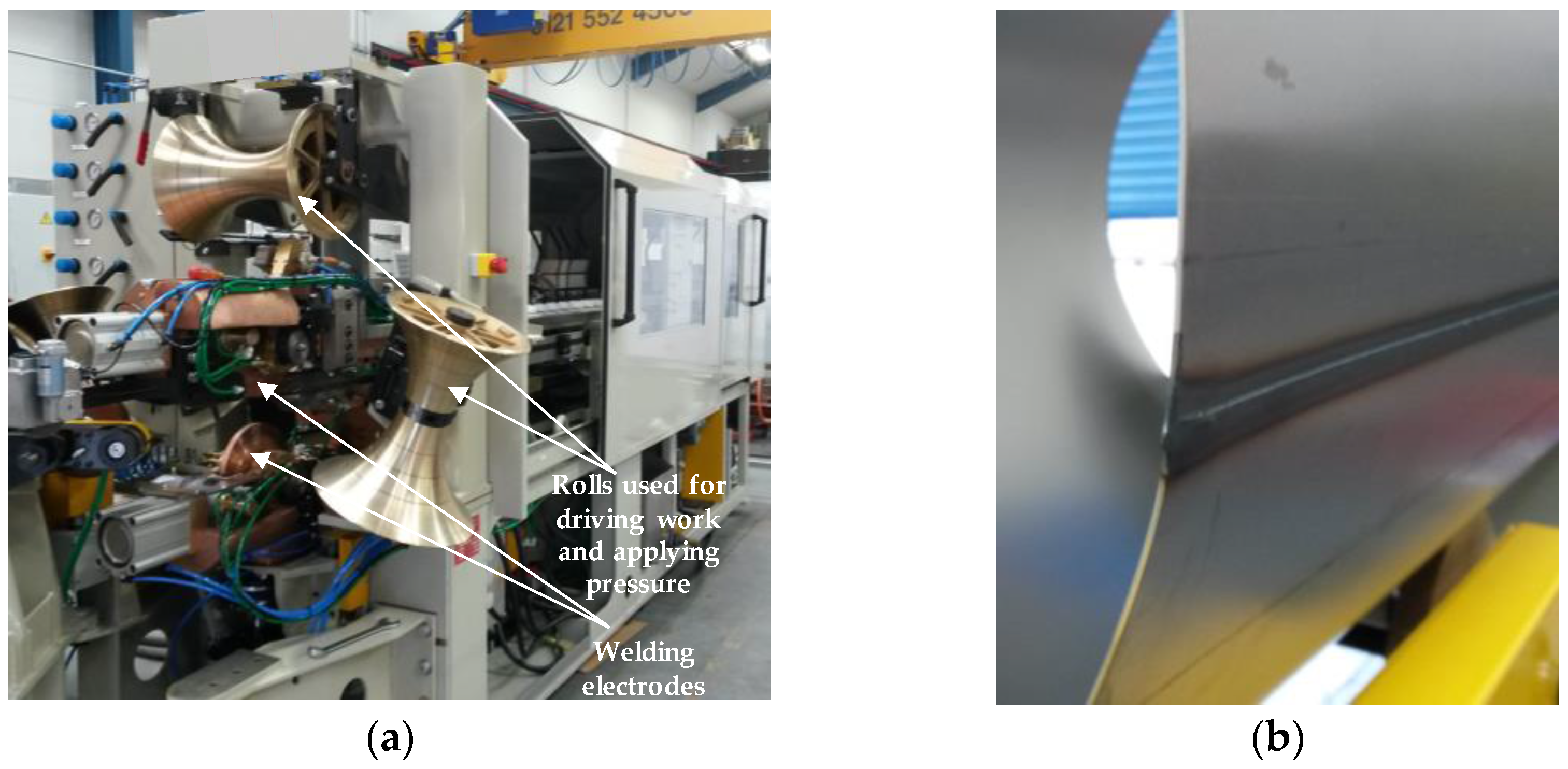
4.1. Tests on a Dummy Load

The dummy load used consists of a short-circuited high-power transformer with a 1:30 turn ratio. Figure 9a–c show the waveforms of a test performed at Iout = 848 A and Sout = 144 kVA. Two phases of the grid current and one phase of the grid voltage are presented in Figure 9a. The voltage (pink trace) and its corresponding current (blue trace) are perfectly synchronized. In this case, the power factor calculated using Equation (12) is about 0.99. Grid currents show regular amplitudes. Figure 9b shows the DC bus voltage for the same operating point as above. The ripple ratio of DC bus voltage is a little bit higher (2%) than the simulation results shown in Figure 5d. This is due to the losses on the inverter and to component tolerances. Figure 9c presents the harmonic spectrum of the grid current presented in Figure 9a (blue trace). One can denote a low harmonic content with a THD of about 9.69%. Figure 9d shows the output current at Iout = 106 A, Sout = 2.25 kVA.
Figure 10 presents waveforms plotted with samples recorded using the microcontroller to test the response of the controller with an output current reference step and the load parameter‘s estimation scheme. At t = 0.05 s, the amplitude of the output current reference steps from 450 A to 1200 A (exactly at the beginning of the output current period), and at t = 0.12 s the amplitude is changed from 1200 A to 450 A (generic instant within a period). Figure 10a,b present the load resistance and inductance estimations over time. A smooth transition occurs after the first step. A peak is observed on the output voltage (Figure 10d) after the second step. However, the controller effectively handles the instantaneous variations of the output current reference. Test results demonstrate the correct behavior of the proposed control strategy.

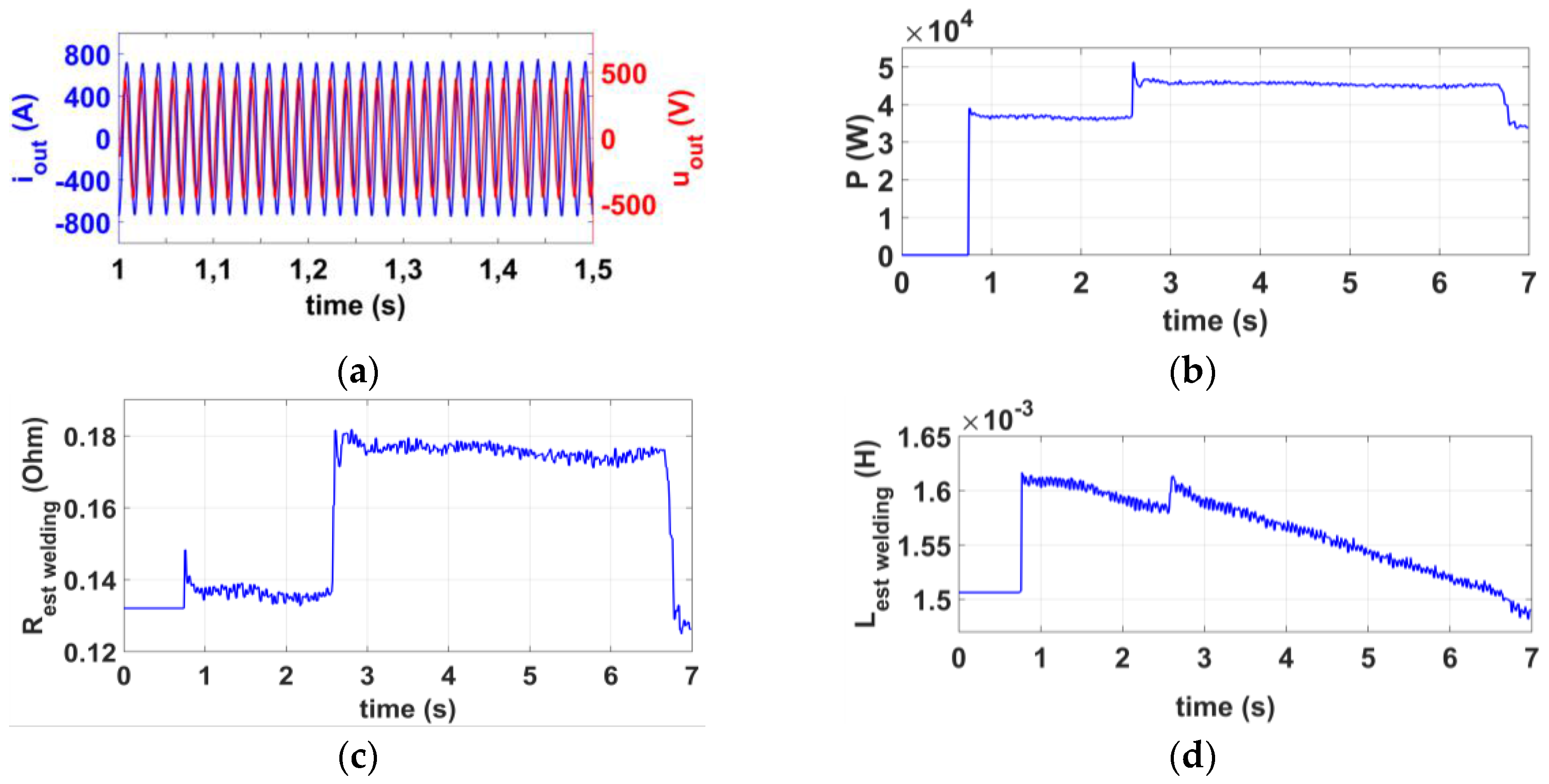
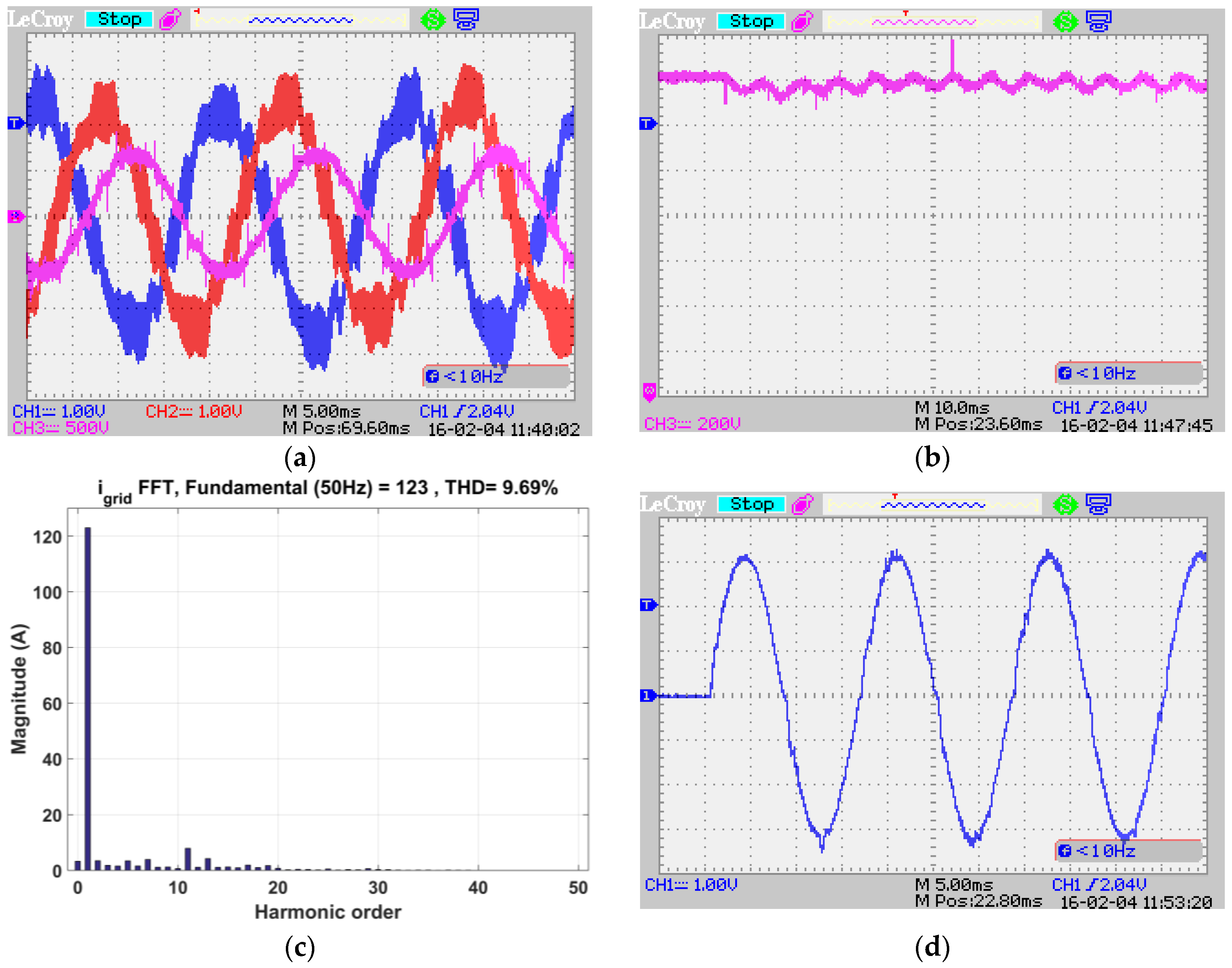
4.2. Welding Test with the Converter

The welding test has been performed on a functional RSEW system where its traditional power converter has been replaced by the prototype presented in Figure 8. The effective value of the output current required to perform a barrel weld was about 500 A. The whole welding system and the barrel welded when using the prototype as the power converter are presented at the Figure 11.
The whole welding process is carried out in approximately 7 s. Figure 12 presents the estimated parameter’s traces during the welding process. Figure 12a presents the fundamental of the output voltage and the output current traces during the welding process used for the output power estimation (a section between t = 1 s and t = 1.5 s). Figure 12b presents the estimated active power at the output of the converter, whereas Figure 12c,d present the estimated load resistance and inductance, respectively. From t = 0 s to t = 0.8 s, the system is in idle state. Output resistance and inductance preset values are about 0.132 Ω and 1.5 mH, respectively. From t = 0.8 s to t = 2.6 s, the converter enters into normal operation. The welding electrodes are joined, but without the barrel to weld. A current is flowing between the electrodes and a power of about 36 kW is delivered at the output of the converter. At t = 2.6 s, the barrel to weld begins to flow between the welding electrodes. The output power of the converter steps from 36 kW to 46.5 kW (Figure 12b) and, hence, a useful power of about 10 kW for the welding. The output resistance is estimated over time, in steps from 0.13 Ω to 0.18 Ω (Figure 12c) and the estimated output inductance, which was decreasing, steps from 1.58 mH to 1.61 mH (Figure 12d). One can observe that the output parameters vary when the welding starts and during the welding process. This justifies a suitable estimation of those parameters over time and their integration into the control scheme.

5. Conclusions

This paper explores the control of a three-phase to single-phase back-to-back converter to achieve both a unit power factor and constant power on the utility grid and output regulated parameters for electrical resistance welding applications. The proposed control strategy is to vary the DC link voltage to manage the variations generated by the load, avoiding their propagation on the feeder side. A suitable estimation of the load parameters is also performed to handle the case of load variations. Simulation results proved that by allowing the DC link voltage to vary in a suitable manner, the requirement in terms of power factor can be achieved at the point of common coupling. Moreover, these simulation results have shown that taking into account the load variations in the control scheme can reduce the THD of grid currents by more than 80%. Tests have been carried out on a dummy load and on a real resistance seam welding machine. Both tests have confirmed good functioning of the estimation scheme and, hence, the effectiveness of the proposed control strategy.

Author Contributions

Simon Kissling initiated the study, designed the system and carried out experimental tests. Elie Talon Louokdom, Frédéric Biya-Motto and Bernard Essimbi Zobo performed the mathematical analysis of the converter and developed the simulation model. Elie Talon Louokdom analyzed the simulations and test results data. Mauro Carpita coordinated all the project’s activities starting from the design of the system to the experimental tests and the paper writing. All the authors equally contributed to the paper writing.

Conflicts of Interest

The authors declare no conflict of interest.

References

  1. Zhang, H.; Senkara, J. Welding metallurgy. In Resistance Welding Fundamentals and Applications; Taylor & Francis Group: Boca Raton, FL, USA, 2006; pp. 1–16. [Google Scholar]
  2. Weman, K. Pressure welding methods. In Welding Process Handbook; Woodhead Publishing Limited: Cambridge, UK, 2003; pp. 87–91. [Google Scholar]
  3. Mathers, G. Resistance welding processes. In The Welding of Aluminium and Its Alloys; Woodhead Publishing Limited: Cambridge, UK, 2002; pp. 166–180. [Google Scholar]
  4. Winkler, T.; Doebbelin, R.; Lindemann, A. Mitigation of conducted emission of power electronic resistance welding equipment. In Proceedings of the Power Electronics and Motion Control Conference (EPE‑PEMC), Portoroz, Slovenia, 30 August–1 September 2006; pp. 450–455.
  5. International Electrotechnical Commission. Resistance Welding Equipment. Electromagnetic Compatibility (EMC) Requirements; IEC 62135-2; International Electrotechnical Commission: Geneva, Switzerland, 2015. [Google Scholar]
  6. Malesani, L.; Rossetto, L.; Tenti, P.; Tomasin, P. AC/DC/AC PWM converter with reduced energy storage in the DC link. IEEE Trans. Ind. Appl. 1995, 31, 287–292. [Google Scholar] [CrossRef]
  7. Dos Santos, E.C.; Da Silva, E.R. Advanced Power Electronics Converters: PWM Converters Processing AC Voltages; Wiley-IEEE Press: New York, NY, USA, 2014. [Google Scholar]
  8. Hwang, J.G.; Winkelnkemper, M.; Lehn, P.W. Control of AC-DC-AC converters with minimized DC link capacitance under grid distortion. In Proceedings of the IEEE International Symposium on Industrial Electronics, Montreal, QC, Canada, 9–13 July 2006; pp. 1217–1222.
  9. Friedli, T.; Kolar, J.W.; Rodriguez, J.; Wheeler, P.W. Comparative evaluation of three-phase AC–AC matrix converter and voltage DC-Link back-to-back converter systems. IEEE Trans. Ind. Electron. 2012, 59, 4487–4510. [Google Scholar] [CrossRef]
  10. Shen, L.; Bozhko, S.; Asher, G.; Patel, C.; Wheeler, P. Active DC-link capacitor harmonic current reduction in two-level back-to-back converter. IEEE Trans. Power Electron. Electron. 2016, 31, 6947–6954. [Google Scholar] [CrossRef]
  11. Kazmierkowski, M.P.; Krishnan, R.; Blaabjerg, F. Control of three-phase PWM rectifiers. In Control in Power Electronics: Selected Problems; Academic Press: San Diego, CA, USA, 2002; pp. 419–459. [Google Scholar]
  12. Salem, M. Control and Power Supply for Resistance Spot Welding (RSW). Ph.D. Thesis, Western Ontario University, London, ON, Canada, 2011. [Google Scholar]
  13. Ohnuma, Y.; Itoh, J. A control method for a single-to-three-phase power converter with an active buffer and a charge circuit. In Proceedings of the 2010 IEEE Energy Conversion Congress and Exposition, Atlanta, GA, USA, 12–16 September 2010; pp. 1801–1807.
  14. Harb, S.; Mirjafari, M.; Balog, R.S. Ripple-port module-integrated inverter for grid-connected PV applications. IEEE Trans. Ind. Appl. 2013, 49, 2692–2698. [Google Scholar] [CrossRef]
  15. Hu, W.; Chen, Z.; Wang, Y.; Wang, Z. Flicker mitigation by active power control of variable-speed wind turbines with full-scale back-to-back power converters. IEEE Trans. Energy Convers. 2009, 24, 24–640. [Google Scholar]
  16. Kolar, J.W.; Friedli, T. The essence of three-phase PFC rectifier systems—Part I. IEEE Trans. Power Electron. 2013, 28, 176–198. [Google Scholar] [CrossRef]
  17. Åström, K.J.; Hägglund, T. Controller design. In PID Controllers: Theory, Design, and Tuning, 2nd ed.; Instrument Society of America: Research Triangle Park, NC, USA, 1995; pp. 120–197. [Google Scholar]
  18. Kaura, V.; Blasko, V. Operation of a phase locked loop system under distorted utility conditions. IEEE Trans. Ind. Appl. 1997, 33, 58–63. [Google Scholar] [CrossRef]
  19. Electrical Engineering Software PLEXIM. Available online: http://www.plexim.com (assessed on 20 November 2016).
  20. IGBT Modules—6MBI450V-120-50. Available online: http://www.fujielectric-europe.com/downloads/6MBI450V-120-50_1734379.PDF (assessed on 20 November 2016).
  21. TMS320F28335 Delfino Microcontroller. Available online: http://www.ti.com/product/TMS320F28335 (assessed on 20 November 2016).
Figure 1. Three-phase to single-phase converter schematic, with the resistance and inductor (RL) equivalent load.
Energies 10 00133 g001
Figure 2. Flowchart of the R, L estimation algorithm.
Energies 10 00133 g002
Figure 3. Equivalent representation of the control loops. (a) DC link voltage control loop; (b) the grid current control loop; and (c) the output current control loop.
Energies 10 00133 g003
Figure 4. Structure of the controller. Proportional and integral (PI) denotes proportional and integral controller.
Energies 10 00133 g004
Figure 5. Waveforms on the converter with constant load where output power Sout = 140 KVA. (a) Grid currents; (b) reference current id in the dq frame; (c) output current iout; (d) DC bus voltage. UCre = real value (red trace), UCref = reference value (blue trace); and (e) the harmonic spectrum of one of the grid currents.
Energies 10 00133 g005aEnergies 10 00133 g005b
Figure 6. Waveforms on the circuit with change in the reference of the output current. (a) Grid currents; (b) DC bus voltage. UCref = reference value (blue trace), UCre = real value (red trace); (c) The output current iout.
Energies 10 00133 g006
Figure 7. Simulations results of a step change of load parameters. (a) Real and theoretical load resistance; (b) real and estimated load resistance; (c) real and theoretical load inductance; (d) real and estimated load inductance; (e) grid currents without estimation scheme; (f) grid currents with estimation scheme; (g) reference current id without estimation scheme; (h) reference current id with estimation scheme; (i) DC bus voltage reference and real DC bus voltage without the estimation scheme; (j) DC bus voltage reference and real DC bus voltage with the estimation scheme; (k) harmonic spectrum of one of the grid currents without the estimation scheme; and (l) harmonic spectrum of one of the grid currents with estimation scheme.
Energies 10 00133 g007aEnergies 10 00133 g007b
Figure 8. Prototype layout: (1) Three-phase coupling inductance; (2) Three-phase PFC rectifier; (3) DC-link capacitor; (4) Control board; (5) Inverter; and (6) load transformer.
Energies 10 00133 g008
Figure 9. Test results: (a) Two phases of grid currents (blue and red), one phase of the grid voltage corresponding to blue current (pink). Vertical sensitivities: CH1 and CH2 = 50 A/div, CH3 = 250 V/div; and (b) DC bus voltage. Vertical sensitivity CH3 = 100 V/div; (c) Harmonic spectrum of one of the grid current (blue curve of the Figure 9a); and (d) the output current at 2.25 kVA. Vertical sensitivity CH1 = 50 A/div.
Energies 10 00133 g009
Figure 10. Waveforms on the prototype plotted with samples recorded in the digital signal processor (DSP). (a) Estimated resistance over time; (b) estimated inductance over time; (c) reference of the DC bus voltage (blue), real DC bus voltage (red); (d) the fundamental of the output voltage estimated; and (e) the output current.
Energies 10 00133 g010
Figure 11. Resistance seam welding system. (a) Whole welding system; and (b) a barrel welded with the prototype as the power converter.
Energies 10 00133 g011
Figure 12. Waveforms of the estimated output parameters during welding process. (a) Output current measured (blue trace) and fundamental of the output voltage estimated (red trace); (b) output active power; (c) estimated output resistance during welding process; and (d) estimated output inductance during welding process.
Energies 10 00133 g012
Table 1. Proportional and integral (PI) controller’s parameters.
Control SectionOpen Loop Transfer FunctionTnTiCriterion Used
Grid current control loop ( 1 + s T n , i g ) U c n o m 2 s 2 T i , i g L g ( 1 + s T P E , i g ) 4 T P E , i g 4 T P E , i g 2 U c n o m L g Symmetrical optimum
DC link voltage control loop 1 + s T n , u C s 2 T i , u C C 0 ( 1 + 2 s T P E , i g ) 8 T P E , i g 32 T P E , i g 2 C 0 Symmetrical optimum
Output current control loop ( 1 + s T n , i o u t ) U c n o m s T i , i o u t R ( 1 + s T P E , i o u t ) ( 1 + s L R ) L R 2 T P E , i o u t U c n o m R Modulus optimum
Table 2. System parameters used in simulation and experimental setup. PFC: Power factor Correction.
SymbolQuantityValue
UgridEffective value of the grid voltage230 V
C0DC-link Capacitor tank19.8 mF
RTheoretical load resistance56 mΩ
LTheoretical load inductance512 µH
fs_PFCSwitching frequency of the PFC rectifier 10 kHz
fs_INVSwitching frequency of the inverter5 kHz
fechSampling frequency10 kHz
fgridGrid frequency50 Hz
IoutEffective value of the output reference current848 A
foutOutput frequency60 Hz
LgGrid coupling inductance123 µH
UcnomNominal DC bus voltage780 V

