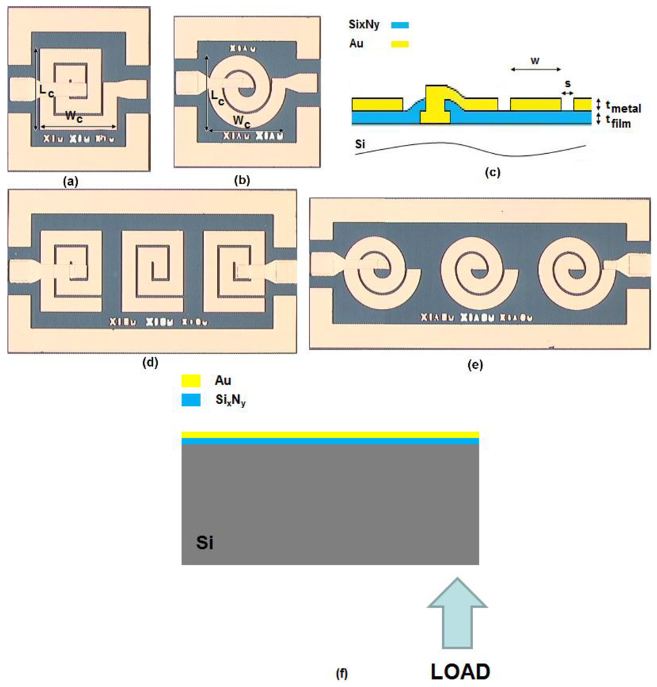
2. Design and Fabrication
For our resonators, we aim for a high Q-factor by using bio-compatible materials with a maximum possible resonance frequency shift. To design the resonator in a distributed spiral coil architecture with a high Q-factor (
Figure 1), we consider the effects of substrate, dielectric material, dielectric thickness (t
film), metal material, metal layer thickness (t
metal), metal width (w) and spacing (s), number of turns (N), and area (W
c × L
c) as explained in [
2]. Further details of the formulas and techniques for Q-factor enhancement can be found in [
4-
13]. For biocompatibility, we choose to use silicon as the substrate, gold as the metal layer, and Si
xN
y as the dielectric layer. Our main design strategy in achieving a maximum Q-factor with minimum spacing relies on the use of the distributed film capacitance as the LC tank circuit capacitance. The dominant parameter driving the resonance frequency shift is the on-chip capacitance change with mechanical deformation, allowing for strain measurement from the sensor without requiring additional circuitry. Although strain sensors using digital electronics [
14,
15] have been reported in the archival literature, the current work, to the best of our knowledge, represents the first account of an RF-based MEMS strain sensor in different architectures (circular geometries).
The following details using a circular architecture that better optimizes the aforementioned design aims. We compare two sensors with the same design parameters in rectangular and circular geometries shown in
Figure 1. In both cases, the total size (W
c × L
c) is 340 μm × 340 μm. In addition, both architectures have 2 turns (N), 60 μm wide metal width (w) and 10 μm wide spacing between coil segments (s). Their metal film thickness (t
metal) is 0.1 μm while their dielectric film thickness (t
film) is also 0.1 μm. The circular architecture has an effectively reduced total area compared to the rectangular geometry with the same dimensions. Thus, for the circular architecture, we obtain smaller film capacitance and coil inductance, yielding a higher f
o. Also, we have lower coil resistance, lower loss, higher substrate resistance, and lower substrate capacitance. This produces a higher substrate loss factor and self-resonance factor, which is discussed in detail in [
2]. As a result, with smaller spacing and higher f
o in the circular geometry, we achieve a higher inductor Q
ind-factor (and thus a higher resonator Q-factor).
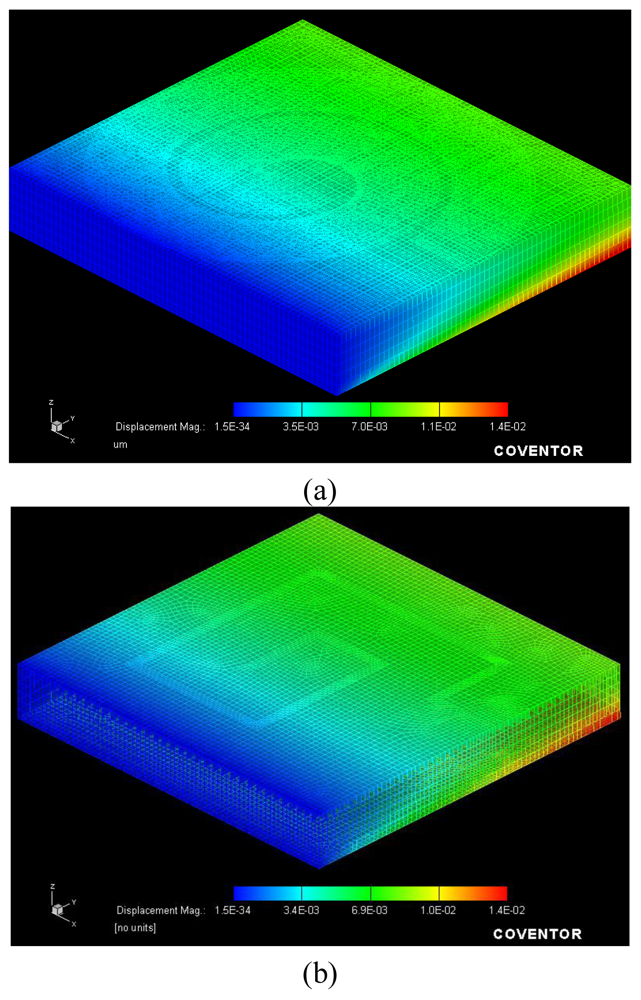
We approach the increase in the resonance frequency shift from two perspectives. First, the deformation is equally effective in any direction, thanks to the isotropic geometry as depicted in
Figure 2a. On the contrary, in a rectangular geometry, there is a preferential, anisotropic deformation, which dominates unilaterally (effective on only one side at a time) as illustrated in
Figure 2b. In
Figure 2, we can see that the maximum deformation of circular and rectangular shapes are the same but in rectangular geometry, one side is not deformed while in circular geometry, the whole geometry deformation is nearly the same. Therefore, the capacitance change in the circular case is higher than that in the rectangular case with the same starting initial capacitance value because the deformation acts to change the whole geometry. Hence, the associated resonance frequency shift is expected to be larger. Next, even if we have the same frequency shift ratio, Δf
o/f
o (relative shift), the frequency shift is higher in the circular geometry since it possesses a higher f
o. If we combine these two aspects, we have much higher shift for the circular case. Therefore, using the circular architecture, we expect to obtain a higher Δf
o and a higher sensitivity, e.g., defined as ∂f
O/∂F (or as ∂f
O/∂ε) with respect to the applied load (F) [or the induced strain (ε)]. Simulating S
21 parameters for the rectangular and circular devices and their triplet configurations, we also obtain higher resonance frequencies and higher Q-factors for the circular geometry. Thus, we predict better performance with the circular architecture.
For the implementation of our devices, our fabrication process begins with deposition and patterning of a 0.1 μm thick metal contact layer (Au) on the substrate (Si), and subsequent deposition of a 0.1 μm thick dielectric layer (Si
xN
y), a cross-sectional view of which is shown in
Figure 1c. We obtained the specific patterning with lithography and wet etching by hydrofluoric acid (HF). Subsequently, we metalized the open parts with 0.1 μm thick Au layer. Finally, another 0.1 μm thick final metal layer (Au) is deposited on top. The fabricated devices can be seen in
Figures 1a,b,d,e.
3. Experimental Characterization and Analysis
To characterize our fabricated devices, we apply a point load to our devices in a controllable manner using the same method as in [
3], where its schematic illustration is given in
Figure 1f, and measure the device S
21 parameter in response to the applied load. Thus, the change in resonance frequency and the Q-factor due to the applied load are determined. Our experimental set up includes an adjustable ultrafine-screw that can be adjusted to push towards the backside of the sensor. When the tip of this screw just touches the sensor backside, no load is applied, as verified by our reference strain gauge (made by Kyowa, Japan, with a gauge factor of 178). The screw is further twisted to apply load and induce strain. We confirmed the levels of strain induced with the position of the ultrafine-screw using our reference strain gauge.
For bioimplant sensing applications, there is an absolute requirement to measure and report strain remotely in the absence of wiring. Thus, for the current and future evaluations of this technology we need to measure and compare the telemetric performance of these sensors. To this end, we configure three resonators side by side on the same chip (in triplet configuration) and obtain an on-chip telemetry system. Although this on-chip system does not fully comply with the actual clinical application, it provides a robust methodology to compare different devices with respect to their telemetric operation. In this triplet configuration, the middle device serves as the sensor, with the lateral devices serving as the transmitter and receiver antennas. For calibration purposes, we measure the S
21 parameter of the case where there are only transmitter and receiver antennas, and then measure the S
21 parameters of our triplet configuration to obtain the resonance frequency and Q-factor. When the load is applied to the chip, the calibrations are again repeated with the same procedure as explained above to observe the changes in the resonance frequency and Q-factor. Also, using identical antennas guarantee to see the resonance frequency of the sensor since the working band of the antenna will definitely catch the resonance frequency of the sensor. Since the triplet method is used for easy coupling, using the antennas identical to the sensor makes our measurements further easier. A more detailed description of the triplet configuration operating principles is given in [
3].
The human body presents a more complex environment compared to the lab environment. This side-by-side testing scenario (in triplet configuration) is an idealized one, as this configuration provides merely an in vitro characterization platform. Having characterized the operation of these sensors in a side-by-side configuration, our future research work will include performing animal model experiments. We anticipate that there will be differences in the performance of our sensor when placed in the in vivo environment. Specifically, we expect reduced sensitivity levels due to the complex nature of the in vivo measurement medium. We also expect that the circular architecture will greatly enhance some of the proposed application areas for this sensor due to the significantly improved sensing performance of the circular designs.
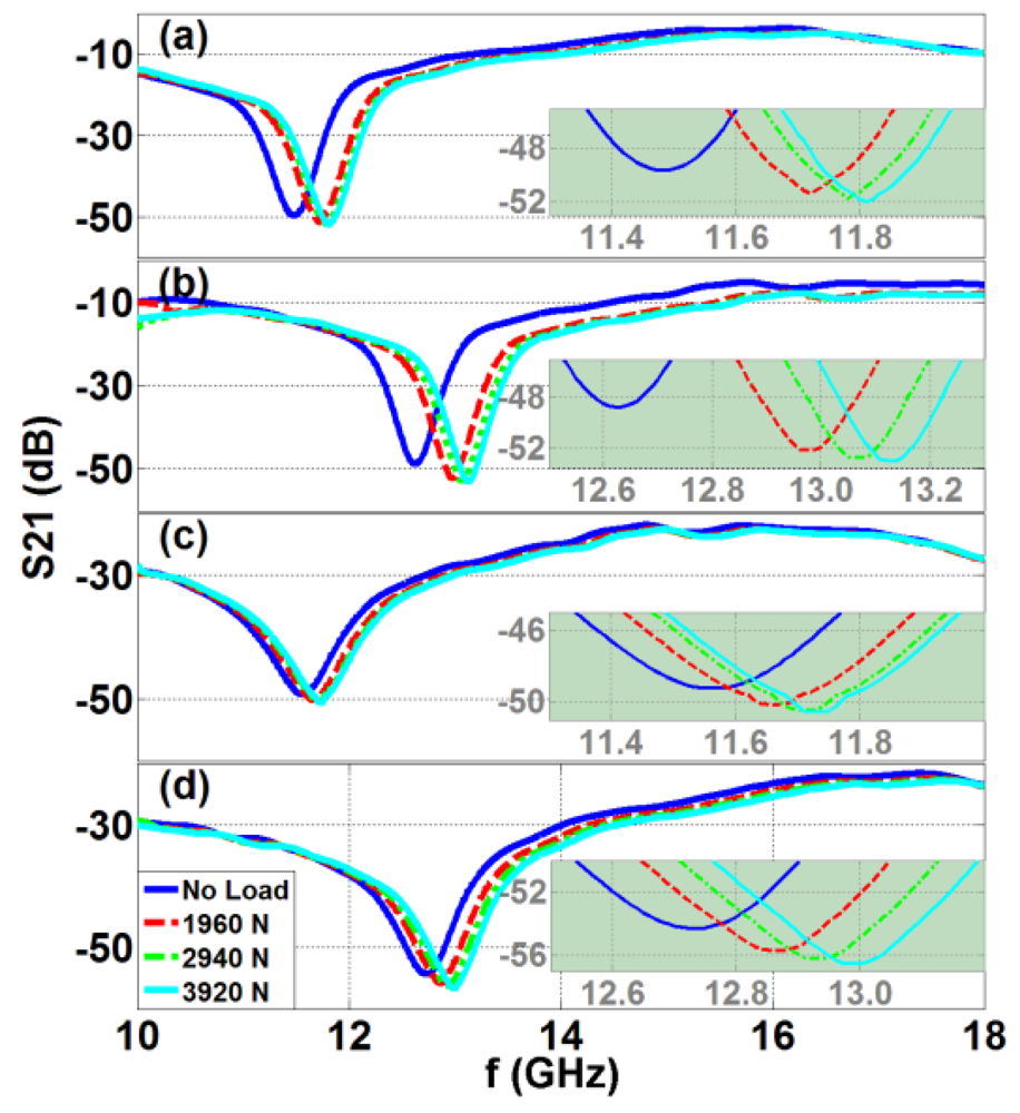
Figures 3a through 3d present S
21 (in dB) as a function of operating frequency for the single rectangular, single circular, triplet rectangular, and triplet circular configurations, respectively. All of these figures also include a zoom-in view (in the inset) of the data around the resonance frequencies.
Table 1 lists the measured resonance frequencies in response to the applied loading, clearly showing that the resonance frequency increases with the applied force due to decreasing area, and hence, decreasing capacitance. Also, all of these experimental S
21 data measured under zero external load are in agreement with our numerical simulations (in CST Microwave Studio).
In
Table 1, we also present the resonance frequency changes. The resulting resonance frequency increase is higher for all of the circular device geometries as explained above. Since the area decrease is not linear and the capacitance is not linearly proportional to the resonance frequency, the resulting frequency increase is expectedly nonlinear. In addition, since the frequency shift is much higher in the circular cases compared to the rectangular cases, we observe higher relative shift and higher sensitivity for the circular cases in
Table 1.
Table 1 also provides Q-factor data, which are observed to be high despite the relatively small chip sizes. These Q-factors are particularly higher in the circular case with a smaller area. The Q-factor is increased as the load magnitude is increased due to a lower C
film, as discussed in [
2] and [
3]. The Q-factor also increases for the telemetric case of the circular case compared to the rectangular case. However, in the telemetric operation, due to coupling between resonators, the signal is decreased and Q-factors are reduced for both of the rectangular and circular cases compared to the single device cases. Our experimental apparatus can reproducibly apply a minimum strain of 81.5 microstrain, while the maximum strain is 172.8 microstrain. Therefore, it is not possible to make a direct measurement of the minimum detectable strain level for our sensors. Since the resolution of the network analyzer that we use in our experiments is 1 Hz (given the typical noise level in our experiments), we find the resolution of our sensors in the strain range across which they are tested by dividing this minimum detectable frequency to their sensitivities. From this calculation, we obtain 526.3 femtostrain for single rectangular device and 344.8 femtostrain for single circular device. These resolutions are better than those reported in [
15].
Another interesting point for discussion is the hysteresis behavior. When different levels of external load are successively applied without allowing the mechanical setup to fully relax into the new loading conditions (typically in a time scale of minutes), we observe a memory effect and see a hysteresis in the experimental characterization of these sensors. The sensors in circular geometry exhibit a wider hysteresis loop as expected because they are more sensitive sensors, compared to those in the rectangular geometry. However, if one waits long enough (minutes) between successive force levels, no hysteresis is observed. The experimental data presented here is for the case of no hysteresis.


