Article

Photo-Induced Unpinning of Fermi Level in WO3

1
Department of Physics University of Ferrara, Via Saragat 1c, 44100 Ferrara, Italy
2
INFN Section of Ferrara, Italy
3
Chemistry and Physics Department, Brescia, Italy
4
University of Wales Swansea, Swansea, UK
*
Author to whom correspondence should be addressed.
Sensors 2005, 5(12), 594-603; https://doi.org/10.3390/s5120594
Submission received: 6 October 2005 / Accepted: 19 December 2005 / Published: 20 December 2005

Abstract

:
Atomic force and high resolution scanning tunneling analyses were carried out on nanostructured WO3 films. It turned out that the band gap measured by scanning tunneling spectroscopy at surface is lower than the band gap reported in the literature. This effect is attributed to the high density of surface states in this material, which allows tunneling into these states. Such a high density of surface states pins the Fermi level resulting in modest surface activity at room temperature. Photo activation of WO3 results in unpinning of the Fermi level and thereby in higher chemical activity at surface.

1. Introduction

WO3 is a widely studied material owing to its established photochromic and electrochromic properties [1]. The electrical properties of nanostructured WO3 have emerged since about a decade, with the demonstration of its gas sensing characteristics, especially for detection of oxidizing agents [2]. As for most metal oxides, the chemoresistive properties of such material appear on the strength of its nanostructured nature. In fact, below a certain threshold for grain size, the sensing properties of n-type metal oxides appear to be magnified [3] at usual working temperatures, i.e., from 150°C to 450°C. Thus the determination of a characteristic length below which a material can be regarded as nanostructured is crucial. As for the most widely used SnO2, the sensitivity of WO3 to gases is almost independent [4] of grain size above 40-50 nm. Unlikely, TiO2 shows very different behavior in the same range of grain dimensions [5]: its sensitivity appears to depend strongly on the grain size up to 150 nm. A work appeared elsewhere [6] and its recent development [7] proposed a model to explain this effect in terms of pinning/unpinning of the Fermi level operated by surface states by virtue of their dependence on grain size.
In addition, it has been recently demonstrated that WO3 exhibits sensitivity to environmental changes when stimulated by light [8]. Such effect can be profitably employed for gas sensing at room temperature, an extensively pursued application over the last years. Although a clear experimental scenario is known from the literature, no net understanding of the physics behind this phenomenon has been given yet.
We adapted the mentioned model to provide an interpretation of WO3 photo-activation. It turned out that photo-activation plays the same role as size reduction in the case of TiO2, i.e., it controls the switch from pinning to unpinning of the Fermi level and, in turn, determines a change in the chemoresistive properties of WO3.

2. General background

When dealing with semiconductor-gas interfaces, an insight into the fundamental mechanisms of barrier formation at gas-semiconductor interfaces is needed. The surface barrier, Sb, has the following form [9]:
S b = X φ
with X the work function, and ϕ the electron affinity. X is strongly affected by the amount of surface species chemisorbed from the environment. Therefore its variation quantifies the strength of the interaction between the semiconductor and the surrounding gas.
According to Bardeen's theory [10], the strength of a double layer of atomic dimension at the semiconductor surface plays a role comparable to that of space charge in determining the work function. Indeed, for the limiting case of a very high density of surface states, the work function of a free semiconductor surface is determined by the energy position of the neutral level [10] with respect to the conduction band minimum, εo, as follows:
X = φ + ε o
If the density of states is high enough, any variation of X can be compensated for by either a variation of the electron affinity due to surface dipoles [9] or a rearrangement of the surface charge, rather than by a variation of the surface barrier. This situation, expressed by Eq. 2, is referred to as pinning of the Fermi level. In fact, as the density of charged surface states is sufficiently high, from Eqs. (1) and (2) it turns out that the surface barrier has the constant value εo. Therefore, a variation of the amount of surface states, which can be induced by surface reactions, does not result in a corresponding surface barrier variation. Under such condition the material is almost insensitive to environmental changes.
When the density of states decreases, only Eq. (1) holds and a variation of X involving charge transfer will result in appreciable variation of Sb. This phenomenon is the so called unpinning of the Fermi level and results in larger sensitivity of the material to environmental modifications.

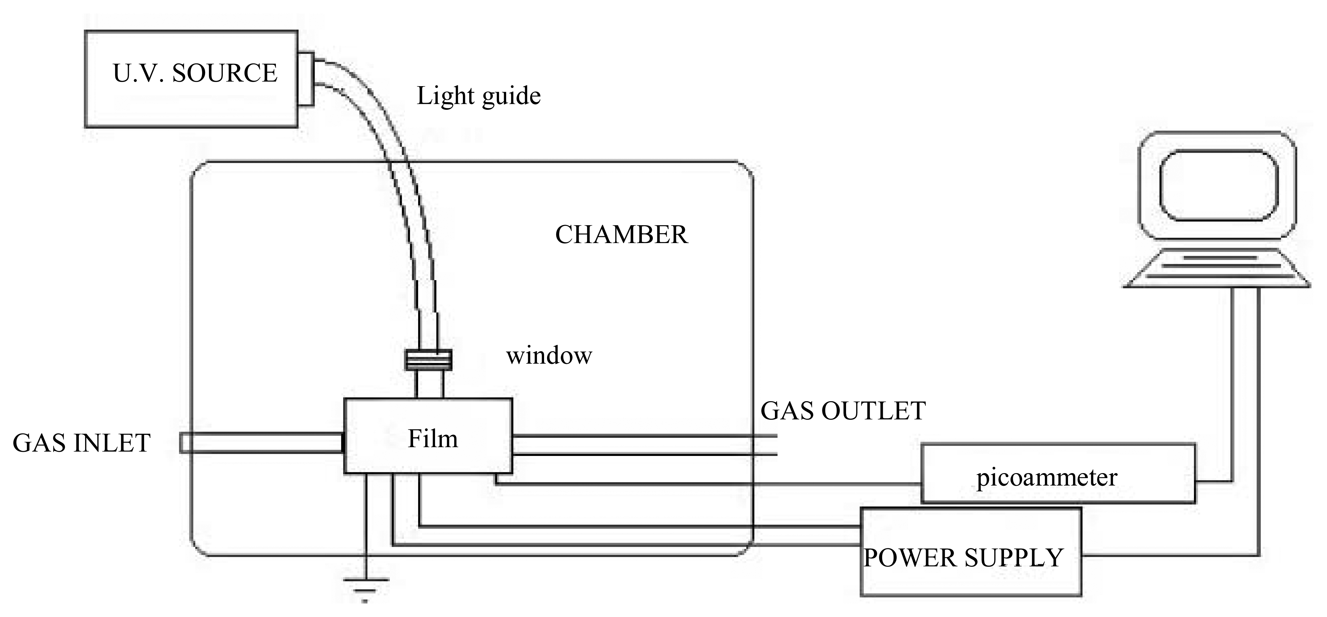
3. Experimental Section

Tungsten oxide thin films were prepared by reactive magnetron radio frequency sputtering. The deposition has been performed starting from a metallic target with certified purity at 99.99% in an oxidizing atmosphere with 50% argon and 50% oxygen at a working pressure of 8×10⁻³ mbar. During the deposition the substrate is maintained at 300°C to favor the formation of a stable layer and, after the deposition, the deposited layer underwent an annealing cycle at 450°C for 12 hours to guarantee the stability of the films during the operation over a wide range of temperatures. Annealing was performed in a furnace under controlled flux of humid synthetic air. WO3 tends to suffer from exaggerated coalescence on annealing, therefore a moderately low annealing temperature was imparted. Temperature was measured by a thermocouple placed on the internal wall of the furnace. For the electrical characterization, the films were deposited onto 3×3 mm2 wide 250 μm thick Al2O3 substrates equipped with a Pt meander heater on the backside; Pt interdigitated contacts were sputtered onto the thin-film side for electrical measurements.
Conductance measurements were performed by the flow-through technique as a function of the temperature and gaseous environment with a 0.3 l/min flow of humid synthetic air (RH 30%). The gas test measurements were performed both with photo-activation and in dark conditions. In the first case, the films were exposed to an UV Hg-Xe lamp (Hamamatsu SuperQuiet Mercury Xenon lamp) coupled with a fiber (see Fig.1). The energy spectrum of the emitted radiation is the superposition of Xe and Hg spectra, the principal peak is at 365 nm, an optical filter cut all the frequency apart from 240 to 400 nm. The maximum incident power value was 26.2 mW/mm2 measured at the end of the fiber.
The scanning tunneling microscopy (STM) and STS investigations, as well as the high resolution contact AFM imaging were performed in ultra high vacuum (UHV) using an Omicron VT AFM-STM system (base pressure 10-11 mbar). The STM probe tips were fabricated by electrochemical etching of tungsten wire.

4. Results and discussion

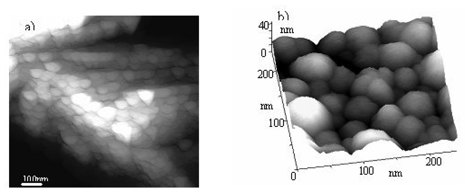
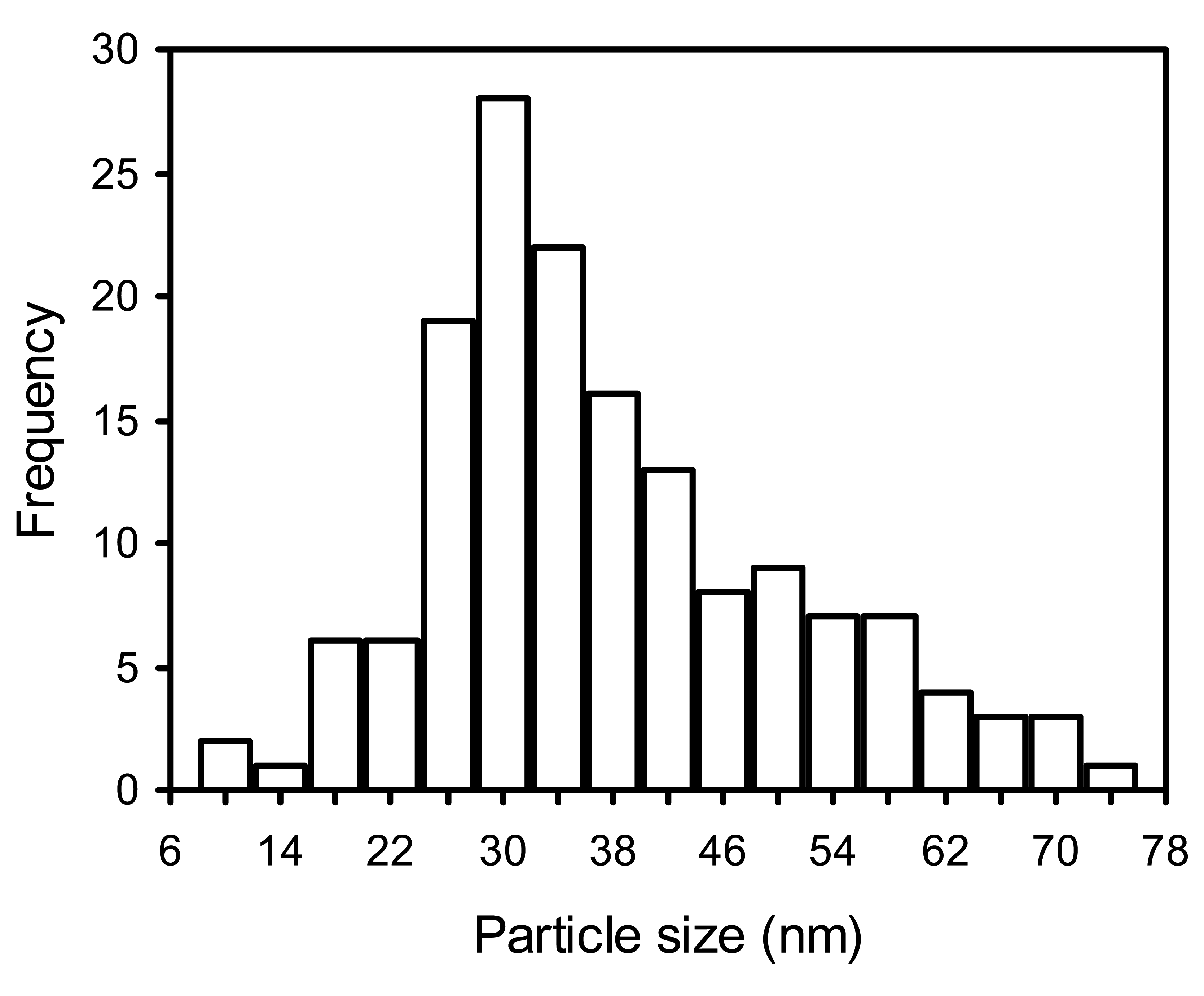
4.1. Investigation by electron microscopy techniques

A SEM image of a WO3 film deposited via RF sputtering is shown in Fig. 2 (a) and compared with an AFM image (Fig. 2 (b)). The film shows a compact and homogeneous morphology, possibly thanks to the deposition technique. To investigate the surface more deeply, down to the nanometric level, we placed the sample in our UHV AFM-STM system. High resolution contact AFM and STM images are shown on Fig. 3 a) and b). The AFM image reveals the presence of grains with a size of a few 10's of nanometers. The porosity of the structure can be observed as well as the mean grain size on the close-up STM image (Fig. 3b). The distribution of grain diameters, obtained from several STM images, peaks at approximately 30 nm and averages at 42 nm (see Fig. 4). This dimension is sufficiently larger than WO3 depletion width not to have surface state density dependence on grain size. The distribution appears to be asymmetric since coalescence of largest particles is achieved at the expense of neighboring smallest ones. The spherical shape of the particles represents further evidence of the absence of a secondary coalescence mechanism. Through scanning tunnelling spectroscopy (STS) technique, it is possible to determine the density of the surface states that are responsible for pinning of Fermi level. In fact, narrowing of the measured band gap, is expected for a semiconductor in which the surface density is very high, due to tunneling of electrons in the forbidden region owing to these states. The band gap reported in the literature for WO3 films obtained with a similar method of deposition is 3.05 eV [11].
STS curves were recorded simultaneously with the STM images at three different tip-sample separations, determined by tunneling current setpoints of 1nA, 0.1nA and 0.01nA. In this configuration, the tip stops scanning and the feedback loop is turned off before acquisition of a current versus sample bias curve (I(V)), and the tip-sample separation during acquisition is fixed by the current setpoint used during scanning. The separation increases as the current setpoint decreases. The results are sketched in Fig. 5. Fig 5a) shows the I(V) curves at three different tip-sample separation, while Fig 5b) shows a Log(I) versus V plot of the same curves. The increase in current is evident as the tip-sample separation is lowered. Fig 5c) shows a plot of the normalized conductivity (dI/dV)/(I/V) derived from the three curves. The normalized conductivity is a good representation of the density of surface states [12] and clearly shows features between −2V and 1V on indication of surface states within the band gap. These surface states make it difficult any precise determination of the band gap. Indeed, as the tip sample separation is decreased (from 0.01nA to 1nA current setpoints) the tunneling current originating from the surface states increases and the apparent surface band gap appears to be very small (<0.1 eV).

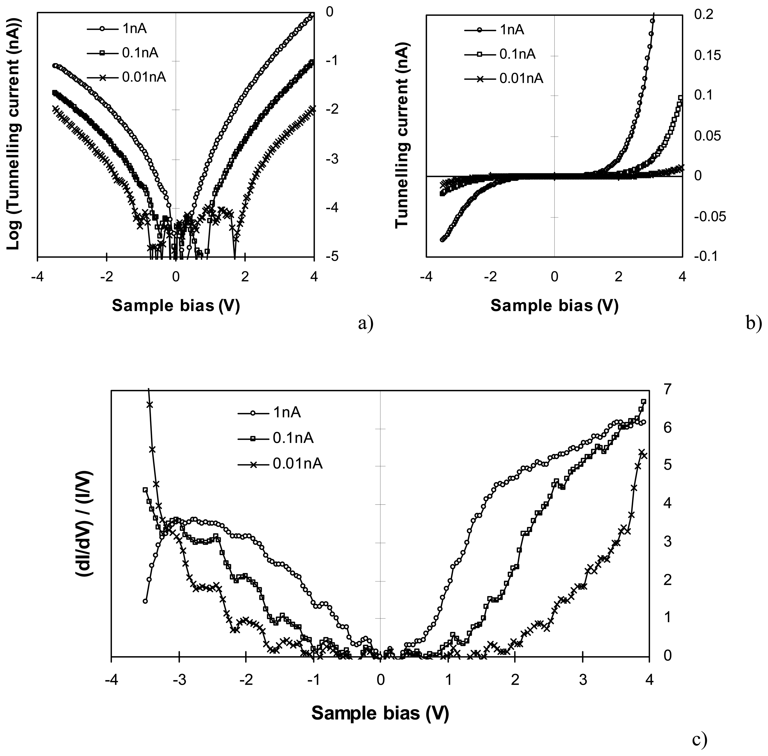
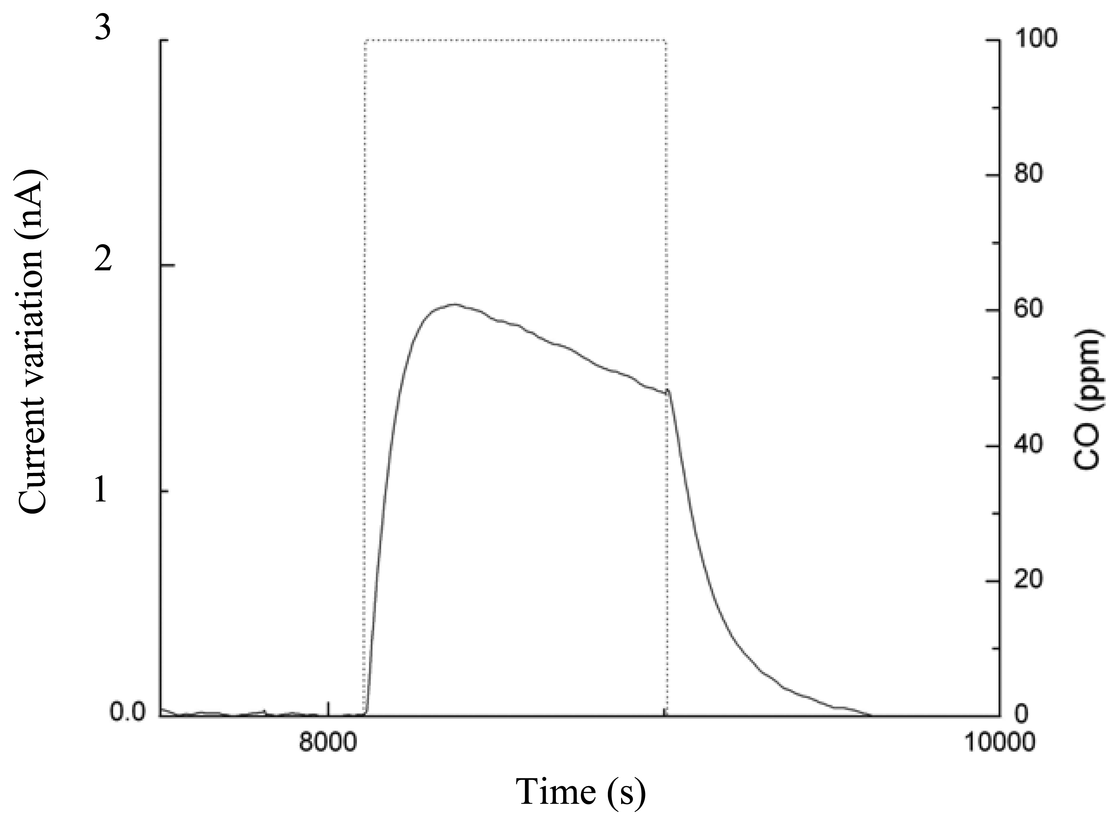
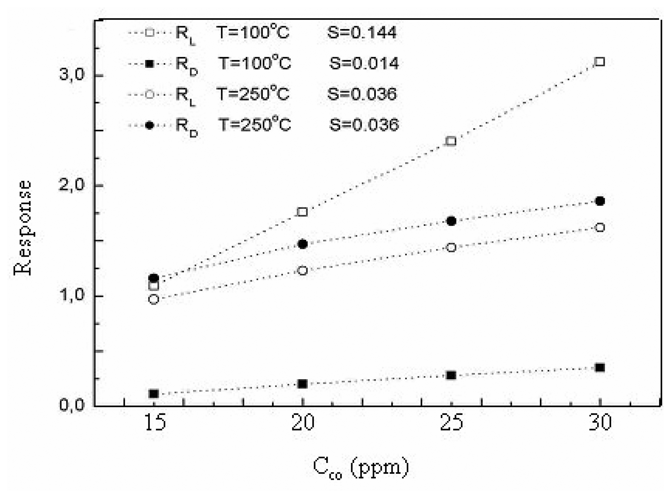
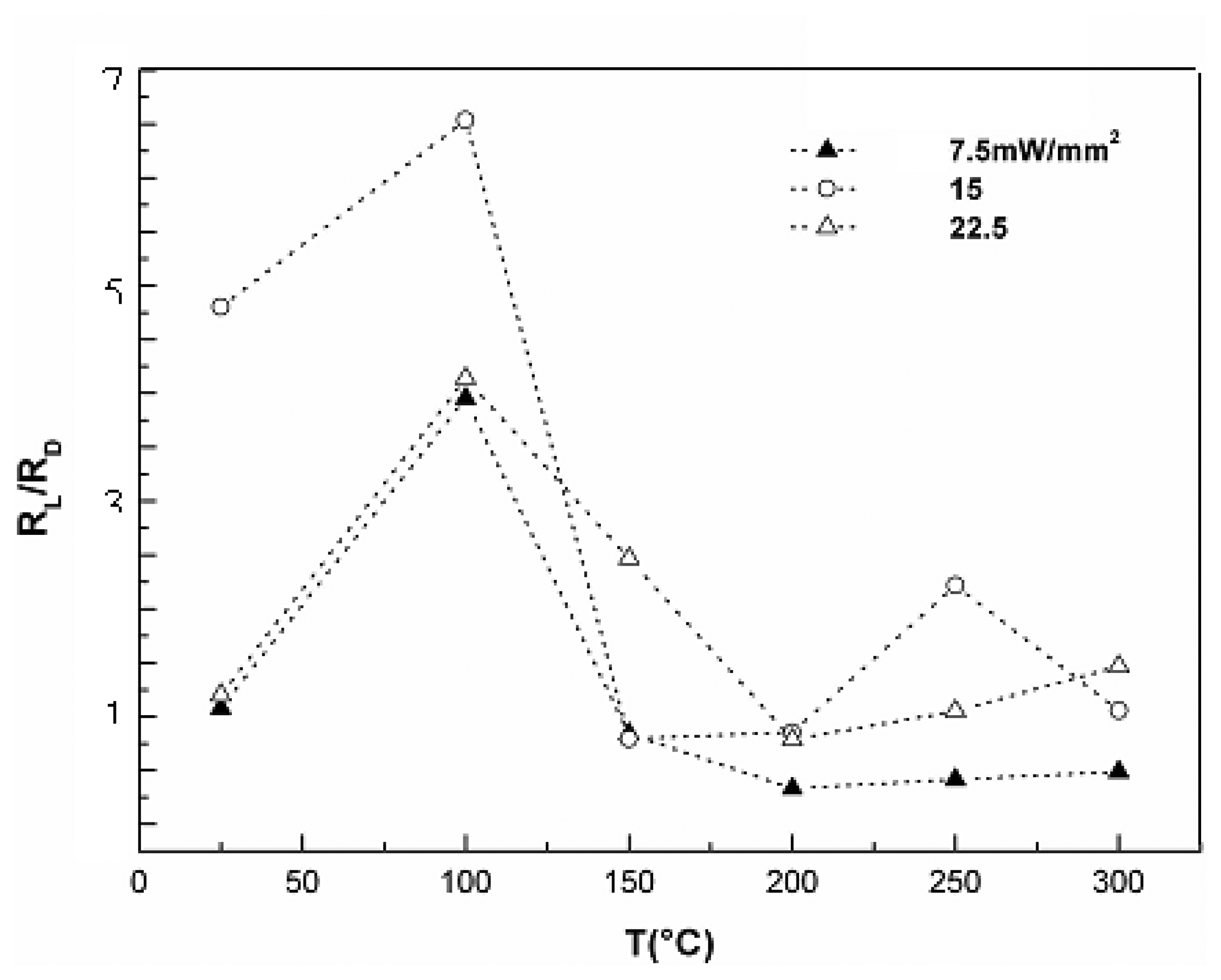
4.2. Investigation by photoactivation

Pinning of the Fermi level is effective as the density of surface states is high enough (Ns>1012cm-2) to form a considerable surface layer [10]. Modification of the environment of the semiconductor represents a useful tool for studying this phenomenon. The molecules of a gas may interact, in fact, with the surface of the semiconductor with charge exchange (chemisorption). It is known from the literature [13] that the resistance of a metal-oxide semiconductor is strongly influenced by such interaction. Indeed, as the pinning of the Fermi level occurs, a very little variation of resistance is observed even if the environment is significantly altered.
We used CO as a target gas, which is a reducing species of great importance for air-quality monitoring in urban areas. Carbon monoxide reacts with oxygen species chemisorbed on the semiconductor (O2-, O-, O2-) with a consequent increase in conductance; as an example, for O- a possible reaction is:
CO + O CO 2 CO 2 + e
Concentrations of CO lower than or equal to 100 ppm were used for the experiment described in this work, which are in the range of interest for environmental application, aiming at a possible sensoristic use of the films. In Fig. 6 an example of a dynamical response of a film to 100 ppm of CO is reported: the voltage is kept fixed, thereby an increase in current represents an increase in conductance. The conductance of the layers rises up when CO is fed into the test chamber; this behavior is normal for an n-type semiconductor due to release of electrons in the conduction band of the semiconductor.
Following the literature, the response of the sensor toward a gas is defined as the normalized variation of conductance (RG/G0 = (G-G0)/G0, where G and G0 are the conductance when a test gas is present and when it is not, respectively). The dependence of the response on concentration follows the established [13] power law for metal-oxide semiconductors, R=A+B×CCOα, A, B and α being constants and CCO the concentration of CO. RD (RL) is the value of the response without (with) UV exposure.
Fig 7 shows the response with light (15 mW/mm2) and in the dark as a function of CO concentration, at two operating temperatures. The curves are power laws, which confirms that chemisorption, and not physisorption is the main phenomenon involved under all conditions. The related values of sensitivity, SRCCO, are reported in the legend. Sensitivity is increased ten times by UV irradiation at the lower temperature, whereas it is unaffected by light at the higher temperature.
To clarify this behavior, we report in Fig. 8 the ratio between RL and RD as a function of temperature at three different values of incident power, towards 100 ppm of CO. As can be noticed, the enhancement of the performance of the sensing layer due to light tends to be stronger at lower temperatures. In particular, the ratio RL/RD is maximum at 100°C, and decreases at higher temperatures, independently of the intensity of the incident light.
The experimental evidences can be interpreted in terms of pinning and unpinning of Fermi level: at relatively low temperature the large amount of charged surface states pins the Fermi level, thus determining nearly a zero band gap and poor response to environmental changes. The increase in the response while illuminating is due to light-induced unpinning.
At higher temperatures, thermal effects control the response to CO. Here, any further stimulation by light causes negligible effect.

5. Conclusions

Morphological and electrical characterizations have been carried out for WO3 sputtered thin films. The band gap in the bulk resulted sensibly larger than the band gap at surface. The narrowing of the surface band gap is attributed to a high density of surface states, such as chemisorbed O2-, from which tunneling current originates in the forbidden region as revealed by STS. Surface states pin the Fermi level at low temperature; illumination with UV radiation promotes unpinning of the Fermi level and increases the response to environmental changes. This investigation also highlights great potential for sensing CO via photo-assisted reactions. Therefore, the need for operation at relatively high temperatures, which is a well documented disadvantage of metal oxide based gas sensors, can be circumvented.

Acknowledgments

We gratefully acknowledge the European Union for funding the NANOS4, INFM PON SVISENARIA and INFN DEGIMON projects.

References

  1. Granqvist, C.G. Handbook of Inorganic Electrochromic Materials; Elsevier: Amsterdam, 1995. [Google Scholar]
  2. Faglia, C.; Baratto, C.; Sberveglieri, G.; Zha, M.; Zappettini, A. Adsorption effects of NO2 at ppm level on visible photoluminescence response of SnO2 nanobelts. Appied Physics Letters 2005, 86, 11923–11925. [Google Scholar]
  3. Shimizu, Y.; Egashira, M. Basic Aspects and Challenges of Semiconductor Gas Sensors. MRS Bulletin 1999, 24, 18–24. [Google Scholar]
  4. Blo, M.; Carotta, M.C.; Galliera, S.; Gherardi, S.; Giberti, A.; Guidi, V.; Malagù, C.; Martinelli, G.; Sacerdoti, M.; Vendemiati, B.; Zanni, A. Synthesis of pure and loaded powders of WO3 for NO2 detection through thick film technology. Sensors and Actuators B 2004, 103, 213–218. [Google Scholar]
  5. Bonini, N.; Carotta, M.C.; Chiorino, A.; Guidi, V.; Malagù, C.; Martinelli, G.; Paglialonga, L.; Sacerdoti, M. Doping of a nanostructured titania thick-film: Structural and electrical investigations. Sensors and Actuators B 2000, 68, 274–280. [Google Scholar]
  6. Malagù, C.; Guidi, V.; Stefancich, M.; Carotta, M.C.; Martinelli, G. Model for Schottky barrier and surface states in nanostructured n-type semiconductors. Journal of Applied Physics 2002, 91, 808–814. [Google Scholar]
  7. Malagù, C.; Guidi, V.; Carotta, M.C.; Martinelli, G. Unpinning of Fermi level in nanocrystalline semiconductors. Applied Physics Letters 2004, 84, 4158–4160. [Google Scholar]
  8. Comini, E.; Cristalli, A.; Faglia, G.; Sberveglieri, G. Photo activation in gas sensors: a new method to reduce the working temperature. Proc. 7th IMCS, Beijing, China, 27–30 July 1998; pp. 509–511.
  9. Barsan, N.; Weimar, U. Conduction Model of Metal Oxide Gas Sensors. Journal of Electroceramics 2001, 7, 143–167. [Google Scholar]
  10. Bardeen, J. Surface States and Rectification at a Metal Semi-Conductor Contact. Physical Review 1947, 71, 717–727. [Google Scholar]
  11. Miyake, K.; Kaneko, H.; Teramoto, Y. Electrical and optical properties of reactively sputtered tungsten oxide films. Journal of Applied Physics 1982, 53, 1511–1515. [Google Scholar]
  12. Feenstra, R.M. Electronic states of metal atoms on the GaAs(110) surface studied by scanning tunneling microscopy. Physical Review Letters 1989, 63, 1412–1415. [Google Scholar]
  13. Morrison, S. R. The Chemical Physics of Surfaces; Plenum Press: New York, 1977. [Google Scholar]
Figure 1. Experimental apparatus for photo-activation measurements.
Sensors 05 00594f1
Figure 2. a) SEM image of WO3 deposited via RF sputtering. b) AFM image of the same sample.
Sensors 05 00594f2
Figure 3. a) High resolution 1000×1000nm2 contact AFM image acquired at a force setpoint of 20nN. The grey scale corresponds to a z-range of 140nm. b) 3D 250×250nm2 constant current STM image acquired at a tip voltage of 3V and tunneling current setpoint of 0.6nA.
Sensors 05 00594f3
Figure 4. Particle size distribution extracted from STM images.
Sensors 05 00594f4
Figure 5. a) current versus sample bias curves acquired at three tip-sample separations. b) semi log plot of the three I(V) curves and c) (dI/dV)/(I/V) versus V spectra derived from the three I(V) curves. The high density of surface states induces an apparent reduction of surface band gap with respect to the bulk value.
Sensors 05 00594f5
Figure 6. Dynamical response to a square pulse of 100 ppm of CO. Current rises up due to redox reactions at surface. The characteristic response time of a layer is visible.
Sensors 05 00594f6
Figure 7. Response with light (15 mW/mm2) and in dark conditions as a function of CO concentration and sensitivity, SRCCO.
Sensors 05 00594f7
Figure 8. Ratio between the response (ΔG/G) toward 100 ppm of CO with light activation (RL) and in dark conditions (RD) as a function of the operating temperature and with different UV incident power. The best conditions for an increase in performance of the sensor are 100°C as operating temperature and 15 mW/mm2 as incident UV power on the sensor.
Sensors 05 00594f8

