Article

Electrical and Physical Characteristics of WO3/Ag/WO3 Sandwich Structure Fabricated with Magnetic-Control Sputtering Metrology

1
Department of Materials and Resources Engineering, National Taipei University of Technology, Taipei 10608, Taiwan
2
Department of Electronic Engineering, Minghsin University of Science and Technology, Hsinchu 30401, Taiwan
3
Chung-Shan Institute of Science and Technology, Taoyuan 32546, Taiwan
*
Author to whom correspondence should be addressed.
This paper is an extended version of our paper published in 7th International Symposium on Next Generation Electronics (ISNE 2018), Taipei, Taiwan, 7–9 May 2018.
Sensors 2018, 18(9), 2803; https://doi.org/10.3390/s18092803
Submission received: 2 August 2018 / Revised: 19 August 2018 / Accepted: 22 August 2018 / Published: 25 August 2018

Abstract

:
In this work, three layers of transparent conductive films of WO3/Ag/WO3 (WAW) were deposited on a glass substrate by radio frequency (RF) magnetron sputtering. The thicknesses of WO3 (around 50~60 nm) and Ag (10~20 nm) films were mainly the changeable factors to achieve the optimal transparent conductivity attempting to replace the indium tin oxide (ITO) in cost consideration. The prepared films were cardinally subjected to physical and electrical characteristic analyses by means of X-ray diffraction analysis (XRD), field-emission scanning electron microscope (FE-SEM), and Keithley 4200 semiconductor parameter analyzer. The experimental results show as the thickness of the Ag layer increases from 10 nm to 20 nm, the resistance becomes smaller. While the thickness of the WO3 layer increases from 50 nm to 60 nm, its electrical resistance becomes larger.

1. Introduction

The transparent conductive film (TCF) offers versatile and cost-effective applications with a light transmittance of 80% or more in visible light range (400 to 800 nm) and low resistivity [1], sometimes treated as optical or electrical sensors [2,3,4]. With the rapid expansion of the market for photovoltaic elements, the demand is rapidly increased, so is the pursuit of high stability and low cost processes in production. The transparent conductive film should exhibit both transparent and conductive properties. Currently, most of the materials are metal oxides, called transparent conducting oxides (TCO), especially with indium tin oxide (ITO) [5]. It was found that ITO material can be employed as an ohmic contact layer [6]. However, the “indium” element in indium tin oxide is a rare metal and expensive, so that many manufacturers and research institutes in the world are proactively developing the ITO-like materials to replace the previous. It was found that if a metal layer was added to the conductive film to form a multilayer film structure, the overall conductivity and mechanical properties of the film were possibly and greatly increased instead of ITO. Depositing a suitable metal thickness in a clamping oxide structure seems possible in the recent development stage, without affecting the visible light transmittance while still maintaining its low-resistance properties. This is also the aim of this work; to make an acceptable cost-effect TCF in future applications.
Most of metal thin films such as Au, Ag, Cu, Pt, and Al are, basically, good infrared reflectors. If the optical transparency in the tunable region is strongly enhanced, the preferred thickness of the metal film layer is less than 10–20 nm. Theoretically, the metal thin film can be treated as a good transparent conductive film, but when the thickness of the metal thin film is less than 10 nm, it is easy to form discontinuous island-like films, so that the resistivity of the thin film increases and the scattering incidence light in turn reduces the transparency of the film itself [1]. Metal oxide films have a long history of application to TCO, and cadmium oxide (CdO) was first prepared by sputtering in 1907 by Badeker. In 1954, Rupprecht vapor-deposited metal indium (In) onto a quartz substrate and oxidized it at 700 to 1000 °C in an atmosphere (oxygen: nitrogen = 1:4) to obtain transparent and conductive indium oxide (In2O3). Furthermore, it is inferred that the conductivity of this film is a crystal defect derived from the film structure itself. In 1968, Philip found that the doping of Sn ions in the indium oxide film enhanced the conductivity of the overall film, and then produced In2O3:Sn film [7], now widely consolidated in indium tin oxide [8,9,10] applications.
The transparent conductive oxide of the metal is transparent in the visible region. For electrical properties, these oxides are usually doped with some metal impurities, doped with metal ions that are more than one cation of the original compound to form an n-type semiconductor, or doped with a non-metal ions less than its anion to form a p-type semiconductor. It is also probable to generate a compound having an incomplete oxidation state, so that an anion void is contained in the material, and WO3 according to the present experiment is usually an n-type semiconductor material and has a work function (Φs) around 5.7 V.
Among many metal materials, silver (Ag) material is a good choice in conductivity and relatively good photoelectric characteristics. Accompanying tungsten oxide (WO3), a semiconductor material with a large energy gap, it has a chance to form a transparent conductive film mainly composed of tungsten oxide and a silver metal layer in the middle. According to different characteristics of the WO3/Ag/WO3 transparent conductive film, it is expected to develop different application components and products in the future. Tungsten oxide (WO3) generally proposes a molecular weight of 231.838 g/mol, a density of 7.2 g/cm3, and a melting point of about 1473 °C and is soluble in water and ammonia, but slightly soluble in hydrofluoric acid, and, however, insoluble in acid. Tungsten compounds can usually exhibit five different ionization states, W2+, W3+, W4+, W5+, and W6+. There are also cases where codons of different valences coexist. WO3 is the highest valence oxide of tungsten. As usual, the oxygen content in tungsten oxide does not exactly meet the full stoichiometric ratio of O:W = 3:1, so that the chemical formula is often expressed as WO3−x. The conductive mechanism of the tungsten oxide is chiefly via oxygen vacancies. Oxygen vacancies are mainly formed because of the large number of tungsten oxides arranged, and the oxygen atoms in the structure are vacant due to defects in the material itself. In this case, the chemical formula of tungsten oxide should be WO3−x, and the sporadic oxygen vacancies will generate a new energy level below the conduction band. At the generated energy level, the active electrons are able to be transited to the upper energy levels. The conduction band generates free electrons and is thus electrically conductive [5].
As shown in Figure 1, the valence band of WO3 is composed of O atoms 2s, 2p orbitals, and the conduction band is composed of W atoms 5d orbitals. According to the crystal field theory, the 5d orbital division of W is separated into two parts, eg and t2g, but they are all unfilled orbits. Therefore, the WO3 valence band is cardinally localized in the O(2p) orbital, the conduction band is localized in the t2g orbital of the central metal W6+, and the Fermi level is between the O(2p) band and the W(t2g) band [8,11,12,13,14]. The other possible formation of tungsten oxide, as shown in Figure 2, is WO2. The Fermi level (EF) of WO2 is generally in the conduction band, so that active electrons do not need much energy to look for the quantum state of the vacancy for jumping and inducing current conduction. The bandgap of WO2 is not remarkably observed.

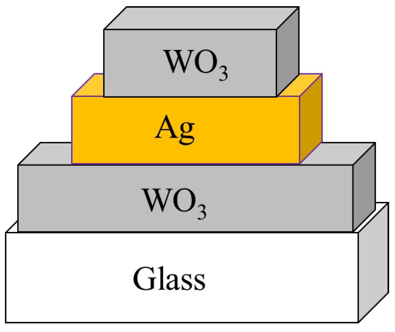
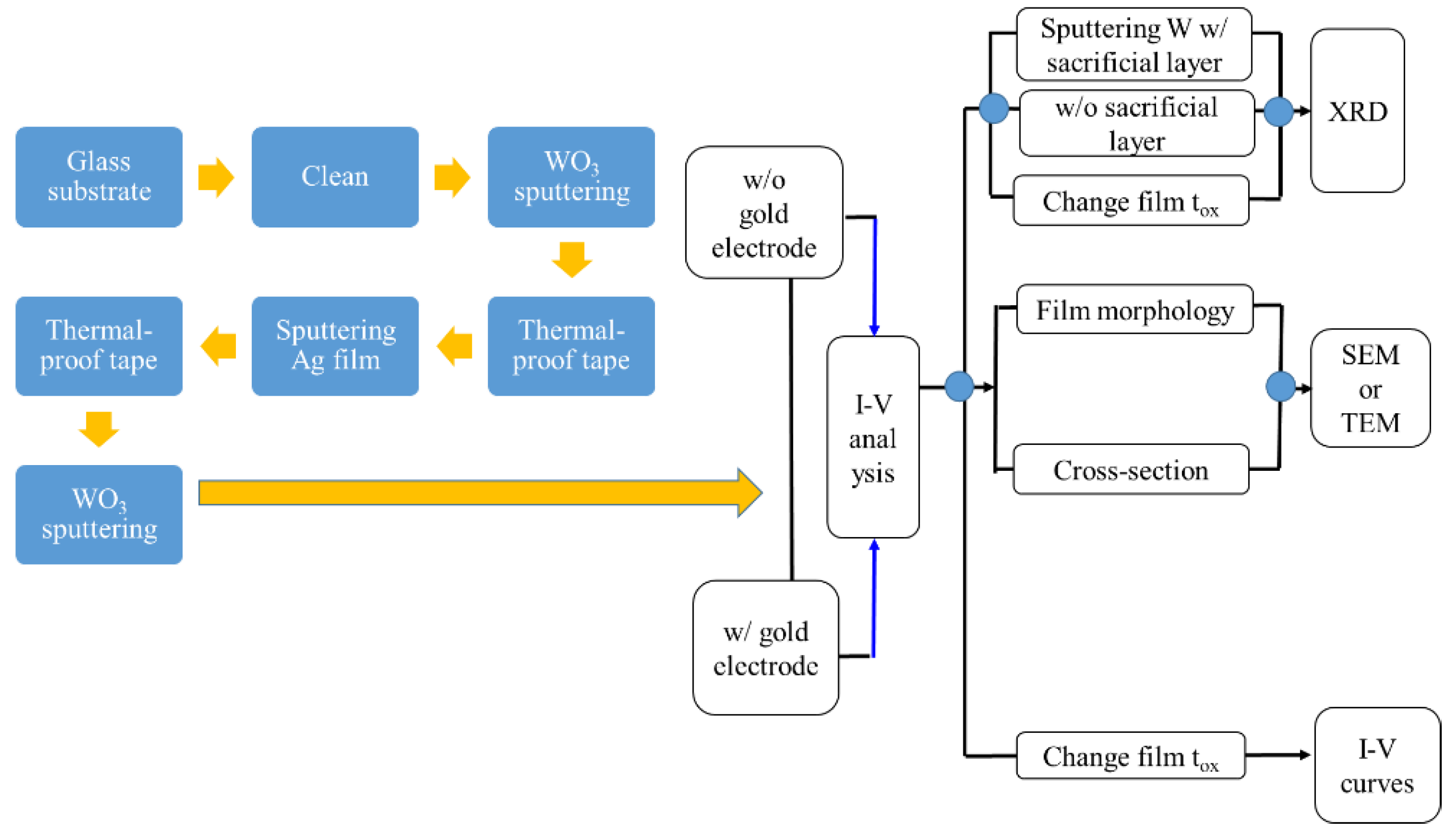
2. Fabrication of WAW Conductive Films

The chosen substrate in this work is a glass substrate, which is a level of sodium glass. The selected target of tungsten is a 2-inch circle type with the integrity 4N. In the experiment, the flowing gases are pure argon and oxygen. Before the sputtering, the glass substrate must be cleaned well with acetone, de-ionized (DI) water, and alcohol in the operation of ultra-sonic equipment. After that, the de-dry process with nitrogen is subsequently executed. Before the beginning of sputtering, the glass substrate required for the experiment must be cleaned, placed in a beaker containing acetone, deionized water, and alcohol, and then in an ultrasonic oscillator for 10 min. The function of acetone is to remove the organic matters on the surface of the substrate. Deionized water can take out the dust and chemicals on the substrate surface. Alcohol takes the surface moisture of the substrate away. After cleaning, the residual alcohol on the surface of the glass substrate should be fully dried out by a nitrogen gun.

2.1. WAW Film without Plated Electrode

After the cleaned substrate was placed in the sputtering chamber, the magnetron sputtering system was step by step turned on for sputtering, following the standard operation procedures, and the mechanical pump was used to pump the chamber. When the pressure of the chamber reached 0.05 torr, the diffusion pump was added and pumped up to the background pressure of 2 × 10⁻⁵ torr for tungsten oxide deposition the gas introduced into the chamber was argon (flow rate: 30 sccm) and oxygen (flow rate: 24 sccm), and the working pressure was 7 × 10⁻³ torr. For deposition of a silver layer, the gas was argon (flow rate: 30 sccm), and the working pressure was 6 × 10⁻³ torr, and the tunable rotation speed was set to 300 rpm. Subsequently, the metal target must be pre-sputtered for 15 min before the start of sputtering to remove impurities from the target surface. After the plasma environment stabilized, the baffle between the target and the stage was slowly removed, and the procedure of film deposition was begun. Continuously, after the sputtering completed, the test piece was taken out. Ultimately, the plating analysis and the property test for the deposited films were performed. During the sputtering process, the thicknesses of the silver (10 or 20 nm) and the tungsten oxide (50 or 60 nm) and the RF power to generate the plasma were the main changeable factors, as shown in Table 1. Pre-sputtering the surface of the target for 15 min was to remove the surface impurities and oxide layer to clean the target surface well. After the pre-sputtering, removing the baffle and sputtering three layers of WO3/Ag/WO3 film, as shown in Figure 3, were executed in sequence. After sputtering each layer of film, a layer of heat-resistant tape defined the deposition, or played a similar function of photolithography and etching in the semiconductor manufacturing to define a desired pattern. Because the upper film areas are smaller than the underlying film, this three-layer film stacked was like a pyramid. The physical and electrical properties of the entire WAW films were sensed and verified with an X-ray diffraction analyzer (XRD), a field emission electron microscope (FE-SEM), a UV/Vis ultraviolet/visible spectrometer, and a Keithley 4200 semiconductor parameter analyzer. The simple process flow is demonstrated in Figure 4. The schematic energy diagram of WO3 film is represented in Figure 5. The work function of WO2 is in the range from 4.41 to 4.6 V.

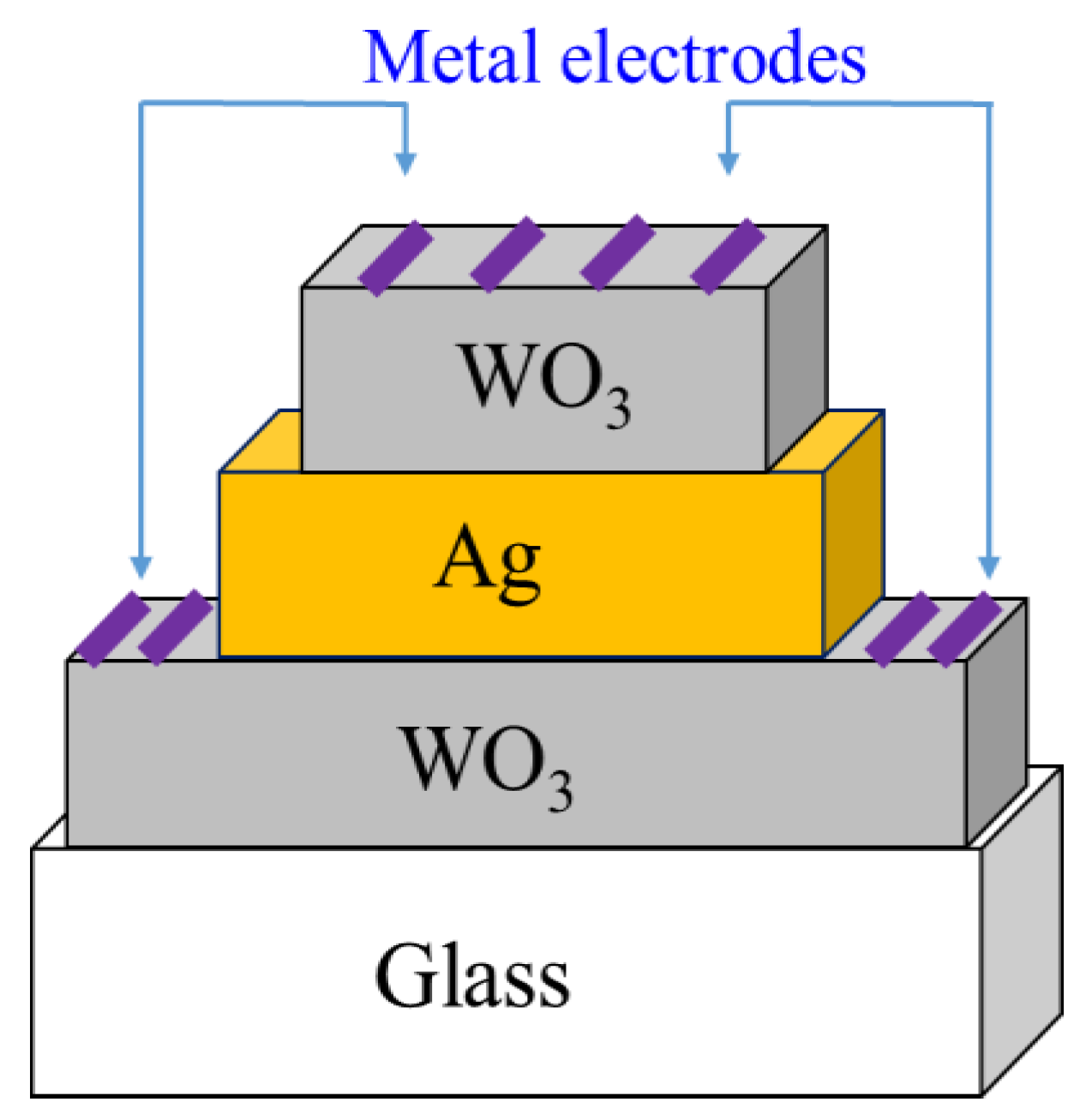
2.2. WAW Film Coated with Metal Electrodes

In order to probe how adding electrodes influences the electrical characteristics of WAW films, the metal electrodes providing the different work functions, as shown in Table 2 [15,16,17], were deposited and patterned as a comparison group. In this formation of WAW films, except for the metal sputtering as electrodes, the sputtering method was the same as above and the changing thicknesses of the silver (10 or 20 nm) and the tungsten oxide (50 or 60 nm) were also the same. After that, a layer of heat-resistant tape was also applied to the WAW film to control the deposition area to form the desired patterns. Furthermore, the area of the heat-resistant tape was used to control the area of each film. Consequently, pyramid WAW films with three different patterned electrodes of Au, Ag, or Cu electrodes with 10nm thickness sputtered on the tungsten oxide layer were formed, as shown in Figure 6, to provide the Kevin structures in the electrical performance, exposing the ohmic, space-charge limited (SCL), or trap-filling limited (TFL) mechanisms [18,19,20]. The areas of each metal electrode for upper and bottom tungsten-oxide films are 4 mm × 1 mm and 12.5 mm × 1 mm, respectively. The areas of each layer for WAW film are 25 mm × 12.5 mm, 15 mm × 7.5 mm, and 10 mm × 4 mm from bottom to top, respectively. The physical and electrical characteristics of this WAW film with sputtered electrodes were also measured and analyzed by using an X-ray diffraction analyzer (XRD), a field emission electron microscope (FE-SEM), and a Keithley 4200 semiconductor parameter analyzer.

3. Measurement Results and Discussion

In the measurement results, we discuss the electrical and physical performance of the WAW film stack. The optical transparency of the WAW film at wavelength = 550 nm is slightly investigated.

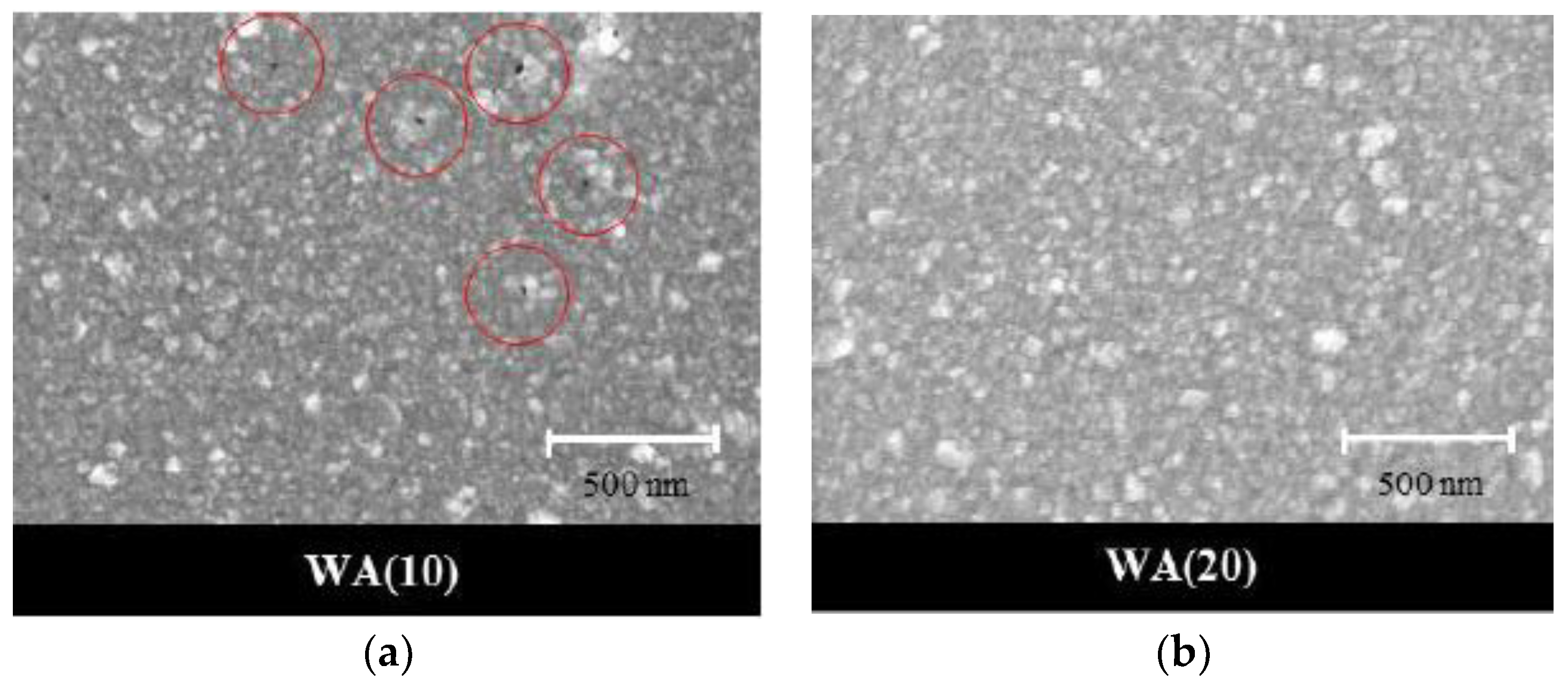
3.1. Microstructure Analysis of Silver Film Surface

First of all, the bottom WO3 with 50-nm thickness was deposited. Then, the silver (Ag) layer was sputtered up to 10 nm. During this time, the surface of this Ag film demonstrated fine black holes, which means that the Ag film was not sufficiently thick to form a continuous film. Nevertheless, as the thickness of the silver was increased up to 20 nm, the pores completely disappeared and the silver film became uniform, as shown in Figure 7.

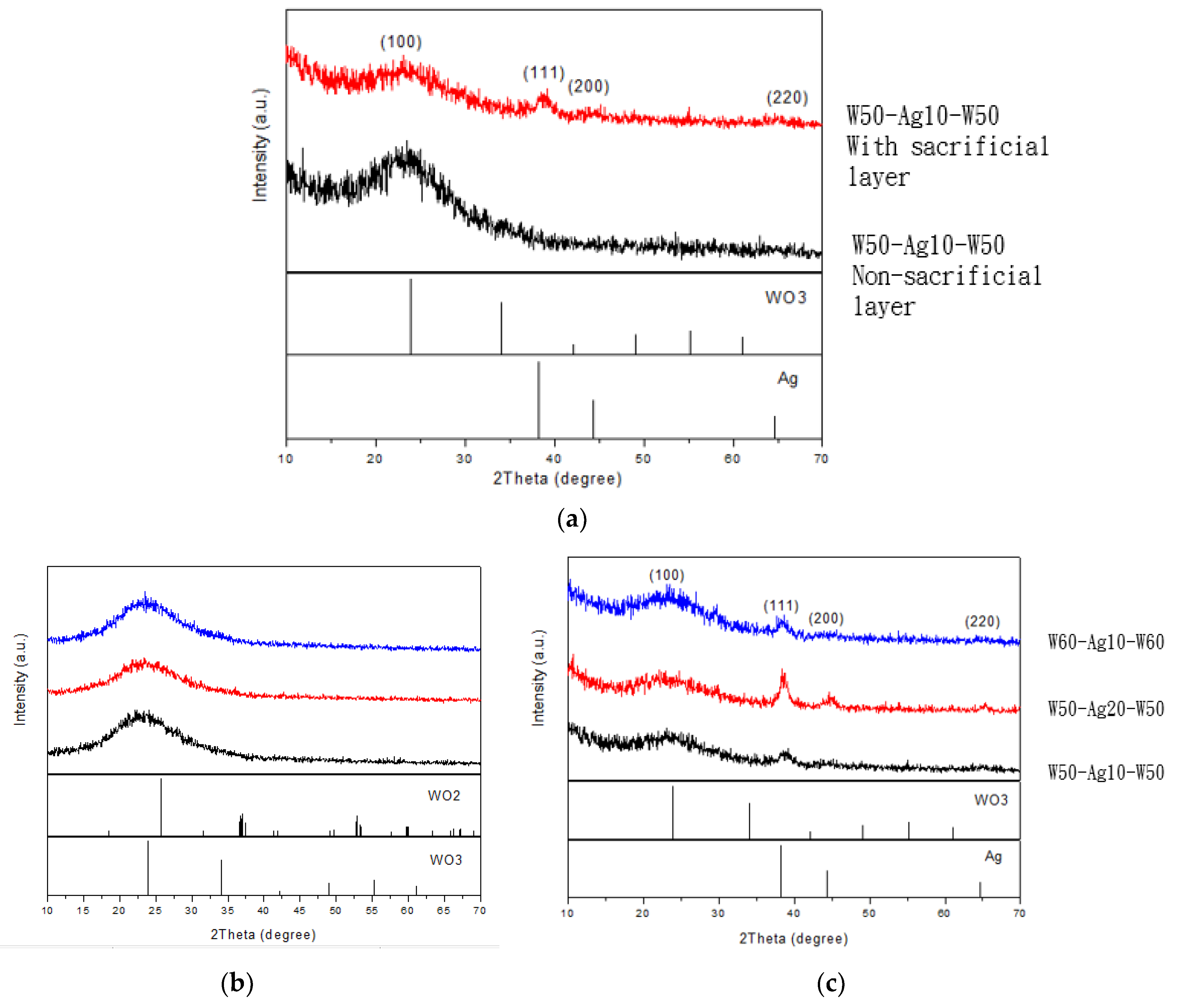
3.2. X-ray Diffraction (XRD) Analysis

As WO3/Ag/WO3 (WAW) sample was coated without a sacrificial layer W before sputtering the upper layer of tungsten oxide, the Ag film was easily oxidized as silver oxidation (AgO) decreasing the conductivity, which is not desired in applications. To prevent Ag film from the oxidation depicted in Figure 8a, a barrier layer (or called sacrificial layer) W (5-nm thickness, labeled as W5) was deposited after the formation of Ag film immediately, as shown in Figure 8b. The silver oxide [21,22,23] formed decreases the electrical conduction of the silver layer in the WAW structure and no XRD peak of silver film observed definitely represents the silver film in this un-remarkable crystallization, shown in Figure 9a. The intensity of the silver layer with XRD pattern shown in Figure 9a correlated to Figure 8b exhibits (111), (200), and (220) orientation peaks. The possible reason is that during the process of depositing the coating layer, the oxygen of the reaction gas flowing into the chamber was dissociated into oxygen ions by the plasma, and the silver was easily combined with oxygen, yet the active oxygen ions were made before the deposition of the tungsten oxide.
In the XRD pattern analysis, the WO3 (50 nm) and Ag (10 nm) films were measured separately. It can be found that the diffraction peak of tungsten oxide was not observed in Figure 9b, and the broad diffraction peak of 2θ at 20°~30° indicated that the buffer layer tungsten oxide was amorphous. Since the WO3 film formed by sputtering with the W target during sputtering, to verify whether there was oxidative unevenness, three XRD points at different locations were measured. The XRD characteristics expressed the same, and all of them were amorphous structures. In Figure 9c, in the WAW films, the thickness of the silver film was increased, and the XRD diffraction peak was apparently observed. It was found that as the thickness of the silver film increased, the intensity of the diffraction peak also increased, indicating an increment in crystallinity.

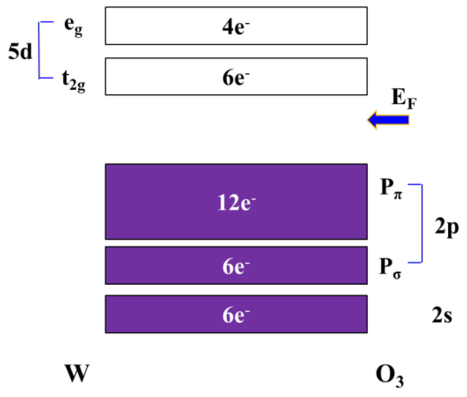
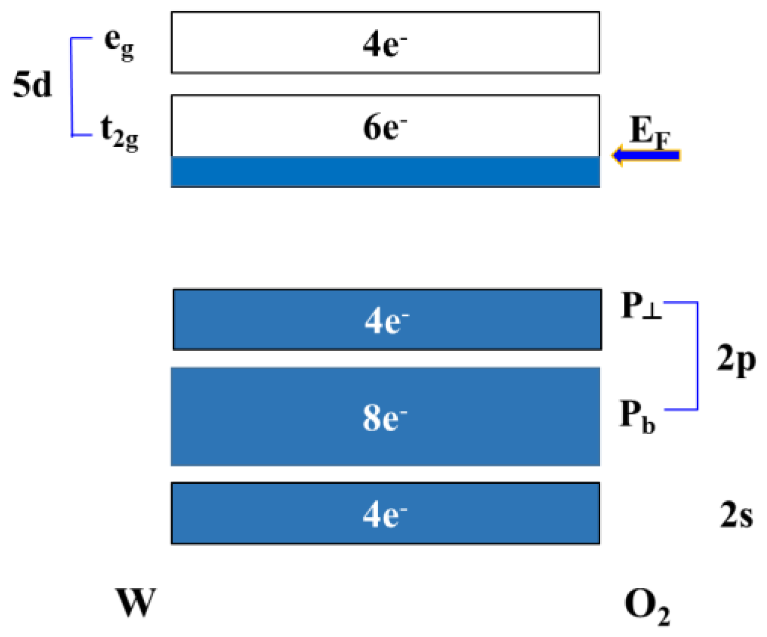
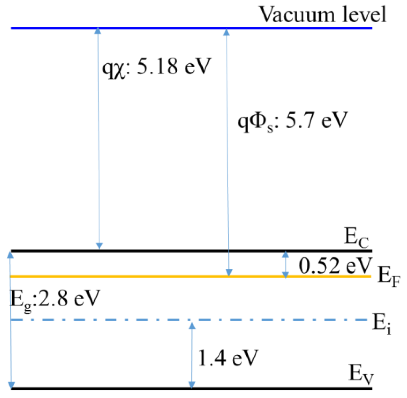
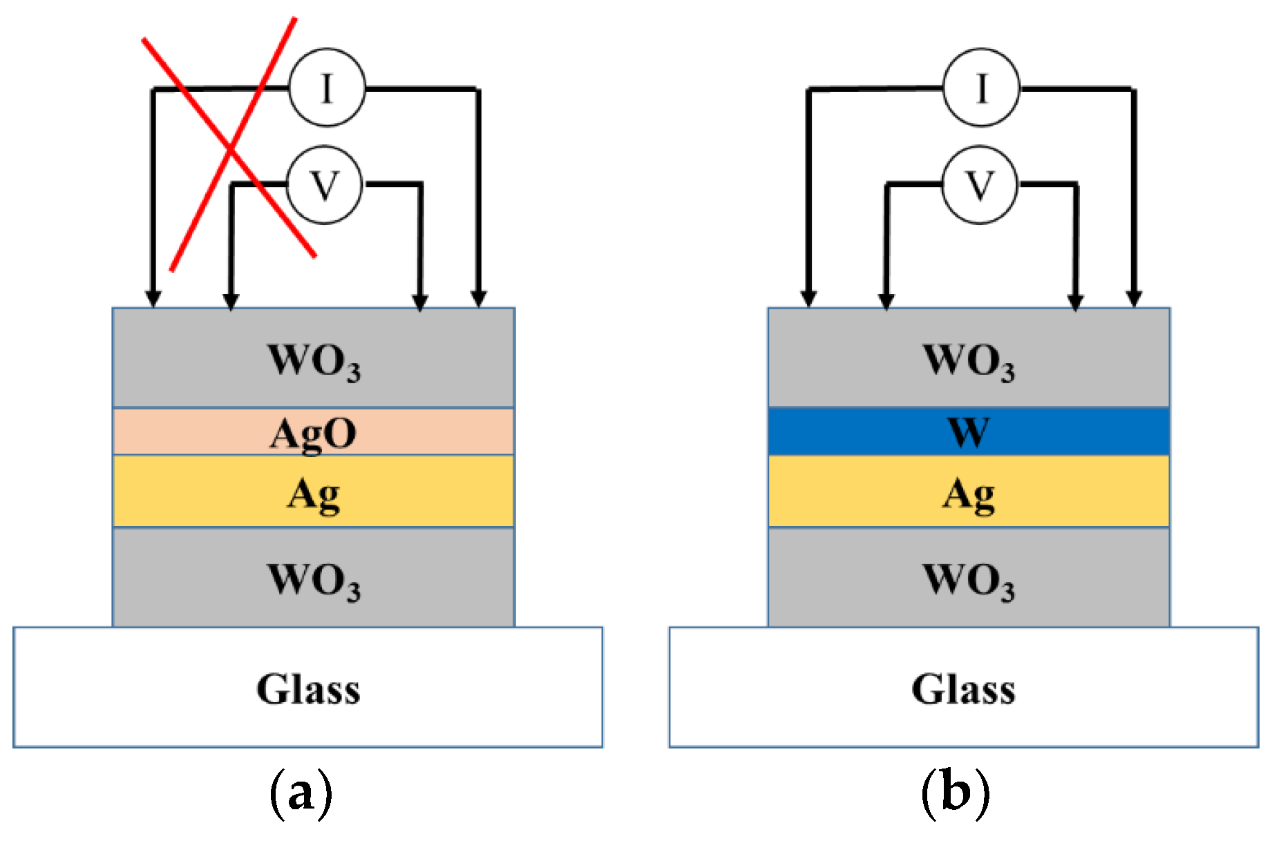
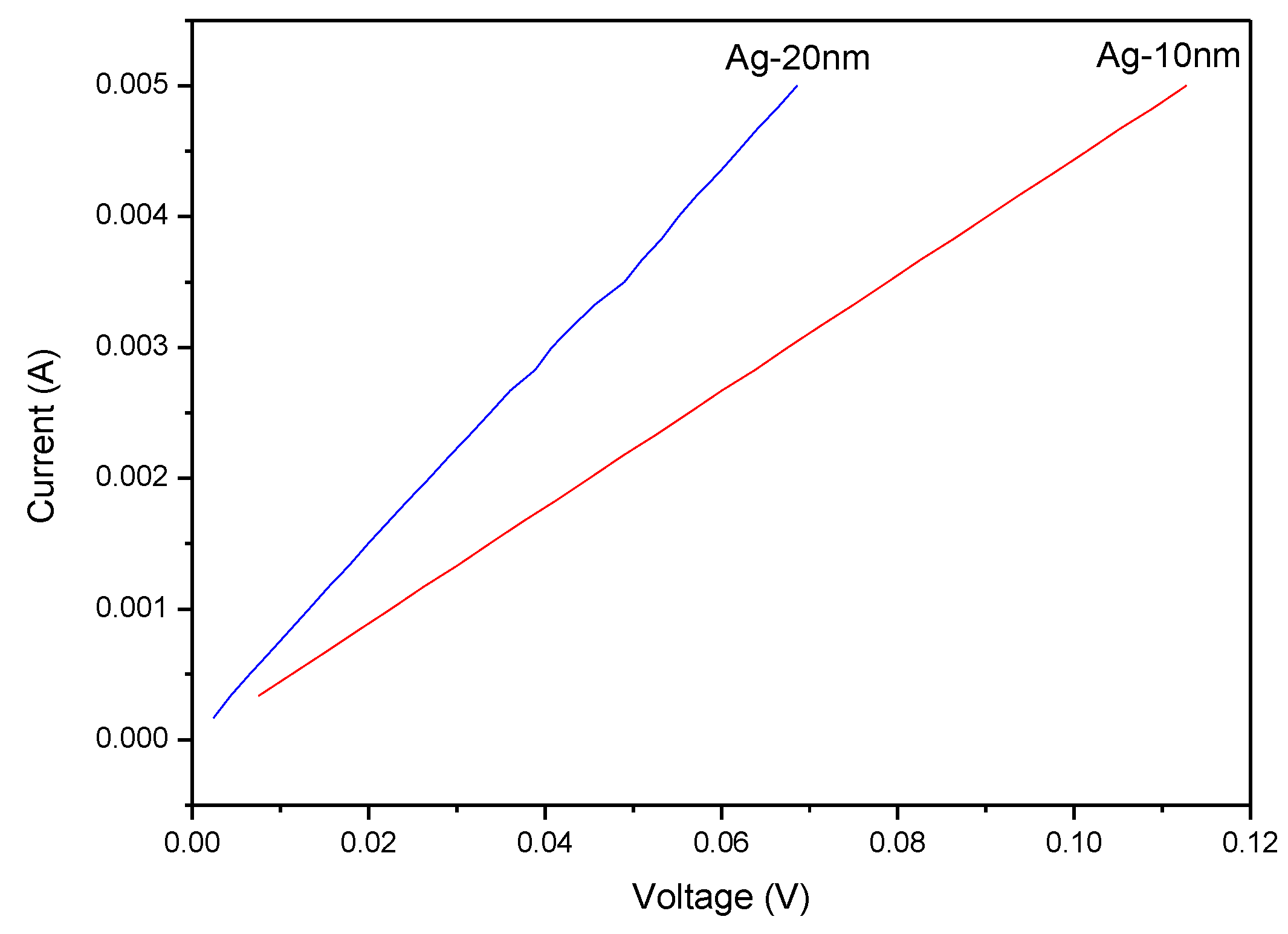
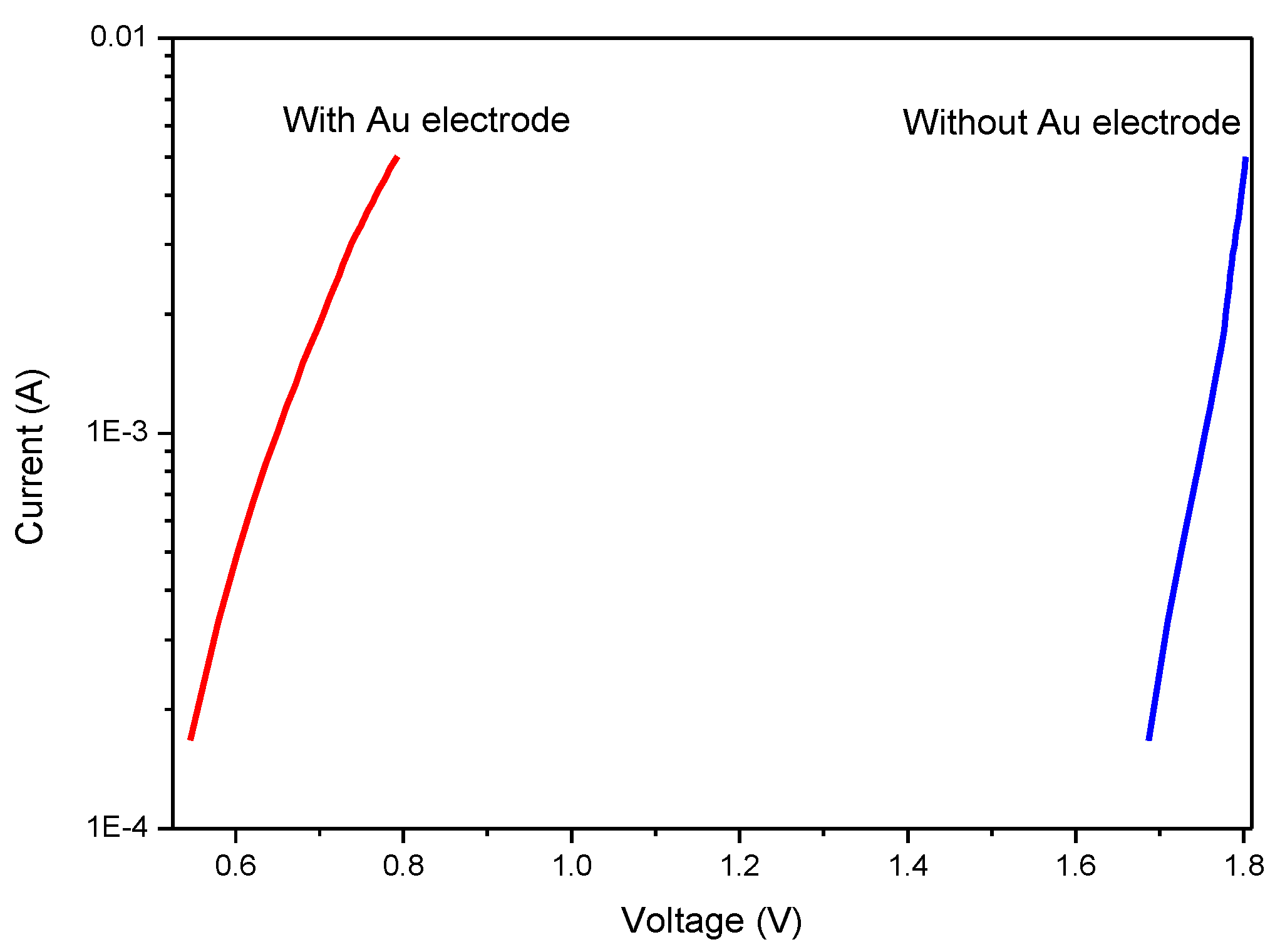
3.3. Current-Voltage Characteristics Analysis

The quality of Ag films on glass substrate, besides the observation with SEM photos in the material view, also can be evaluated with I–V characteristics, as shown in Figure 10 representing 10- and 20-nm Ag films. These two consequences are consistent and demonstrate that the thickness of Ag film increased and the resistance of that decreased.
If the WAW film is deposited with a metal electrode such as gold metal, the voltage drop at the starting voltage for a single WO3 film is tremendously improved, as shown in Figure 11. The material of the probe needle, or tungsten-titanium needle, indeed affects the electrical performance due to the probing contact resistance. While the current is fixed at 1 mA, the voltage difference between both cases is about 1.1 V from 0.65 to 1.75 V. The measurement error due to the probe contact can be reduced, which is the main benefit with the sputtering process of a gold electrode.

3.4. Light Transmittance Analysis

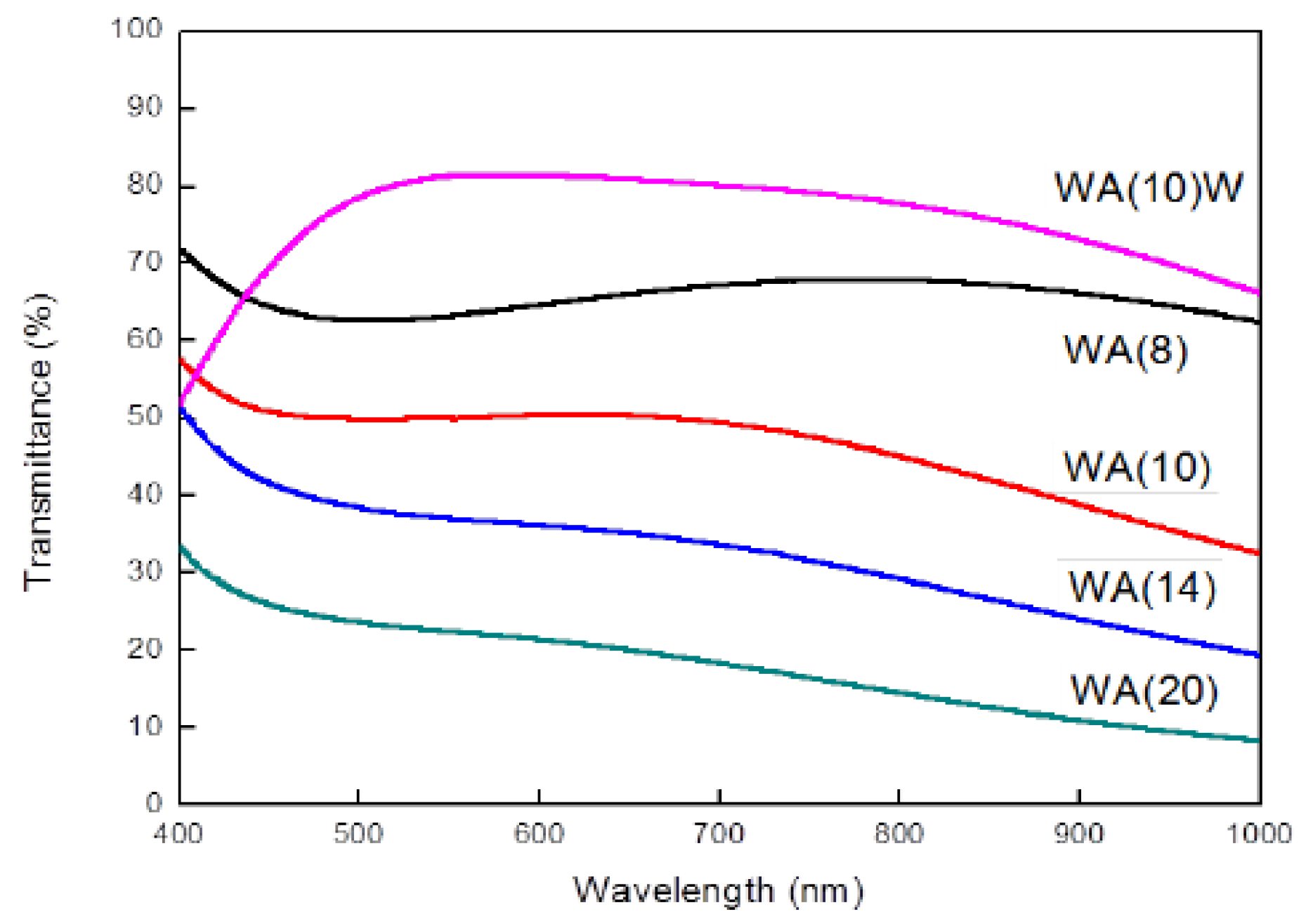
3.4.1. Optical Transmittance of WA Film

According to the UV-Vis spectrum of WA films, as shown in Figure 12, we observe that the optical transmittance (T %) [24,25] is not uniform or regular with the visible wavelengths [26]. If the top WO3 layer treated as an anti-reflective layer was deposited with 50 nm thickness, the transmittance in WA(10)W could be increased. If there were only two layers, bottom WO3 with fixed 50 nm thickness and silver layer, the thickness of the silver layer was increased and the transmittance performance was reduced. Reversely, the conductivity of the silver layer was increased according to the previous analysis. Using the wavelength = 550 nm as an example, the transmittance with the variables of silver thickness is represented at Table 3. The overall visible light transmittance at WA(8) group on average is more than 60%.

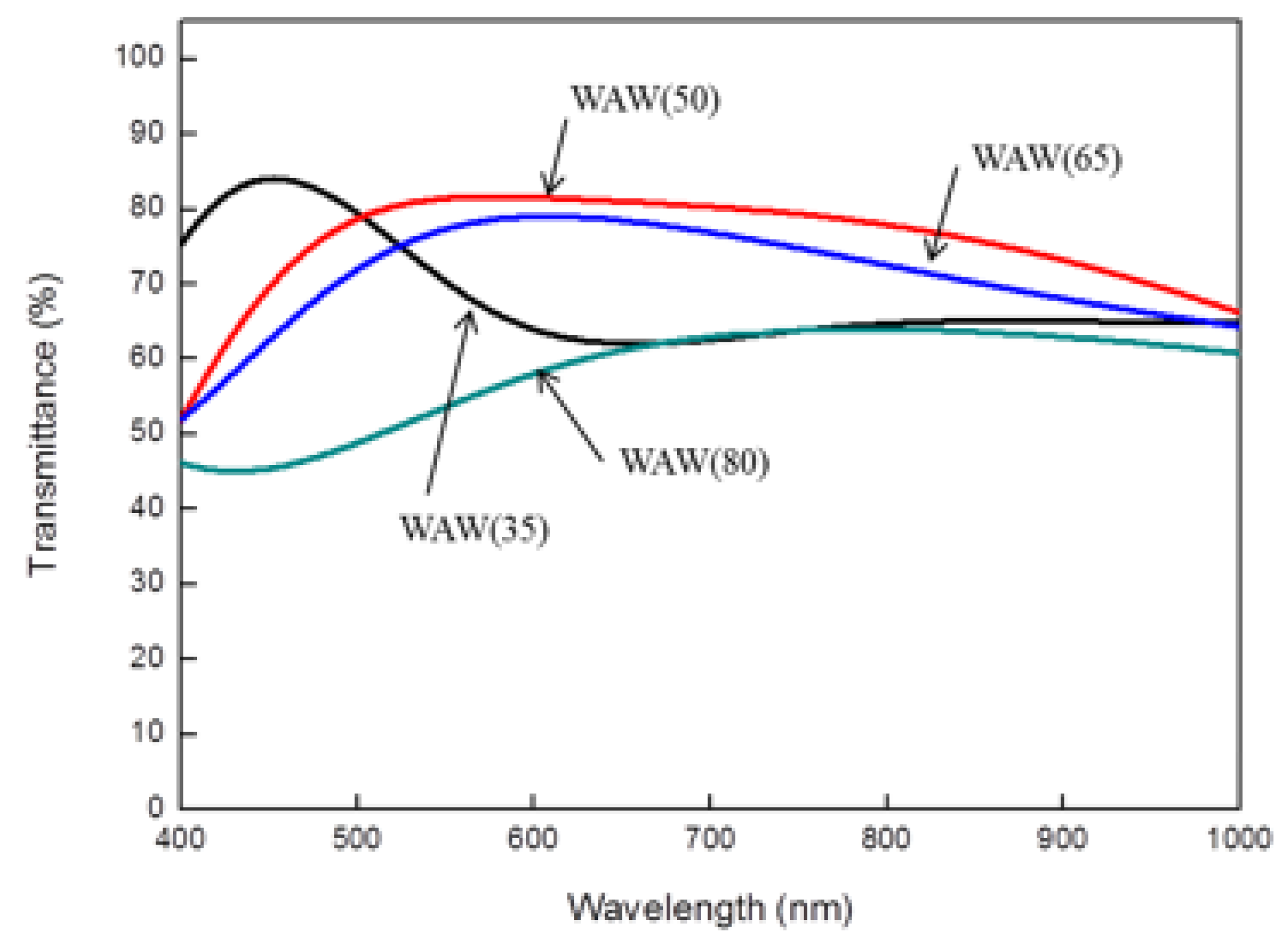
3.4.2. Optical Transmittance of WAW Film

Understanding the transmittance versus the top WO3 thicknesses as an anti-reflective layer is also important for the transparent conductive film. Following the previous section, the manufacturing process for the bottom WO3 (W(50)) and silver layers (A(10)) was identical, but the thicknesses of the top WO3 layer were changeable. The measurement results with UV-Vis spectrum are shown in Figure 13. The anti-reflectivity at the WAW(50) group is the best, which means the transmittance at = 550 nm is the maximum in these four groups, as shown Table 4 [27].

4. Conclusions

Transparent conductive films (TCF) [28] have a wide range of applications and a worldwide market. This benefit attracts the researchers to seek some feasible metrology to replace the rare metal, such as indium in ITO applications. Considering and balancing the electrical conductivity, optical transmittance, and cost effect in TCF manufacturing is zealously desired. Using a magnetron sputtering technology [29,30] different from electron beam evaporation [31] to make WAW film instead of ITO film [32] is indeed successful in this work.
Following the analysis of XRD results and SEM images to examine the crystallinity of silver film or tungsten oxide can provide a suitable growth thickness of the silver layer or tungsten oxide. With the electrical measurement and optical spectrum scanned, the optimal sputtering parameters in thickness control of the top and bottom of the tungsten oxide and silver layer can be wholly extracted and confirmed. The tunable thickness of the top tungsten oxide as an anti-reflective layer is intensely related to the transmittance. Summarizing these sensed consequences, the optimal thicknesses of WAW film should be W(50)/A(20)/W(50) in this experiment.
In this work, a thin barrier layer of tungsten on the silver film was necessarily deposited to prevent this film from oxidation and keep great conductivity for the full WAW film. In the electrical measurement, if the metal electrode is deposited, the probe resistance between the tungsten oxide and probe needle can be diminished more and the parasitic resistance confusing the measurement error also declined.

Author Contributions

Conceptualization, S.-J.W.; Formal analysis and experiment, Y.-H.L.; Funding acquisition, H.-Y.B. and C.-N.W.; Methodology, M.-C.W. and T.-S.S.; Project administration, S.-F.C.; Supervision, S.-F.C.; Writing—review & editing, M.-C.W. and Y.-H.L.

Funding

This work was supported by Ministry of Economic Affairs in Taiwan with the project number: 107-EC-17-A-22-1164.

Conflicts of Interest

The authors declare no conflict of interest.

References

  1. Wang, Z.G.; Cai, X.; Chen, Q.L.; Chu, P.K. Effects of Ti transition layer on stability of silver/titanium dioxide multilayered structure. Thin Solid Films 2007, 515, 3146–3150. [Google Scholar] [CrossRef]
  2. Wu, Z.; Chen, Z.; Du, X.; Logan, J.M.; Sippel, J.; Nikolou, M.; Kamaras, K.; Reynolds, J.R.; Tanner, D.B.; Hebard, A.F.; et al. Transparent, Conductive Carbon Nanotube Films. Science 2004, 305, 1273–1276. [Google Scholar] [CrossRef] [PubMed]
  3. Wang, C.; Chien, J.C.; Takei, K.; Takahashi, T.; Nah, J.; Niknejad, A.M.; Javey, A. Extremely bendable, high-performance integrated circuits using semiconducting carbon nanotube networks for digital, analog, and radio-frequency applications. Nano Lett. 2012, 12, 1527–1533. [Google Scholar] [CrossRef] [PubMed]
  4. Li, X.; Zhu, Y.; Cai, W.; Borysiak, M.; Han, B.; Chen, D.; Piner, R.D.; Colombo, L.; Ruoff, R.S. Transfer of large-area graphene films for high-performance transparent conductive electrodes. Nano Lett. 2009, 9, 4359–4363. [Google Scholar] [CrossRef] [PubMed]
  5. Armstronga, N.R.; Cartera, C.; Donleya, C.; Simmondsa, A.; Leea, P.; Brumbacha, M.; Kippelenb, B.; Domercqb, B.; Yoob, S. Interface modification of ITO thin films: Organic photovoltaic cells. Thin Solid Films 2003, 445, 342–352. [Google Scholar] [CrossRef]
  6. Chen, C.H.; Tseng, M.C.; Chen, Y.J.; Wuu, D.S.; Horng, R.H. Performance comparisons of light- emitting thyristors with and without indium tin oxide transparent conductive layers. Phys. Status Solidi A 2018, 215, 1700442. [Google Scholar] [CrossRef]
  7. Mergel, D.; Qiao, Z. Dielectric modelling of optical spectra of thin In2O3:Sn films. J. Phys. D Appl. Phys. 2002, 35, 794–801. [Google Scholar] [CrossRef]
  8. Badeker, K. Electrical conductivity and thermo-electromotive force of some metallic compounds. Ann. Phys. 1907, 2, 749. [Google Scholar]
  9. Yamamoto, N.; Morisawa, K.; Murakami, J.; Nakatani, Y. Formation of ITO nanowires using conventional magnetron sputtering. ESC Solid State Lett. 2014, 3, 84–86. [Google Scholar] [CrossRef]
  10. Tran, D.P.; Lu, H.I.; Lin, C.K. Conductive characteristics of indium tin oxide thin film on polymeric substrate under long-term static deformation. Coatings 2018, 8, 212. [Google Scholar] [CrossRef]
  11. Bivour, M.; Temmler, J.; Steinkemper, H.; Hermle, M. Molybdenum and tungsten oxide: High work function wide band gap contact materials for hole selective contacts of silicon solar cells. Sol. Energy Mater. Sol. Cells 2015, 142, 34–41. [Google Scholar] [CrossRef]
  12. Zhang, N.; Hu, Y.; Liu, X. Transparent organic thin film transistors with WO3/Ag/WO3 source-drain electrodes fabricated by thermal evaporation. Appl. Phys. Lett. 2013, 103, 033301. [Google Scholar] [CrossRef]
  13. Niu, W.; Bi, X.G.; Sun, X.D. Research on electrochromic mechanism of WO3 thin film. In Proceedings of the 7th National Conference on Functional Materials and Applications 2010, Hunan, China, 15–18 October 2010; ISBN 978-1-935068-41-9. [Google Scholar]
  14. Niklasson, G.A.; Granqvist, C.G. Electrochromics for smart windows: Thin films of tungsten oxide and nickel oxide, and devices based on these. J. Mater. Chem. 2007, 17, 127–156. [Google Scholar] [CrossRef]
  15. Sze, S.M. Semiconductor Device Physics and Technology, 2nd ed.; John Wiley & Sons: Hoboken, NJ, USA, 2002. [Google Scholar]
  16. Streetman, B.G.; Banerjee, S.K. Solid State Electronic Devices, 7th ed.; Pearson: New York, NY, USA, 2016. [Google Scholar]
  17. Vida, G.; Josepovits, V.K.; Gyõr, M.; Deák, P. Characterization of tungsten surfaces by simultaneous work function and secondary electron emission measurements. Microsc. Microanal. 2003, 9, 337–342. [Google Scholar] [CrossRef] [PubMed]
  18. Moliton, A.; Rammal, W.; Lucas, B. A new method for the determination of electronic mobility in organic materials. Europhys. Lett. 2005, 72, 754–759. [Google Scholar] [CrossRef]
  19. Chiu, F.C. A review on conduction mechanisms in dielectric films. Adv. Mater. Sci. Eng. 2014, 2014, 578168. [Google Scholar] [CrossRef]
  20. Sumets, M. Charge transport in LiNbO3-based heterostructures. J. Nonlinear Opt. Phys. Mater. 2017, 26, 1750011. [Google Scholar] [CrossRef]
  21. Blanc, P.; Legendre, O.; Gaucher, E.C. Estimate of clay minerals amounts from XRD pattern modeling: The Arquant model. Phys. Chem. Earth Parts A/B/C 2007, 32, 135–144. [Google Scholar] [CrossRef]
  22. Huang, T.C.; Toney, M.F.; Brennan, S.; Rek, Z. Analysis of cobalt-doped iron oxide thin films by synchrotron radiation. Thin Solid Films 1987, 154, 439–445. [Google Scholar] [CrossRef]
  23. Cullity, B.D. Elements of X-ray Diffraction, 3rd ed.; Pearson: New York, NY, USA, 2014. [Google Scholar]
  24. Granqvist, C.G. Transparent conductors as solar energy materials: A panoramic review. Sol. Energy Mater. Sol. Cells 2007, 91, 1529–1598. [Google Scholar] [CrossRef]
  25. Yanga, T.; Zhang, Z.; Song, S.; Li, Y.; Lv, M.S.; Wu, Z.; Han, S. Structural, optical and electrical properties of AZO/Cu/AZO tri-layer films prepared by radio frequency magnetron sputtering and ion-beam sputtering. Vacuum 2008, 83, 257–260. [Google Scholar] [CrossRef]
  26. Sun, S.; Wang, W.; Zeng, S.; Shang, M.; Zhang, L. Preparation of ordered mesoporous Ag/WO3 and its highly efficient degradation of acetaldehyde under visible-light irradiation. J. Hazard. Mater. 2010, 178, 427–433. [Google Scholar] [CrossRef] [PubMed]
  27. Huang, J.Y. The Study of Electrochromic Device Using WO3/Ag/WO3 Transparent Conductive Thin Films Fabricated by Magnetron Sputtering. Master’s Thesis, Department of Materials and Resources Engineering, National Taipei University of Technology, Taipei, Taiwan, 2017. [Google Scholar]
  28. Chopra, K.L.; Major, S.; Pandya, D.K. Transparent conductors-A status review. Thin Solid Films 1983, 102, 1–46. [Google Scholar] [CrossRef]
  29. Fang, G.; Li, D.; Yao, B.L. Magnetron sputtered AZO thin films on commercial ITO glass for application of a very low resistance transparent electrode. J. Phys. D Appl. Phys. 2002, 35, 3096–3100. [Google Scholar] [CrossRef]
  30. Mickan, M.; Helmersson, U.; Rinnert, H.; Ghanbaja, J.; Muller, D. Room temperature deposition of homogeneous, highly transparent and conductive Al-doped ZnO films by reactive high power impulse magnetron sputtering. Sol. Energy Mater. Sol. Cells 2016, 157, 742–749. [Google Scholar] [CrossRef]
  31. Chiu, P.K.; Cho, W.H.; Chen, H.P.; Hsiao, C.N.; Yang, J.R. Study of a sandwich structure of transparent conducting oxide films prepared by electron beam evaporation at room temperature. Nanoscale Res. Lett. 2012, 7, 304. [Google Scholar] [CrossRef] [PubMed] [Green Version]
  32. Meyer, J.; Görrn, P.; Hamwi, S.; Johannes, H.-H.; Riedl, T.; Kowalsky, W. Indium-free transparent organic light emitting diodes with Al doped ZnO electrodes grown by atomic layer and pulsed laser deposition. Appl. Phys. Lett. 2008, 93, 073308. [Google Scholar] [CrossRef]
Figure 1. Simple sketch of band diagram of WO3, where EF: Fermi level in the location. Filled energy states are colored.
Sensors 18 02803 g001
Figure 2. Schematic band profile of WO2, where EF: Fermi level in the location. Filled energy states are colored.
Sensors 18 02803 g002
Figure 3. Three-layer transparent conductive film structure of WO3/Ag/WO3 without metal electrodes.
Sensors 18 02803 g003
Figure 4. Schematic chart of process flow to fabricate a WAW film without (w/o) or with (w/) gold electrodes.
Sensors 18 02803 g004
Figure 5. Schematic diagram of band diagram of WO3 film as an n-type semiconductor.
Sensors 18 02803 g005
Figure 6. Three-layer transparent conductive film structure of WO3/Ag/WO3 with deposited metal electrodes.
Sensors 18 02803 g006
Figure 7. Scanning electron microscope (SEM) images of WA films at (a) 10-nm Ag (A10) film and (b) 20-nm Ag (A20) film.
Sensors 18 02803 g007
Figure 8. Schematic diagram of plating: (a) without barrier layer W on Ag film and (b) with W layer on Ag film.
Sensors 18 02803 g008
Figure 9. X-ray diffraction (XRD) patterns: (a) the WAW (W50: W50 nm/Ag10: Ag10 nm/W50: W50 nm) film with or without a sacrificial layer; (b) WO3 (50nm) film sensed with three locations; and (c) different film thicknesses of WAW films.
Sensors 18 02803 g009
Figure 10. Current-voltage characteristics of single-layer Ag film.
Sensors 18 02803 g010
Figure 11. I–V curves of single layer WO3 with or without gold electrode.
Sensors 18 02803 g011
Figure 12. UV-Vis spectrum of WA film at different silver thicknesses as the bottom WO3 thickness fixed.
Sensors 18 02803 g012
Figure 13. UV-Vis spectrum of WAW films at different top-WO3 thicknesses.
Sensors 18 02803 g013
Table 1. Changeable sputtering parameters in this work.
Sputtering MethodSputtering Power (W)Thickness of Tungsten Oxide (nm)Thickness of Silver Layer (nm)
RF type10050 or 6010 or 20
Table 2. Work functions (Φm) for several useful metals.
Metal SpeciesAuAgCuW
Work function (Φm, V)4.84.264.654.55
Table 3. Light transmittance of WA film under various silver thicknesses.
SampleWA (8 nm)WA (10 nm)WA (14 nm)WA (20 nm)WA (10 nm)W
T % at = 550 nm63.28%50.06%37.09%22.49%81.34%
Table 4. Light transmittance of WAW films at different top-WO3 thicknesses.
SampleWAW(35)WAW(50)WAW(65)WAW(80)
T % at = 550 nm70.37%81.34%77.28%53.58%

