Experiments on Temperature Changes of Microbolometer under Blackbody Radiation and Predictions Using Thermal Modeling by COMSOL Multiphysics Simulator

Abstract
:1. Introduction
2. Physical Structure and Optoelectronic Parameters of Microbolometer
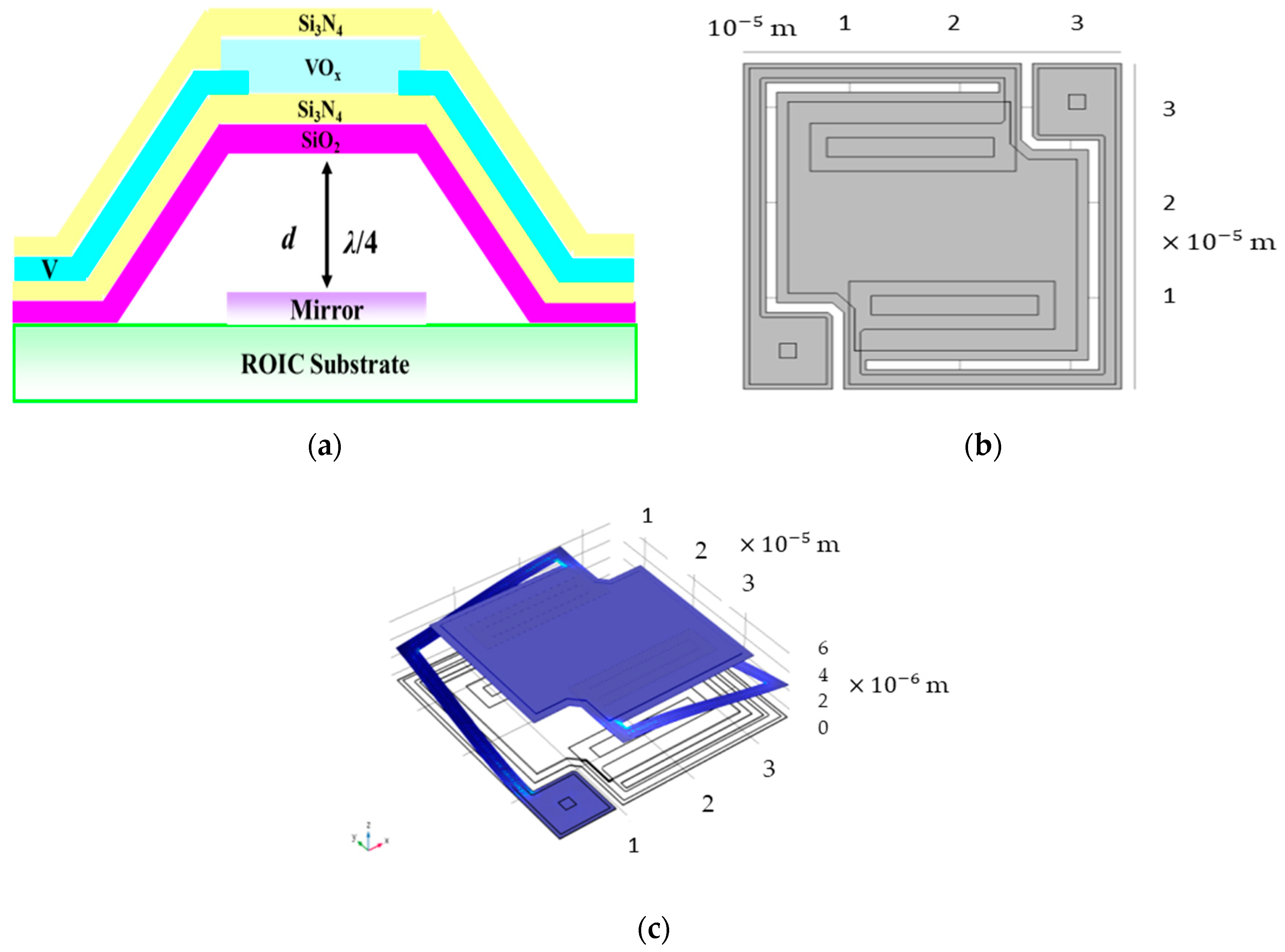
2.1. Schematics of Microbolometer Structure
2.2. Thermal Characteristics and Optoelectronic Parameters of Microbolometer
3. Microbolometer Modeling and Experimental Setup
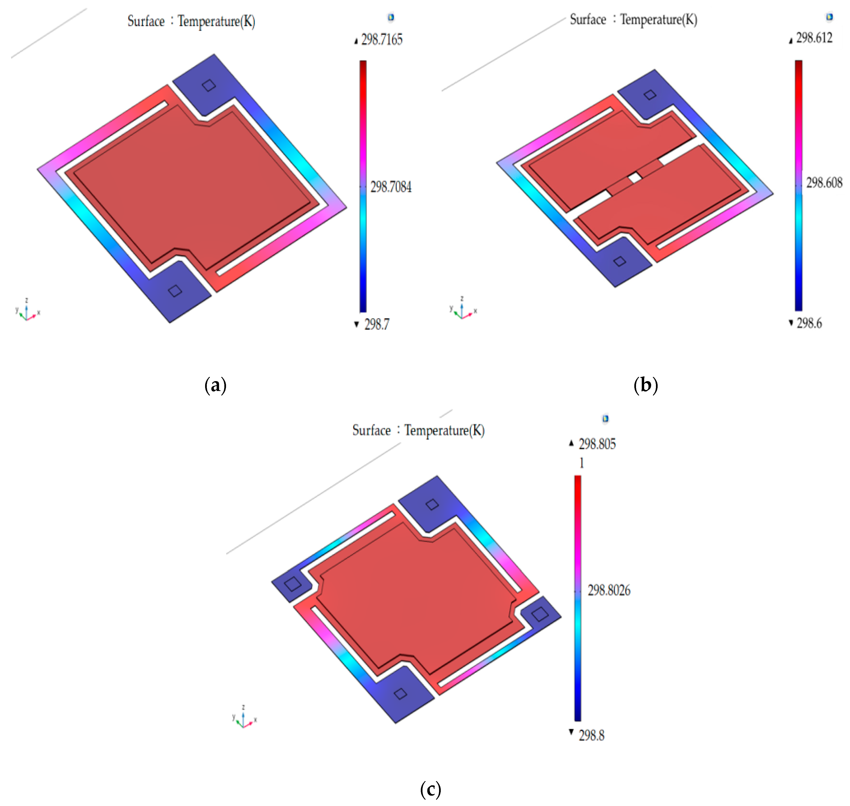
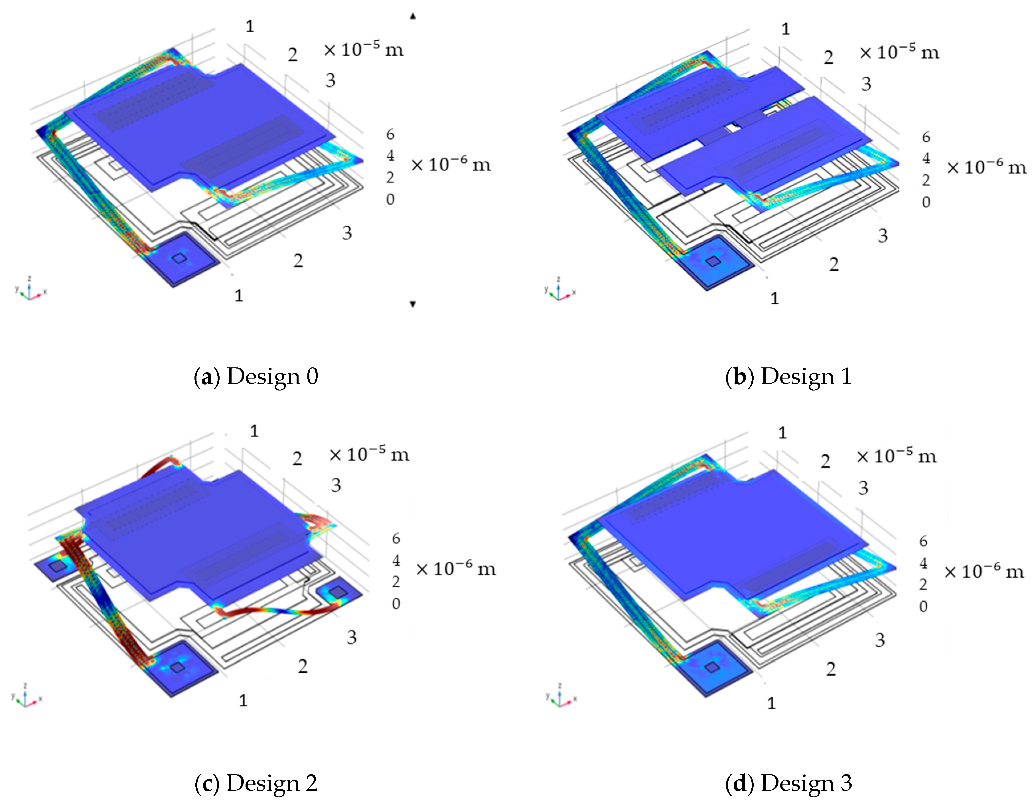
3.1. Device Structures with 4 Kinds of 35 μm-Pixel Pitch
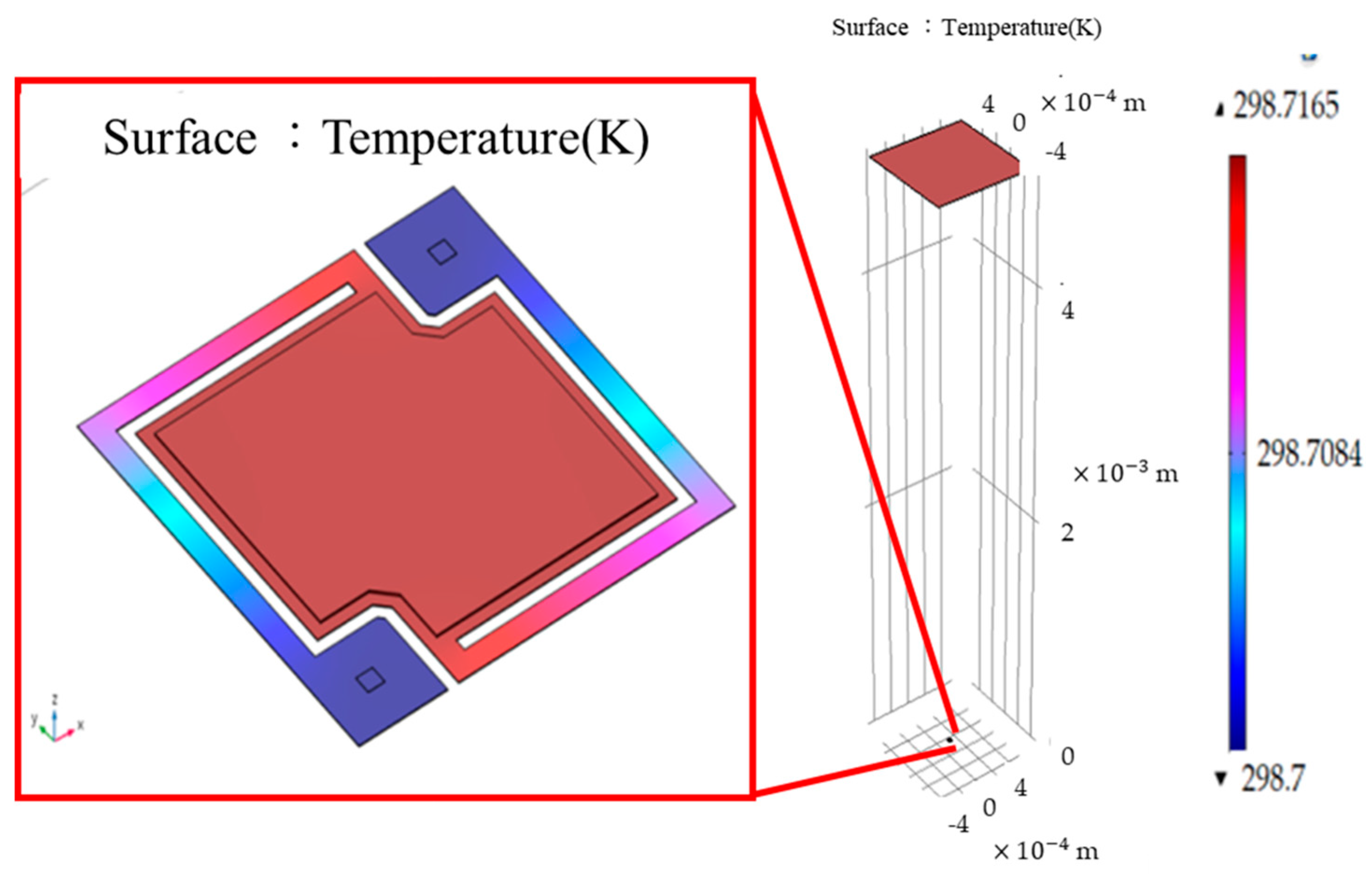
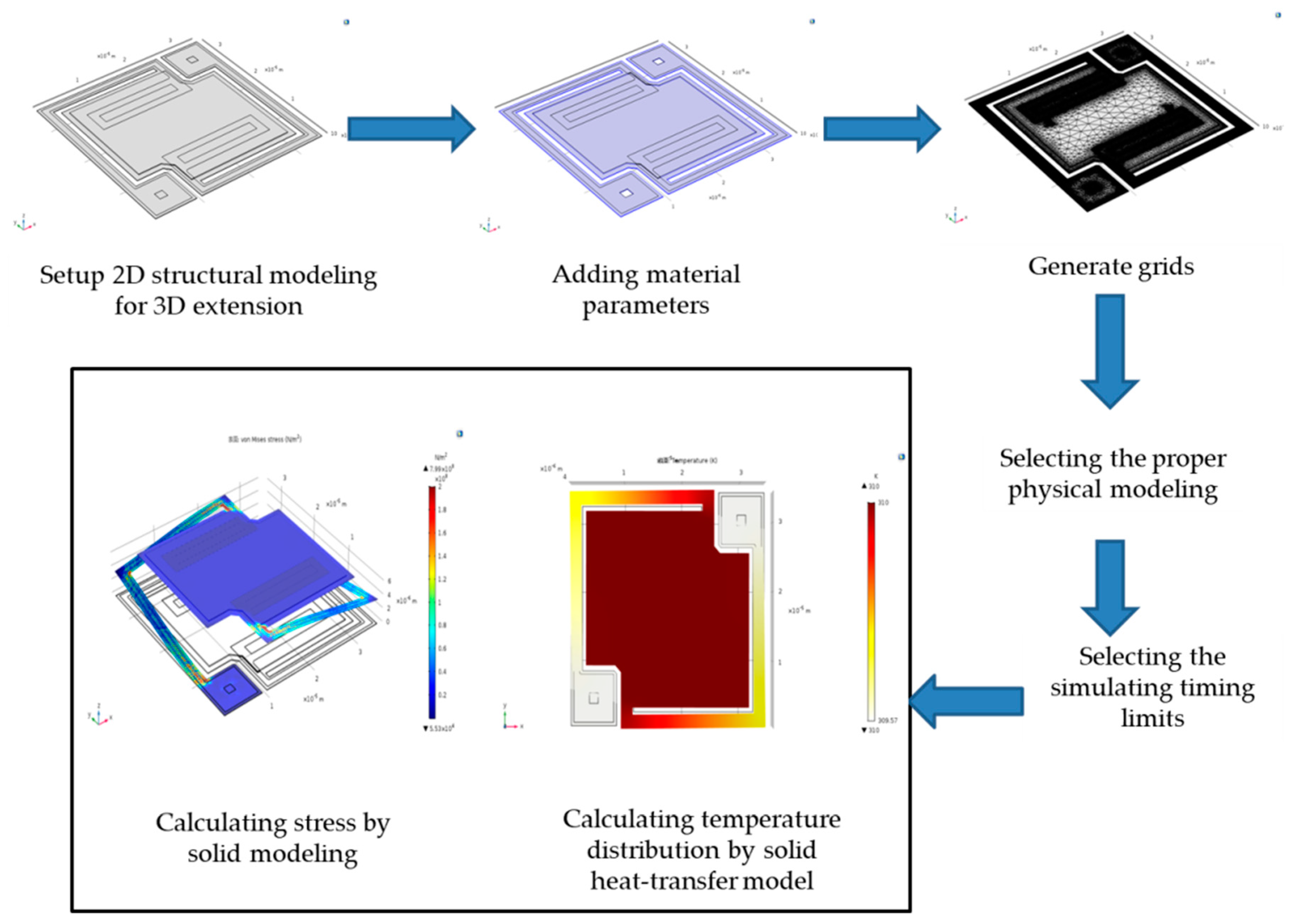
3.2. Thermal Modeling Process on 4 Kinds-of the Microbolometer Structures
- 2D geometrical structure modeling for 3D extension with the suspended device structure.
- Adding the materials of bolometer structure involved such as SiO2, Si3N4, vanadium oxide and vanadium metal.
- Using finite element method to generate the grids for the solving the optimal 3D material stress distributions in the proposed bolometer based on suspended structure efficiently.
- For simplifying the calculating complexity, the analytic modeling is introduced using geometric elastic stress under timing-imitated mode.
- Sequentially calculating the temperature distribution on the surface of suspended structure by solid heat-transfer model under illuminated from flat-plate typed black-body radiation and vacuum condition.
- Finally, the 3D stress and structure temperature distributions would be solved to be made for the performance optimization of single bolometer pixel independently.
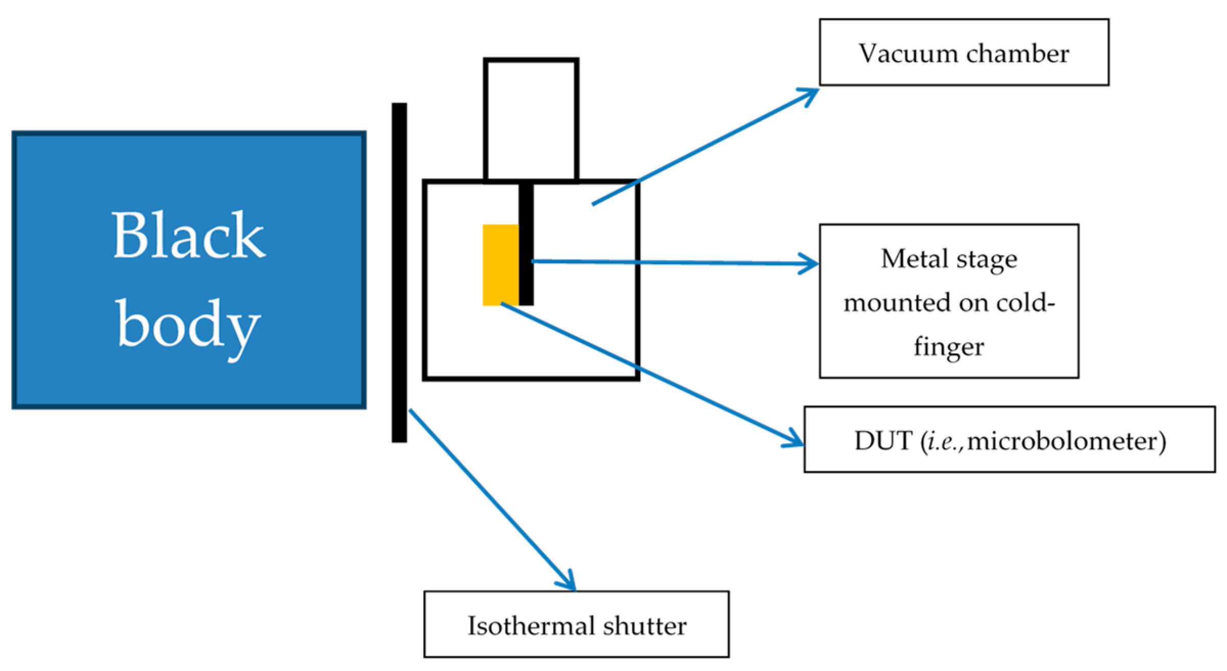
3.3. The Experimental Setup for Thermal Radiated Microbolometer Illuminated under Blackbody and Vacuum Condition
- Put the device under test (DUT) on the stage mounted on cold-finger under vacuum chamber with pumping.
- Setup the blackbody temperature of 323 K illuminated or blocked with isothermal shutter.
- Using high precise semiconductor analyzer (HP 4156 B, Agilent Technologies, Englewood, CO, USA) with sampling mode to provide the constant current of 1 μA on the DUT, the voltage signals are measured. Because treated with small direct current (DC), the self-heating of DUT could be ignored.
- During the full measured period of 90 seconds the isothermal shutter in former 30 seconds is blocked in front of DUT, later opening the isothermal shutter and blackbody source illuminating into DUT for 30 seconds, finally blocking the radiated source of blackbody for 30 seconds.
- Based on above process, the measured steps are the same for the 4 proposed DUTs and the ΔR might be extracted under the temperature of 323 K from blackbody radiation.
- Finally, the 3D stress and structure temperature distributions would be solved to be made for the performance optimization of single bolometer pixel independently.
4. Results and Discussions
5. Conclusions
Author Contributions
Funding
Conflicts of Interest
References
- Shuyu, L. Uncooled infrared focal plane array imaging in China. In Proceedings of the Conference on Infrared Technology and Applications XLI, Baltimore, MD, USA, 20–24 April 2015. [Google Scholar]
- Béland, A.; Spisser, H.; Dufour, D.; Loïc, L.N.; Francis, P.; Patrice, T. Portable LWIR hyperspectral imager based on MEMS Fabry-Perot interferometer and broadband microbolometric detector array. In Proceedings of the Conference on MOEMS and Miniaturized Systems XVII, San Francisco, CA, USA, 27 January–1 February 2018. [Google Scholar]
- Masafumi, K. Uncooled infrared focal plane arrays. IEEE Trans. Electr. Electron. Eng. 2018, 13, 4–12. [Google Scholar]
- Kruse, P.W.; Skatrud, D.D. Uncooled Infrared Imaging Arrays and Systems; Academic Press: Cambridge, MA, USA, 1997. [Google Scholar]
- Zeng, H.Y.; Tang, S.F.; Chen, T.C. Performance evaluation for uncooled microbolometer using antireflection coating of SiO2/Si3N4 multiple films on silicon window. Sens. Mater. 2018, 30, 339–345. [Google Scholar]
- Wu, Z.Y.; Tang, S.F.; Zeng, H.Y.; Lin, W.J.; Chen, T.C.; Gau, Y.T. Infrared response of vanadium oxide (VOx)/SiNx/reduced graphene oxide (rGO) composite microbolometer. Microelectron. Reliab. 2018. [Google Scholar] [CrossRef]
- Chao, C.; Zheng, X.; Zhou, Y.D. Uncooled microbolometer system level co-simulation using finite element analysis method and intellectual property core. Microsyst. Technol. 2017, 23, 2215–2222. [Google Scholar]
- Zhou, P.; Chen, R.; Wang, N.; San, H.; Chen, X. Reliability design and electro-thermal-optical simulation of bridge-Style infrared thermal emitters. Micromachines 2016, 7, 166. [Google Scholar] [CrossRef]
- Piotr, Z.; Cezary, M.; Michał, S.; Mykhaylo, L.; Andrzej, N. Analytical thermo-electric model of uncooled microbolometer. Mach. Dyn. Res. 2013, 37, 99–105. [Google Scholar]
- Thomas, J.; Crompton, J.S.; Koppenhoefer, K.C. Multiphysics analysis of Infrared Bolometer. In Proceedings of the 2015 COMSOL Conference in Boston, Boston, MA, USA, 7–9 October 2015. [Google Scholar]
- Chen, R.; Yu, T. Thermal design of CMOS uncooled infrared Sensors. Bull. Adv. Technol. Res. 2010, 4, 6–10. [Google Scholar]


| Material | Thermal Conductivity (W/cm·K) | Thermal Capacitance (J/kg·K) | Density (g/cm3) | Resistivity (Ω cm) | Young Modulus (GPa) | Poisson’s Ratio |
|---|---|---|---|---|---|---|
| SiO2 | 1.4 | 787 | 2.196 | ~1023 | 75 | 0.17 |
| Si3N4 | 0.02 | 3.33 | 2.3 | ~1015 | 300 | 0.26 |
| VOX | 0.05 | 5.00 | 4.34 | 1 | 80 | 0.24 |
| Vanadium | 3.07 | 489 | 6 | 1.97 × 10⁻⁷ | 128 | 0.37 |
| Parameter | Design 0 (D0) | Design1 (D1) | Design 2 (D2) | Design 3 (D3) |
|---|---|---|---|---|
| Number of legs | 2 | 4 | 2 | |
| Si3N4/V in each leg length (μm) | 66/60 | 33/30 | 66/60 | |
| Leg shape (μm) | L | L | I | L |
| Vacancy on platform | n/a | Center: 2 μm × 2 μm Slits: 2 μm × 7.5 μm | n/a | n/a |
| Spacing of electrodes on the platform (μm) | 14.5 | increase the space from 14.5 (standard) to 20.5 | ||
| Unit | Design 0 (D0) | Design 1 (D1) | Design 2 (D2) | Design 3 (D3) | |
|---|---|---|---|---|---|
| Response time | (mS) | 6.96 | 6.59 | 2.73 | 6.02 |
| G | W/T | 7.9827 10−10 | 7.72692 10−10 | 1.57 10−9 | 8.0516 10−10 |
| Responsivity | V/W | 6.899 104 | 1.22614 105 | 2.8306 104 | 1.25148 105 |
| Detectivity | 9.11595 108 | 1.6092 109 | 3.7369 108 | 1.64653 109 | |
| NEP | W | 3.839 10−12 | 2.1749 10−12 | 9.366 10−12 | 2.1257 10−12 |
| η% | - | 6.615 | 9.474 | 5.338 | 11.347 |
| NETD | mK | 99.219 | 39.24 | 299.962 | 32.028 |
| Design 0 (D0) | Design 1 (D1) | Design 2 (D2) | Design 3 (D3) | |
|---|---|---|---|---|
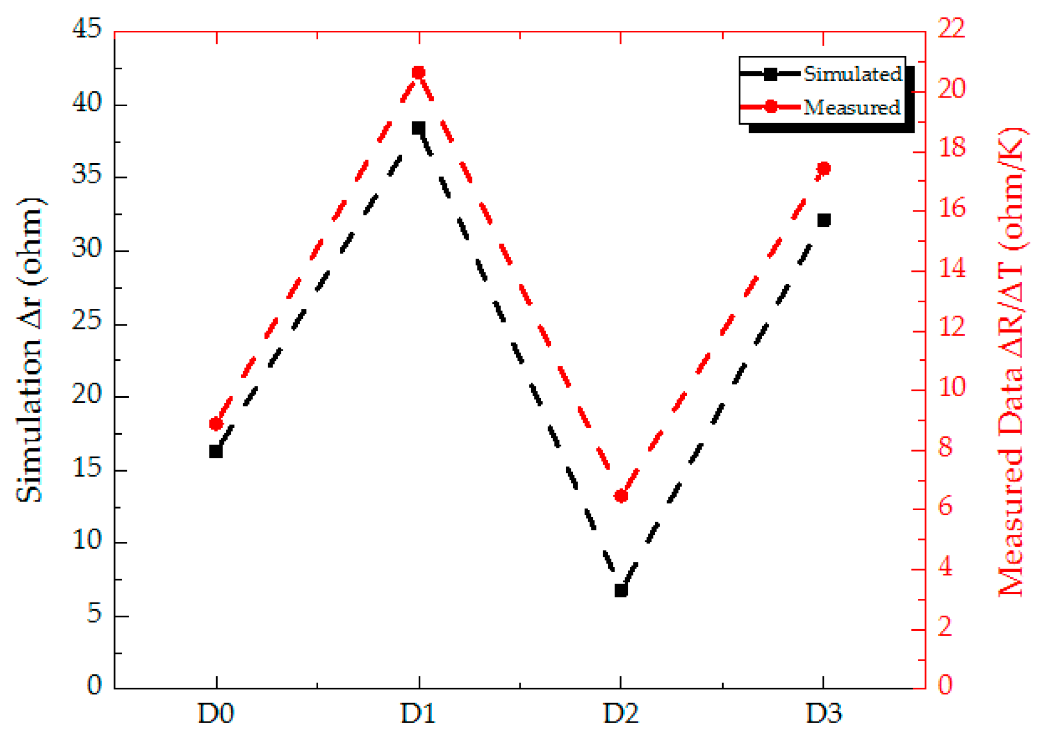
| Thermal equivalent resistance differences Δr (Ω) | 16.291 | 38.448 | 6.802 | 32.160 |
| Design 0 (D0) | Design 1 (D1) | Design 2 (D2) | Design 3 (D3) | |
|---|---|---|---|---|
| ΔV (mV) | 0.209 | 0.528 | 0.156 | 0.448 |
| ΔR/ΔT (Ω/K) | 8.886 | 20.64 | 6.475 | 17.43 |
© 2018 by the authors. Licensee MDPI, Basel, Switzerland. This article is an open access article distributed under the terms and conditions of the Creative Commons Attribution (CC BY) license (http://creativecommons.org/licenses/by/4.0/).
Share and Cite
Deng, Y.-Z.; Tang, S.-F.; Zeng, H.-Y.; Wu, Z.-Y.; Tung, D.-K. Experiments on Temperature Changes of Microbolometer under Blackbody Radiation and Predictions Using Thermal Modeling by COMSOL Multiphysics Simulator. Sensors 2018, 18, 2593. https://doi.org/10.3390/s18082593
Deng Y-Z, Tang S-F, Zeng H-Y, Wu Z-Y, Tung D-K. Experiments on Temperature Changes of Microbolometer under Blackbody Radiation and Predictions Using Thermal Modeling by COMSOL Multiphysics Simulator. Sensors. 2018; 18(8):2593. https://doi.org/10.3390/s18082593
Chicago/Turabian StyleDeng, Yu-Zhen, Shiang-Feng Tang, Hong-Yuan Zeng, Zheng-Yuan Wu, and Der-Kuo Tung. 2018. "Experiments on Temperature Changes of Microbolometer under Blackbody Radiation and Predictions Using Thermal Modeling by COMSOL Multiphysics Simulator" Sensors 18, no. 8: 2593. https://doi.org/10.3390/s18082593