One-Step Laser Patterned Highly Uniform Reduced Graphene Oxide Thin Films for Circuit-Enabled Tattoo and Flexible Humidity Sensor Application


Abstract
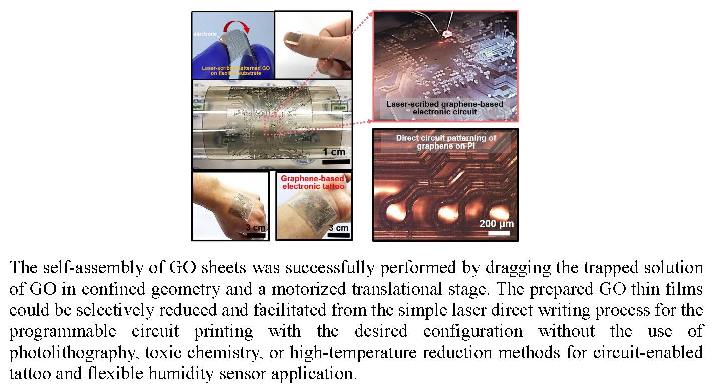
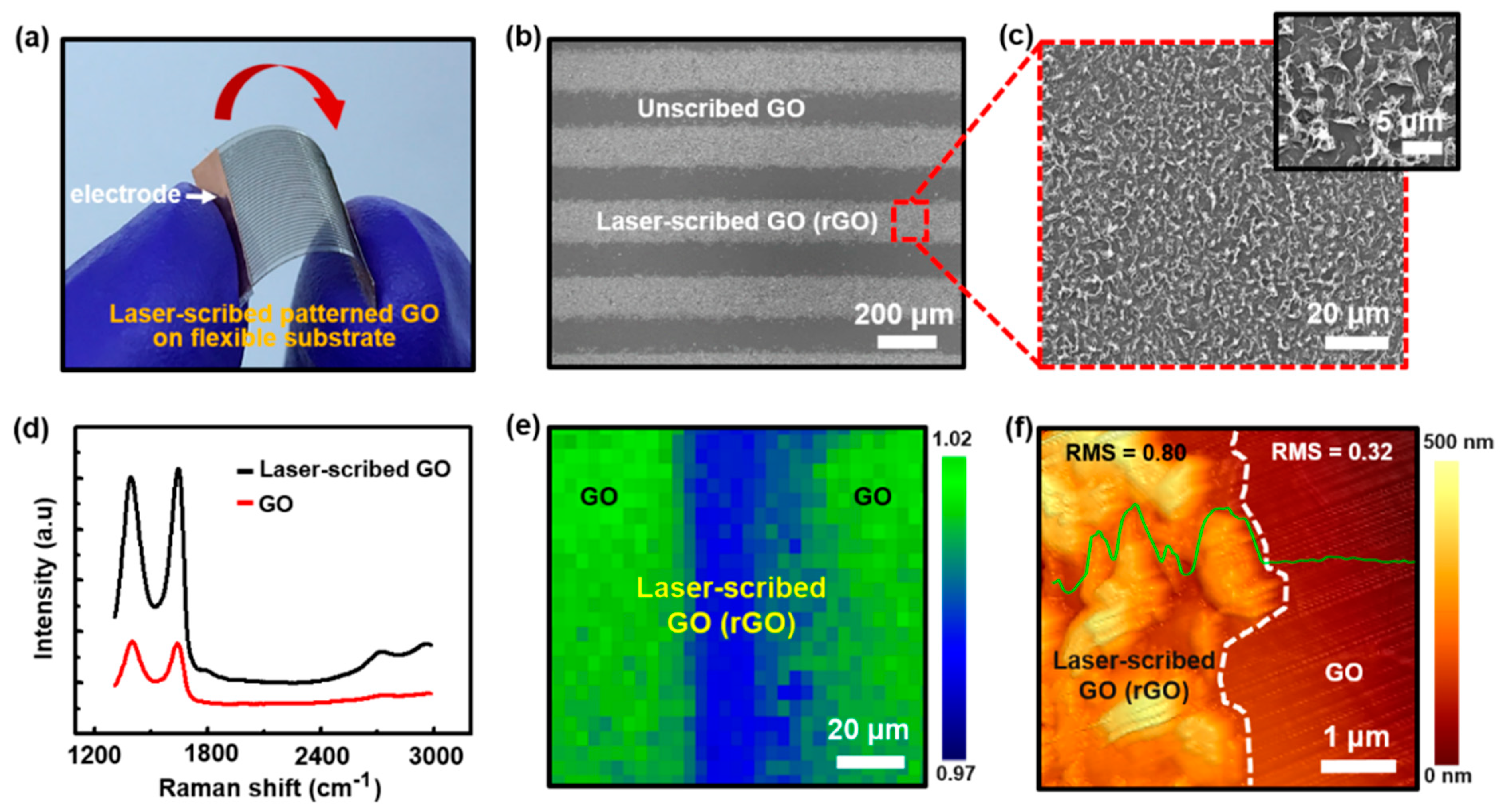
:
1. Introduction
2. Materials and Methods
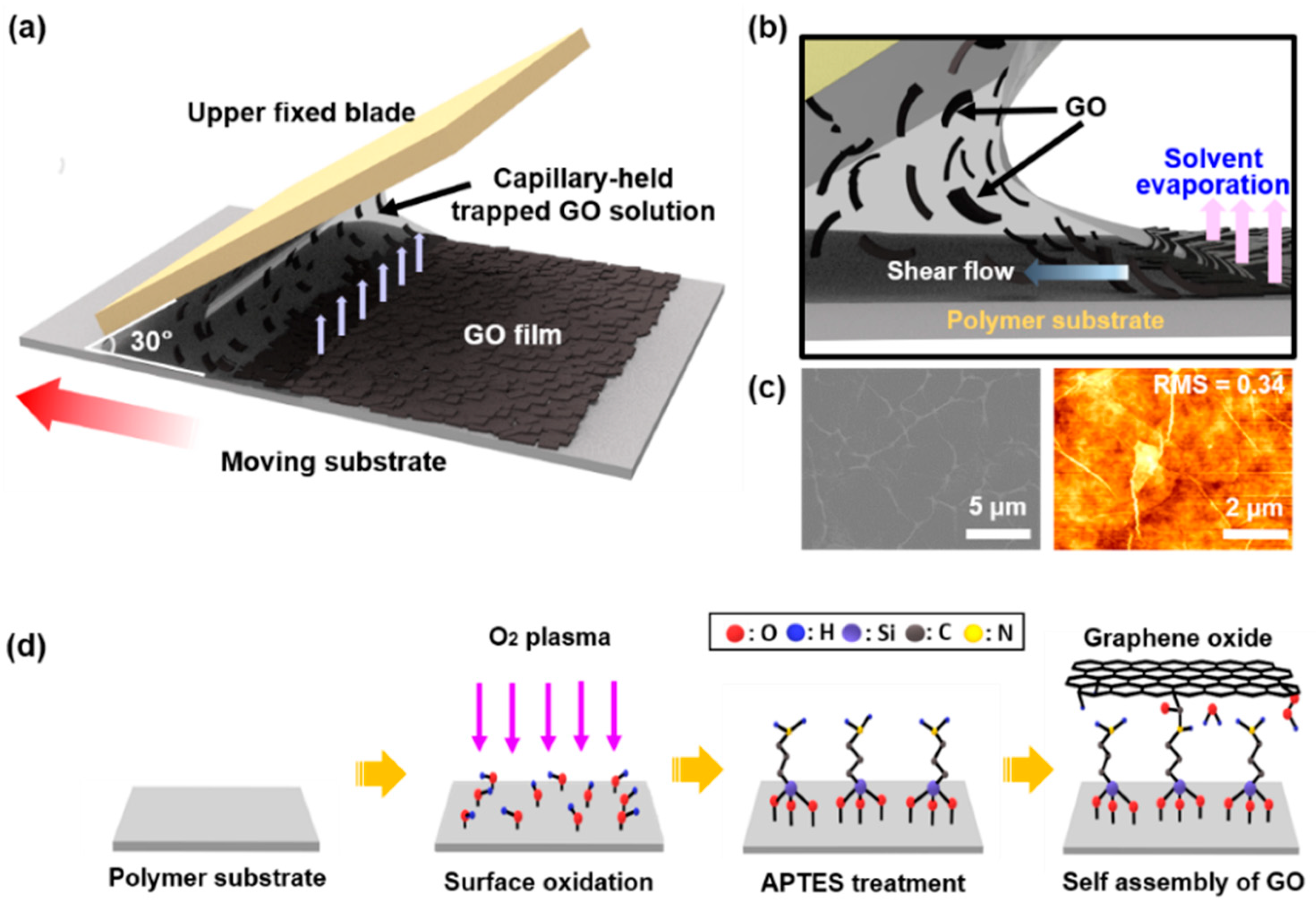
2.1. Highly Uniform Thin GO-Film Fabrication via FESA Process on Polymer Substrate
2.2. Surface Modification of PP Film and Self-Assembled APTES-GO Sheet
2.3. Characterization and Measurements
3. Results and Discussion
4. Conclusions
Supplementary Materials
Author Contributions
Funding
Conflicts of Interest
References
- Novoselov, K.S.; Geim, A.K.; Morozov, S.V.; Jiang, D.; Zhang, Y.; Dubonos, S.V.; Grigorieva, I.V.; Firsov, A.A. Electric field effect in atomically thin carbon films. Science 2004, 306, 666–669. [Google Scholar] [CrossRef] [PubMed]
- Mak, K.F.; Shan, J.; Heinz, T.F. Electronic structure of few-layer graphene: experimental demonstration of strong dependence on stacking sequence. Phys. Rev. Lett. 2010, 104, 176404. [Google Scholar] [CrossRef] [PubMed]
- Chen, J.; Duan, M.; Chen, G. Continuous mechanical exfoliation of graphene sheets via three-roll mill. J. Mater. Chem. 2012, 22, 19625–19628. [Google Scholar] [CrossRef]
- Somani, P.R.; Somani, S.P.; Umeno, M. Planer nano-graphenes from camphor by CVD. Chem. Phys. Lett. 2006, 430, 56–59. [Google Scholar] [CrossRef]
- Bo, Z.; Yang, Y.; Chen, J.; Yu, K.; Yan, J.; Cen, K. Plasma-enhanced chemical vapor deposition synthesis of vertically oriented graphene nanosheets. Nanoscale 2013, 5, 5180–5204. [Google Scholar] [CrossRef] [PubMed]
- Stankovich, S.; Dikin, D.A.; Piner, R.D.; Kohlhaas, K.A.; Kleinhammes, A.; Jia, Y.; Wu, Y.; Nguyen, S.T.; Ruoff, R.S. Synthesis of graphene-based nanosheets via chemical reduction of exfoliated graphite oxide. Carbon 2007, 45, 1558–1565. [Google Scholar] [CrossRef]
- Badami, D.V. Graphitization of α-Silicon Carbide. Nature 1962, 193, 569–570. [Google Scholar] [CrossRef]
- Zhao, W.; Fang, M.; Wu, F.; Wu, H.; Wang, L.; Chen, G. Preparation of graphene by exfoliation of graphite using wet ball milling. J. Mater. Chem. 2010, 20, 5817–5819. [Google Scholar] [CrossRef]
- Kosynkin, D.V.; Higginbotham, A.L.; Sinitskii, A.; Lomeda, J.R.; Dimiev, A.; Price, B.K.; Tour, J.M. Longitudinal unzipping of carbon nanotubes to form graphene nanoribbons. Nature 2009, 458, 872–876. [Google Scholar] [CrossRef] [PubMed] [Green Version]
- Pei, S.; Cheng, H.-M. The reduction of graphene oxide. Carbon 2012, 50, 3210–3228. [Google Scholar] [CrossRef]
- Compton, O.C.; Nguyen, S.T. Graphene oxide, highly reduced graphene oxide, and graphene: Versatile building blocks for carbon-based material. Small 2010, 5, 711–723. [Google Scholar] [CrossRef] [PubMed]
- Mao, S.; Pu, H.; Chen, J. Graphene oxide and its reduction: Modeling and experimental progress. RSC Adv. 2012, 2, 2643–2662. [Google Scholar] [CrossRef]
- Dreyer, D.R.; Park, S.; Bielawski, C.W.; Ruoff, R.S. The chemistry of graphene oxide. Chem. Soc. Rev. 2010, 39, 228–240. [Google Scholar] [CrossRef] [PubMed]
- Szabo, T.; Berkesi, O.; Forgo, P.; Josepovits, K.; Sanakis, Y.; Petridis, D.; Dekany, I. Evolution of surface functional groups in a series of progressively oxidized graphite oxides. Chem. Mater. 2006, 18, 2740–2749. [Google Scholar] [CrossRef]
- Boukhvalov, D.W.; Katsnelson, M.I. Modeling of graphite oxide. J. Am. Chem. Soc. 2008, 130, 10697–10701. [Google Scholar] [CrossRef] [PubMed]
- Chang, H.; Wang, G.; Yang, A.; Tao, X.; Liu, X.; Shen, Y.; Zheng, Z. A transparent, flexible, low-temperature, and solution-processible graphene composite electrode. Adv. Funct. Mater. 2010, 20, 2893–2902. [Google Scholar] [CrossRef]
- Eda, G.; Chhowalla, M. Graphene-based composite thin films for electronics. Nano Lett. 2009, 9, 814–818. [Google Scholar] [CrossRef] [PubMed]
- Pang, S.; Tsao, H.N.; Feng, X.; Mullen, K. Patterned graphene electrodes from solution-processed graphite oxide films for organic field-effect transistors. Adv. Mater. 2009, 21, 3488–3491. [Google Scholar] [CrossRef]
- Meric, I.; Han, M.Y.; Young, A.F.; Ozyilmaz, B.; Kim, P.; Shepard, K.L. Current saturation in zero-bandgap, top-gated graphene field-effect transistors. Nat. Nanotechnol. 2008, 3, 654–659. [Google Scholar] [CrossRef] [PubMed]
- Mohanty, N.; Berry, V. Graphene-based single-bacterium resolution biodevice and DNA transistor: Interfacing graphene derivative with nanoscale and microscale biocomponents. Nano Lett. 2008, 8, 4469–4476. [Google Scholar] [CrossRef] [PubMed]
- He, Q.; Sudibya, H.G.; Yin, Z.; Wu, S.; Li, H.; Boey, F.; Huang, W.; Chen, P.; Zhang, H. Centimeter-long and large-scale micropatterns of reduced graphene oxide films: Fabrication and sensing application. ACS Nano 2010, 4, 3201–3208. [Google Scholar] [CrossRef] [PubMed]
- Liu, Z.; Liu, Q.; Huang, Y.; Ma, Y.; Yin, S.; Zhang, X.; Sun, W.; Chen, Y. Organic photovoltaic devices based on a novel acceptor material: Graphene. Adv. Mater. 2008, 20, 3924–3930. [Google Scholar] [CrossRef]
- Yan, X.; Cui, X.; Li, B.; Li, L.S. Large, solution-processable graphene quantum dots as light absorbers for photovoltaics. Nano Lett. 2010, 10, 1869–1873. [Google Scholar] [CrossRef] [PubMed]
- Shin, K.Y.; Hong, J.Y.; Jang, J. Flexible and transparent graphene films as acoustic actuator electrodes using inkjet printing. Chem. Commun. 2011, 47, 8527–8529. [Google Scholar] [CrossRef] [PubMed]
- Liang, Q.; Yao, X.; Wang, W.; Liu, Y.; Wong, C.P. A three-dimensional vertically aligned functionalized multilayer graphene architecture: an approach for graphene-based thermal interfacial materials. ACS Nano 2011, 5, 2392–2401. [Google Scholar] [CrossRef] [PubMed]
- Zou, F.; Zhou, H.; Jeong, D.Y.; Kwon, J.; Eom, S.U.; Park, T.J.; Hong, S.W.; Lee, J. Wrinkled surface-mediated antibacterial activity of graphene oxide nanosheets. ACS Appl. Mater. Interfaces 2017, 9, 1343–1351. [Google Scholar] [CrossRef] [PubMed]
- Ko, Y.U.; Cho, S.R.; Choi, K.S.; Park, Y.; Kim, S.T.; Kim, N.H.; Kim, S.Y.; Chang, S.T. Microlitre scale solution processing for controlled, rapid fabrication of chemically derived graphene thin films. J. Mater. Chem. 2012, 22, 3606–3613. [Google Scholar] [CrossRef]
- Torrisi, F.; Hasan, T.; Wu, W.; Sun, Z.; Lombardo, A.; Kulmala, T.S.; Hsieh, G.W.; Jung, S.; Bonaccorso, F.; Paul, P.J.; et al. Inkjet-printed graphene electronics. ACS Nano 2012, 6, 2992–3006. [Google Scholar] [CrossRef] [PubMed]
- Cote, L.J.; Kim, F.; Huang, J. Langmuir−Blodgett assembly of graphite oxide single layers. J. Am. Chem. Soc. 2008, 131, 1043–1049. [Google Scholar] [CrossRef] [PubMed]
- Gilje, S.; Han, S.; Wang, M.; Wang, K.L.; Kaner, R.B. A chemical route to graphene for device applications. Nano Lett. 2007, 7, 3394–3398. [Google Scholar] [CrossRef] [PubMed]
- Becerril, H.A.; Mao, J.; Liu, Z.; Stoltenberg, R.M.; Bao, Z.; Chen, Y. Evaluation of solution-processed reduced graphene oxide films as transparent conductors. ACS Nano 2008, 2, 463–470. [Google Scholar] [CrossRef] [PubMed]
- Orabona, E.; Ambrosio, A.; Longo, A.; Carotenuto, G.; Nicolais, L.; Maddalena, P. Holographic patterning of graphene-oxide films by light driven reduction. Opt. Lett. 2014, 39, 4263–4266. [Google Scholar] [CrossRef] [PubMed]
- Tanizawa, Y.; Okamoto, Y.; Tsuzuki, K.; Nagao, K.; Yoshida, N.; Tero, R.; Iwasa, S.; Hiraishi, A.; Suda, Y.; Takikawa, H. Microorganism mediated synthesis of reduced graphene oxide films. J. Phys. Conf. Ser. 2012, 352. [Google Scholar] [CrossRef]
- Li, F.; Xue, M.; Ma, X.; Zhang, M.; Cao, T. Facile patterning of reduced graphene oxide film into microelectrode array for highly sensitive sensing. Anal. Chem. 2011, 83, 6426–6430. [Google Scholar] [CrossRef] [PubMed]
- Hong, J.-Y.; Jang, J. Micropatterning of graphene sheets: recent advances in techniques and applications. J. Mater. Chem. 2012, 22, 8179–8191. [Google Scholar] [CrossRef]
- Li, B.; Zhang, C.; Jiang, B.; Han, W.; Lin, Z. Flow-enabled self-assembly of large-scale aligned nanowires. Angew. Chem. Int. Ed. 2015, 54, 4250–4254. [Google Scholar] [CrossRef] [PubMed]
- Li, B.; Jiang, B.; Han, W.; He, M.; Li, X.; Wang, W.; Hong, S.W.; Byun, M.; Lin, S.; Lin, Z. Harnessing colloidal crack formation by flow-enabled self-assembly. Angew. Chem. Int. Ed. 2017, 56, 4554–4559. [Google Scholar] [CrossRef] [PubMed]
- Kang, S.H.; Hwang, W.S.; Lin, Z.; Kwon, H.S.; Hong, S.W. A robust highly aligned DNA nanowire array-enabled lithography for graphene nanoribbon transistors. Nano Lett. 2015, 15, 7913–7920. [Google Scholar] [CrossRef] [PubMed]
- Bae, D.G.; Jeong, J.-E.; Kang, S.H.; Byun, M.; Han, D.-W.; Lin, Z.; Woo, H.Y.; Hong, S.W. A nonconventional approach to patterned nanoarrays of DNA strands for template-assisted assembly of polyfluorene nanowire. Small 2016, 12, 4254–4263. [Google Scholar] [CrossRef] [PubMed]
- Hong, S.W.; Byun, M.; Lin, Z. Robust self-assembly of highly ordered complex structures by controlled evaporation of confined microfluids. Angew. Chem. Int. Ed. 2009, 48, 512–516. [Google Scholar] [CrossRef] [PubMed]
- Hong, S.W.; Jeong, W.; Ko, H.; Kessler, M.R.; Tsukruk, V.V.; Lin, Z. Directed self-assembly of gradient concentric carbon nanotube ring. Adv. Funct. Mater. 2008, 18, 2114–2122. [Google Scholar] [CrossRef]
- Li, B.; Han, W.; Jiang, B.; Lin, Z. Crafting threads of diblock copolymer micelles via flow-enabled self-assembly. ACS Nano 2014, 8, 2936–2942. [Google Scholar] [CrossRef] [PubMed]
- Kymakis, E.; Savva, K.; Stylianakis, M.M.; Fotakis, C.; Stratakis, E. Flexible organic photovoltaic cells with in situ nonthermal photoreduction of spin-coated graphene oxide electrodes. Adv. Funct. Mater. 2013, 23, 2742–2749. [Google Scholar] [CrossRef]
- Guo, L.; Jiang, H.B.; Shao, R.Q.; Zhang, Y.L.; Xie, S.Y.; Wang, J.N.; Li, X.-B.; Jiang, F.; Chen, Q.-D.; Zhang, T.; et al. Two-beam-laser interference mediated reduction, patterning and nanostructuring of graphene oxide for the production of a flexible humidity sensing device. Carbon 2012, 50, 1667–1673. [Google Scholar] [CrossRef]
- Kim, J.; Gutruf, P.; Chiarelli, A.M.; Heo, S.Y.; Cho, K.; Xie, Z.; Banks, A.; Han, S.; Jang, K.I.; Lee, J.W.; et al. Miniaturized battery-free wireless systems for wearable pulse oximetry. Adv. Funct. Mater. 2017, 27. [Google Scholar] [CrossRef] [PubMed]
- Lee, J.H.; Shin, Y.C.; Jin, O.S.; Kang, S.H.; Hwang, Y.S.; Park, J.C.; Hong, S.W.; Han, D.-W. Reduced graphene oxide-coated hydroxyapatite composites stimulate spontaneous osteogenic differentiation of human mesenchymal stem cells. Nanoscale 2015, 7, 11642–11651. [Google Scholar] [CrossRef] [PubMed]
- Ou, J.; Wang, J.; Liu, S.; Mu, B.; Ren, J.; Wang, H.; Yang, S. Tribology study of reduced graphene oxide sheets on silicon substrate synthesized via covalent assembly. Langmuir 2010, 26, 15830–15836. [Google Scholar] [CrossRef] [PubMed]
- Arul, R.; Oosterbeek, R.N.; Robertson, J.; Xu, G.; Jin, J.; Simpson, M.C. The mechanism of direct laser writing of graphene features into graphene oxide films involves photoreduction and thermally assisted structural rearrangement. Carbon 2016, 99, 423–431. [Google Scholar] [CrossRef]
- Naik, G.; Krishnaswamy, S. Photoreduction and thermal properties of graphene-based flexible films. Graphene 2017, 6, 27–40. [Google Scholar] [CrossRef]
- Smirnov, V.A.; Arbuzov, A.A.; Shulga, Y.M.; Baskakov, S.A.; Martynenko, V.M.; Muradyan, V.E.; Kresova, E.I. Photoreduction of graphite oxide. High Energy Chem. 2011, 45, 57–61. [Google Scholar] [CrossRef]
- Sokolov, D.A.; Shepperd, K.R.; Orlando, T.M. Formation of graphene features from direct laser-induced reduction of graphite oxide. J. Phys. Chem. Lett. 2010, 1, 2633–2636. [Google Scholar] [CrossRef]
- Jeong, H.K.; Lee, Y.P.; Lahaye, R.J.; Park, M.H.; An, K.H.; Kim, I.J.; Yang, C.W.; Park, C.Y.; Ruoff, R.S.; Lee, Y.H. Evidence of graphitic AB stacking order of graphite oxides. J. Am. Chem. Soc. 2008, 130, 1362–1366. [Google Scholar] [CrossRef] [PubMed]
- Kang, M.S.; Ko, J.S.; Lee, S.M.; Shin, B.S. Fundamental study of direct microporous process using laser shock wave. Appl. Phys. B 2015, 119, 439–444. [Google Scholar] [CrossRef]
- Sohn, I.B.; Noh, Y.C.; Kim, Y.S.; Ko, D.K.; Lee, J.M.; Choi, Y.J. Laser ablation of polypropylene films using nanosecond, picosecond, and femtosecond laser. J. Opt. Soc. Korea 2008, 12, 38–41. [Google Scholar] [CrossRef]
- Kotek, J.; Kelnar, I.; Baldrian, J.; Raab, M. Structural transformations of isotactic polypropylene induced by heating and UV light. Eur. Polym. J. 2004, 40, 2731–2738. [Google Scholar] [CrossRef]
- Kang, M.; Kim, J.; Jang, B.; Chae, Y.; Kim, J.H.; Ahn, J.H. Graphene-based three-dimensional capacitive touch sensor for wearable electronics. ACS Nano 2017, 11, 7950–7957. [Google Scholar] [CrossRef] [PubMed]
- Anagnostopoulos, G.; Pappas, P.N.; Li, Z.; Kinloch, I.A.; Young, R.J.; Novoselov, K.S.; Lu, C.Y.; Pugno, N.; Parthenios, J.; Galiotis, C.; et al. Mechanical stability of flexible graphene-based displays. ACS Appl. Mater. Interfaces 2016, 8, 22605–22614. [Google Scholar] [CrossRef] [PubMed]
- Wang, X.; Zhi, L.; Müllen, K. Transparent, conductive graphene electrodes for dye-sensitized solar cells. Nano Lett. 2008, 8, 323–327. [Google Scholar] [CrossRef] [PubMed]
- Liu, Y.; Yu, D.; Zeng, C.; Miao, Z.; Dai, L. Biocompatible graphene oxide-based glucose biosensors. Langmuir 2010, 26, 6158–6160. [Google Scholar] [CrossRef] [PubMed]
- Hyun, W.J.; Park, O.O.; Chin, B.D. Foldable graphene electronic circuits based on paper substrates. Adv. Mater. 2013, 25, 4729–4734. [Google Scholar] [CrossRef] [PubMed]
- Kabiri Ameri, S.; Ho, R.; Jang, H.; Tao, L.; Wang, Y.; Wang, L.; Schnyer, D.M.; Akinwande, D.; Lu, N. Graphene electronic tattoo sensors. ACS Nano 2017, 11, 7634–7641. [Google Scholar] [CrossRef] [PubMed]
- Lee, H.; Choi, T.K.; Lee, Y.B.; Cho, H.R.; Ghaffari, R.; Wang, L.; Choi, H.J.; Chung, T.D.; Lu, N.; Hyeon, T.; et al. A graphene-based electrochemical device with thermoresponsive microneedles for diabetes monitoring and therapy. Nat. Nanotechnol. 2016, 11, 566–572. [Google Scholar] [CrossRef] [PubMed]
- Lin, J.; Peng, Z.; Liu, Y.; Ruiz-Zepeda, F.; Ye, R.; Samuel, E.L.G.; Yacaman, M.J.; Yakobson, B.I.; Tour, J.M. Laser-induced porous graphene films from commercial polymer. Nat. Commun. 2014, 5, 5714. [Google Scholar] [CrossRef] [PubMed]
- Ortelli, E.E.; Geiger, F.; Lippert, T.; Wei, J.; Wokaun, A. UV-laser-induced decomposition of kapton studied by infrared spectroscopy. Macromolecules 2000, 33, 5090–5097. [Google Scholar] [CrossRef]
- Zeng, D.W.; Yung, K.C.; Xie, C.S. XPS investigation of the chemical characteristics of kapton films ablated by a pulsed TEA CO2 laser. Surf. Coat. Technol. 2002, 153, 210–216. [Google Scholar] [CrossRef]
- Kuper, S.; Brannon, J.; Brannon, K. Threshold behavior in polyimide photoablation: Single-shot rate measurements and surface-temperature modeling. Appl. Phys. A 1993, 56, 43–50. [Google Scholar] [CrossRef]
- Han, K.I.; Kim, S.; Lee, I.G.; Kim, J.P.; Kim, J.H.; Hong, S.W.; Cho, B.J.; Hwang, W.S. Compliment graphene oxide coating on silk fiber surface via electrostatic force for capacitive humidity sensor applications. Sensors 2017, 17, 407. [Google Scholar] [CrossRef] [PubMed]
- Bi, H.; Yin, K.; Xie, X.; Ji, J.; Wan, S.; Sun, L.; Terrones, M.; Dresselhaus, M.S. Ultrahigh humidity sensitivity of graphene oxide. Sci. Rep. 2013, 3, 2714. [Google Scholar] [CrossRef] [PubMed]
- Barroso-Bujans, F.; Cerveny, S.; Alegria, A. Sorption and desorption behavior of water and organic solvent from graphite oxide. Carbon 2010, 48, 3277–3286. [Google Scholar] [CrossRef]
- Agmon, N. The grotthuss mechanism. Chem. Phys. Lett. 1995, 244, 456–462. [Google Scholar] [CrossRef]
- Yao, Y.; Chen, X.; Guo, H.; Wu, Z.; Li, X. Humidity sensing behaviors of graphene oxide-silicon bi-layer flexible structure. Sens. Actuators B Chem. 2012, 161, 1053–1058. [Google Scholar] [CrossRef]
- Yu, K.J.; Kuzum, D.; Hwang, S.W.; Kim, B.H.; Juul, H.; Kim, N.H.; Won, S.M.; Chiang, K.; Trumpis, M.; Richardson, A.G.; et al. Bioresorbable silicon electronics for transient spatiotemporal mapping of electrical activity from the cerebral cortex. Nat. Mater. 2016, 15, 782–791. [Google Scholar] [CrossRef] [PubMed] [Green Version]
- Fang, H.; Yu, K.J.; Gloschat, C.; Yang, Z.; Song, E.; Chiang, C.H.; Zhao, J.; Won, S.M.; Xu, S.; Trumpis, M.; et al. Capacitively coupled arrays of multiplexed flexible silicon transistors for long-term cardiac electrophysiology. Nat. Biomed. Eng. 2017, 1. [Google Scholar] [CrossRef]
- Fang, H.; Zhao, J.; Yu, K.J.; Song, E.; Farimani, A.B.; Chiang, C.H.; Jin, X.; Xue, Y.; Xu, D.; Du, W.; et al. Ultrathin, transferred layers of thermally grown silicon dioxide as biofluid barriers for biointegrated flexible electronic systems. Proc. Natl. Acad. Sci. USA 2016, 113, 11682–11687. [Google Scholar] [CrossRef] [PubMed] [Green Version]
- Hong, S.W.; Lee, J.H.; Kang, S.H.; Hwang, E.Y.; Hwang, Y.S.; Lee, M.H.; Han, D.W.; Park, J.C. Enhanced neural cell adhesion and neurite outgrowth on graphene-based biomimetic substrates. Biomed. Res. Int. 2014, 2014. [Google Scholar] [CrossRef] [PubMed]
- Shin, Y.C.; Lee, J.H.; Jin, L.; Kim, M.J.; Kim, Y.J.; Hyun, J.K.; Jung, T.G.; Hong, S.W.; Han, D.W. Stimulated myoblast differentiation on graphene oxide-impregnated PLGA-collagen hybrid fibre matrices. J. Nanobiotechnol. 2015, 13, 21. [Google Scholar] [CrossRef] [PubMed]


© 2018 by the authors. Licensee MDPI, Basel, Switzerland. This article is an open access article distributed under the terms and conditions of the Creative Commons Attribution (CC BY) license (http://creativecommons.org/licenses/by/4.0/).
Share and Cite
Park, R.; Kim, H.; Lone, S.; Jeon, S.; Kwon, Y.W.; Shin, B.; Hong, S.W. One-Step Laser Patterned Highly Uniform Reduced Graphene Oxide Thin Films for Circuit-Enabled Tattoo and Flexible Humidity Sensor Application. Sensors 2018, 18, 1857. https://doi.org/10.3390/s18061857
Park R, Kim H, Lone S, Jeon S, Kwon YW, Shin B, Hong SW. One-Step Laser Patterned Highly Uniform Reduced Graphene Oxide Thin Films for Circuit-Enabled Tattoo and Flexible Humidity Sensor Application. Sensors. 2018; 18(6):1857. https://doi.org/10.3390/s18061857
Chicago/Turabian StylePark, Rowoon, Hyesu Kim, Saifullah Lone, Sangheon Jeon, Young Woo Kwon, Bosung Shin, and Suck Won Hong. 2018. "One-Step Laser Patterned Highly Uniform Reduced Graphene Oxide Thin Films for Circuit-Enabled Tattoo and Flexible Humidity Sensor Application" Sensors 18, no. 6: 1857. https://doi.org/10.3390/s18061857