A Low-Noise X-ray Astronomical Silicon-On-Insulator Pixel Detector Using a Pinned Depleted Diode Structure


Abstract
:1. Introduction
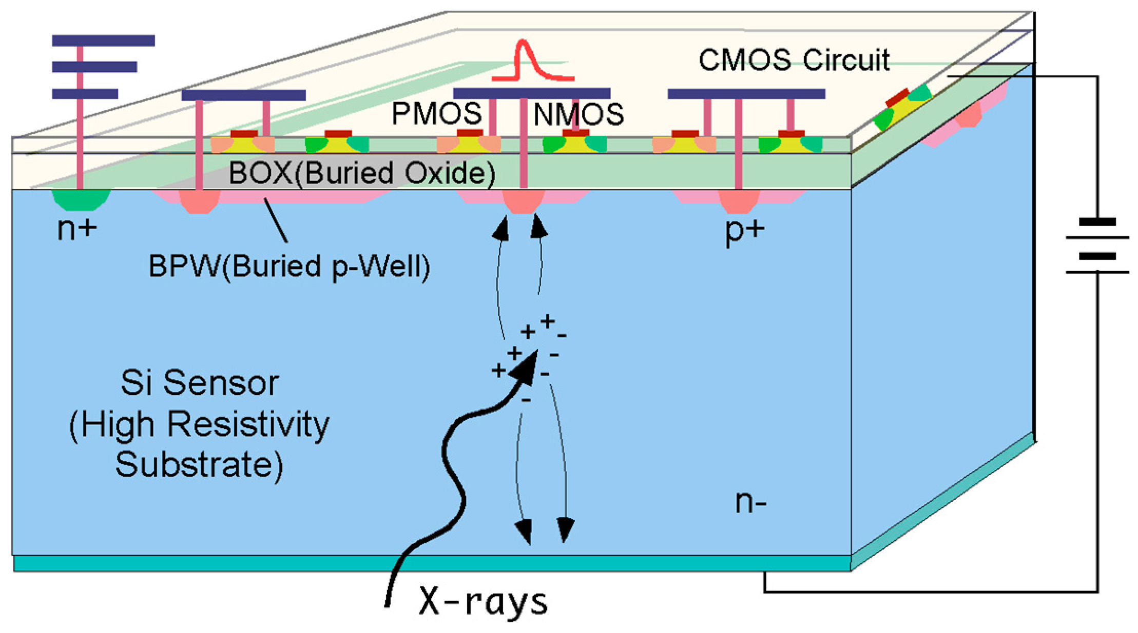
2. SOI Pixel Detector Using a Pinned Depleted Diode Structure
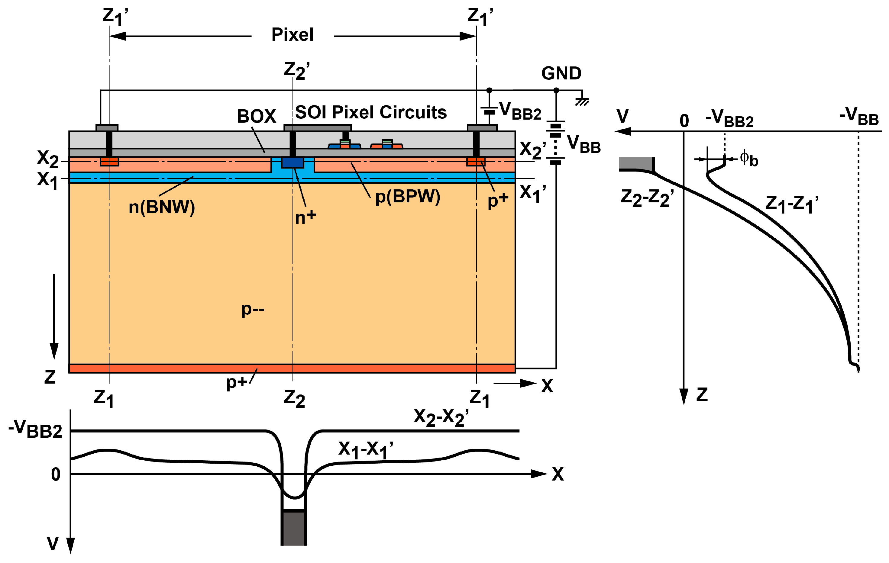
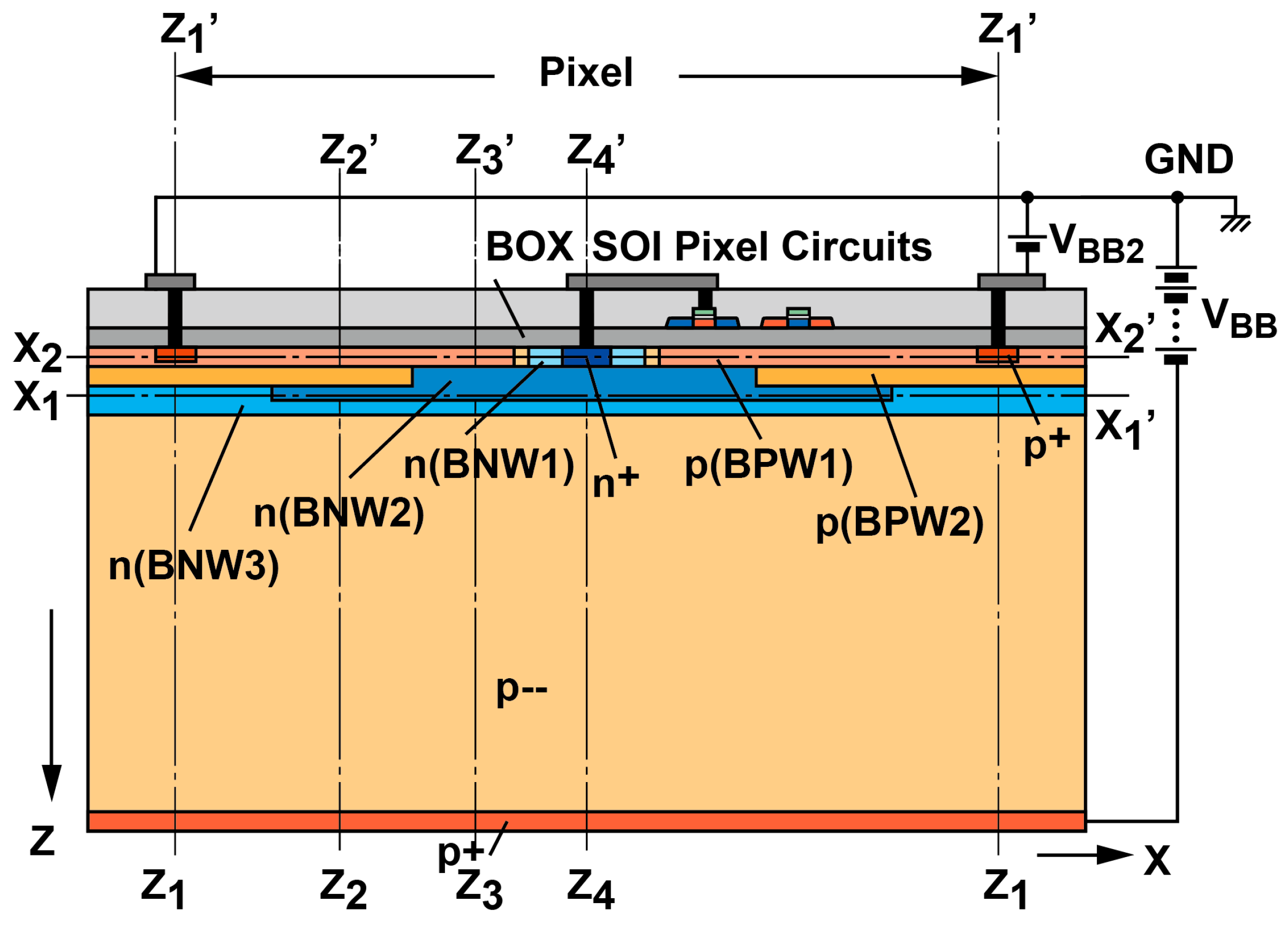
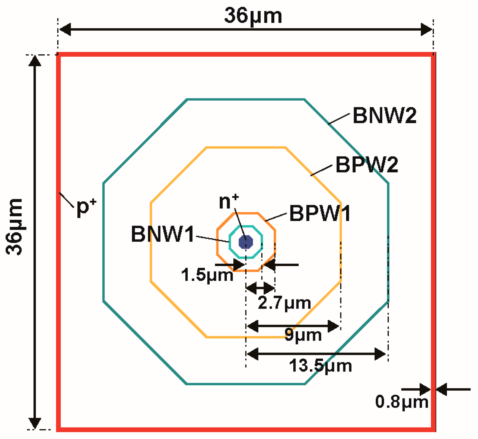
2.1. Sensor Structure Implemented on High-Resistivity Substrate
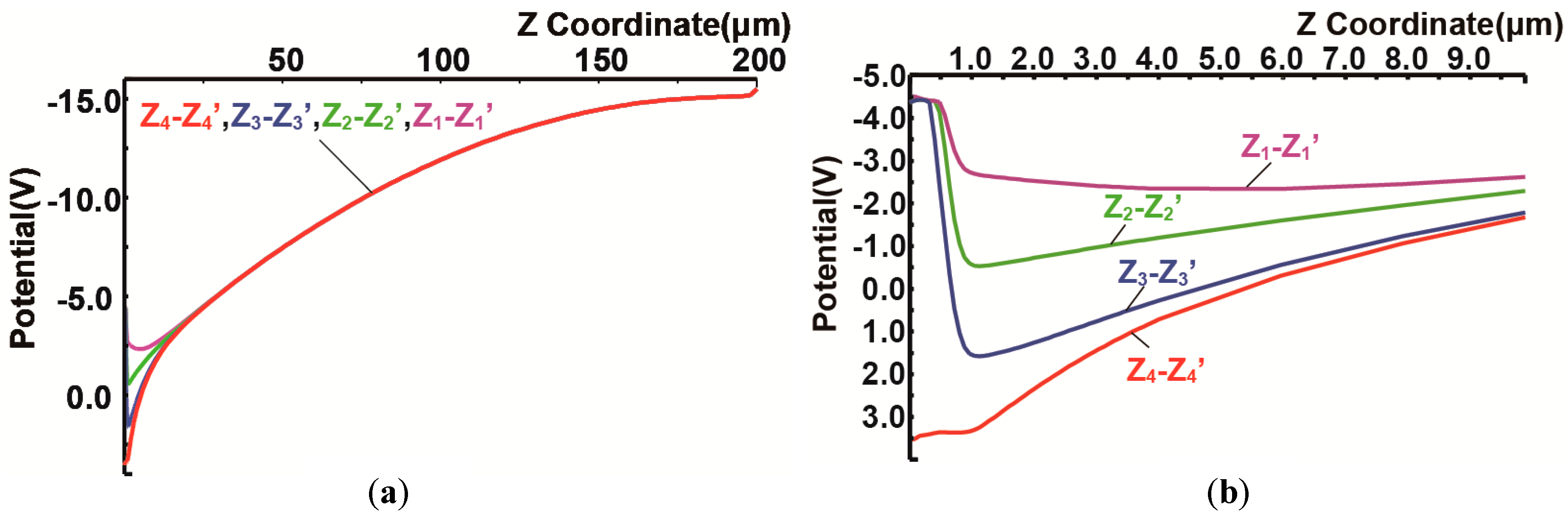
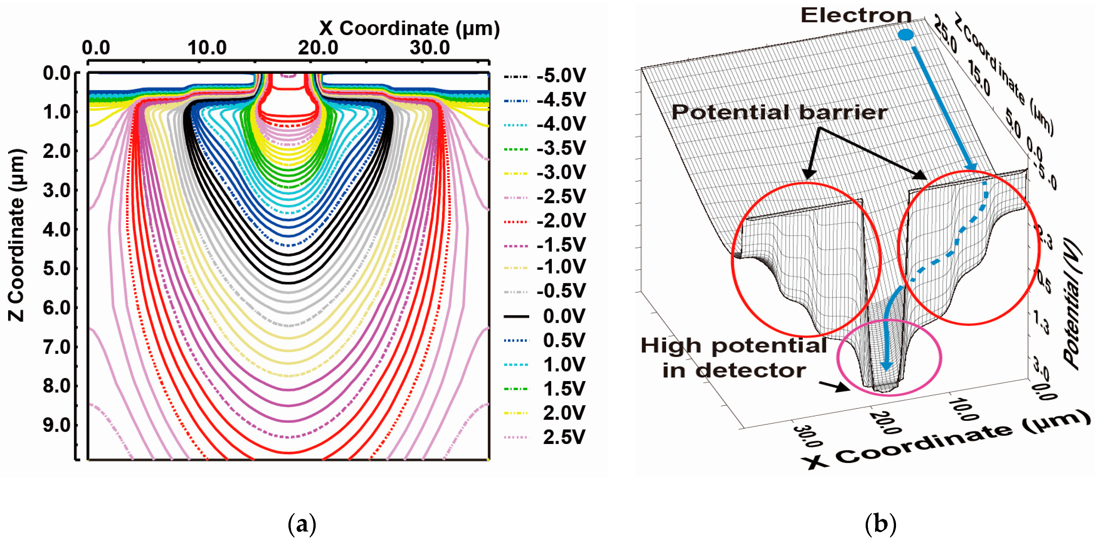
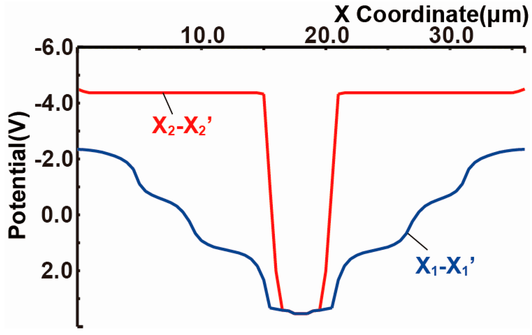
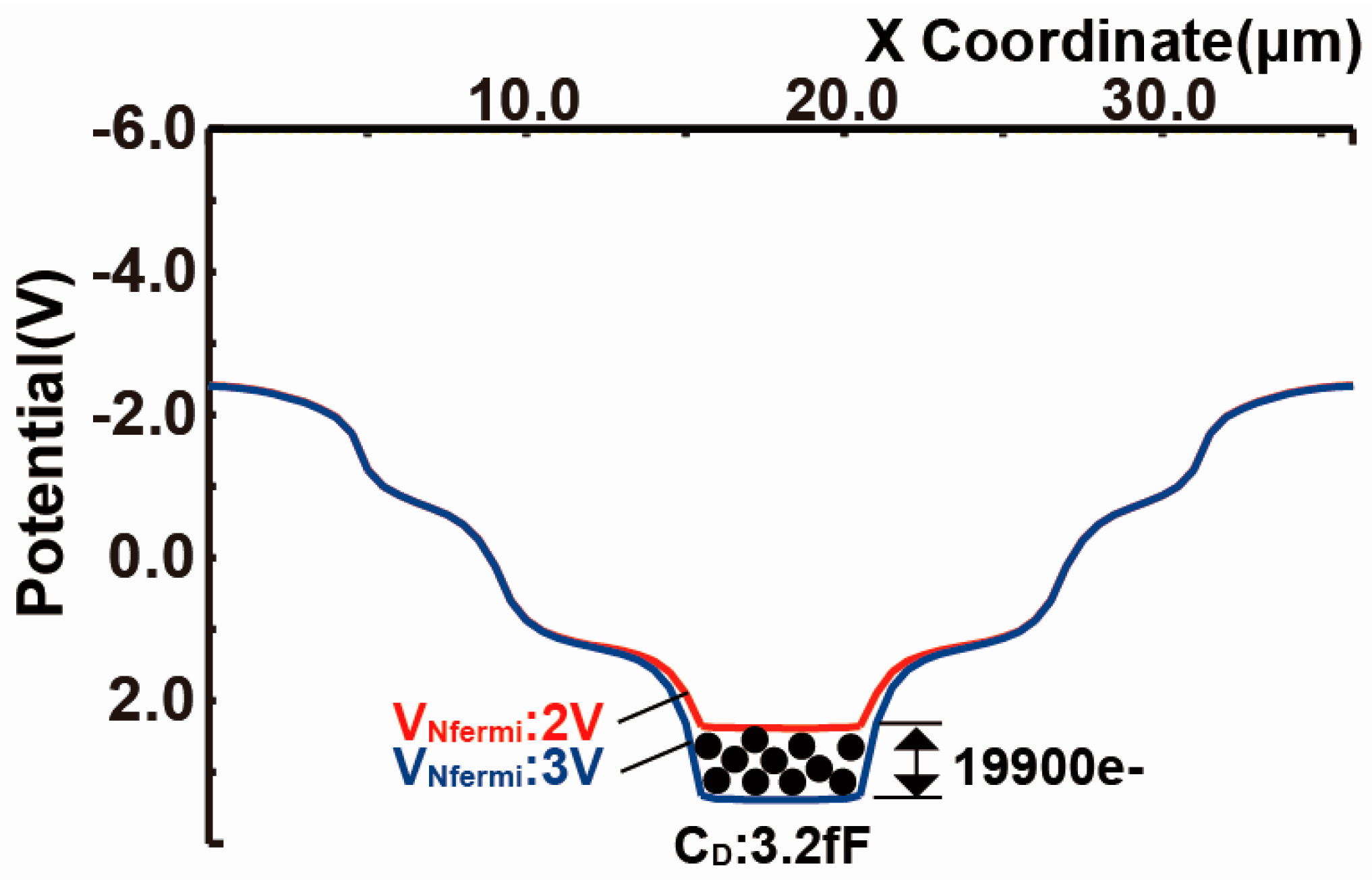
2.2. Simulation of Potential Profiles of the Designed SOIPIX-PDD
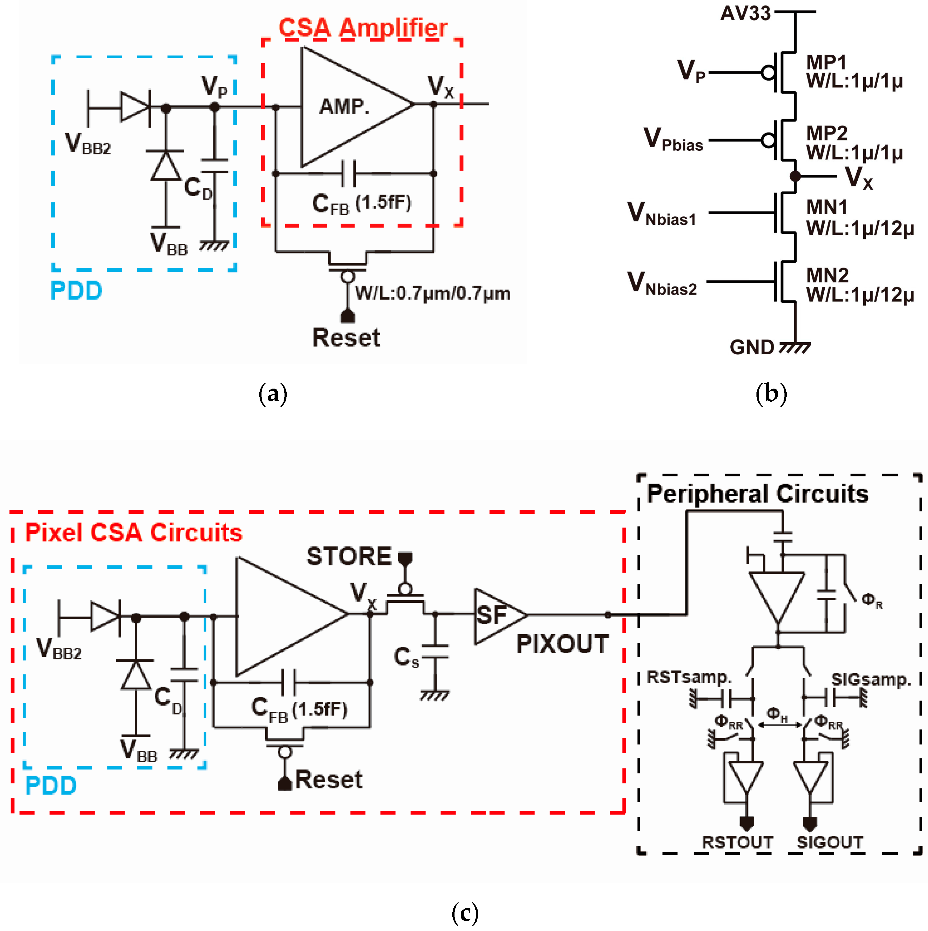
3. Charge-Sensitive Amplifier Design for Low-Noise Pixelated Detectors
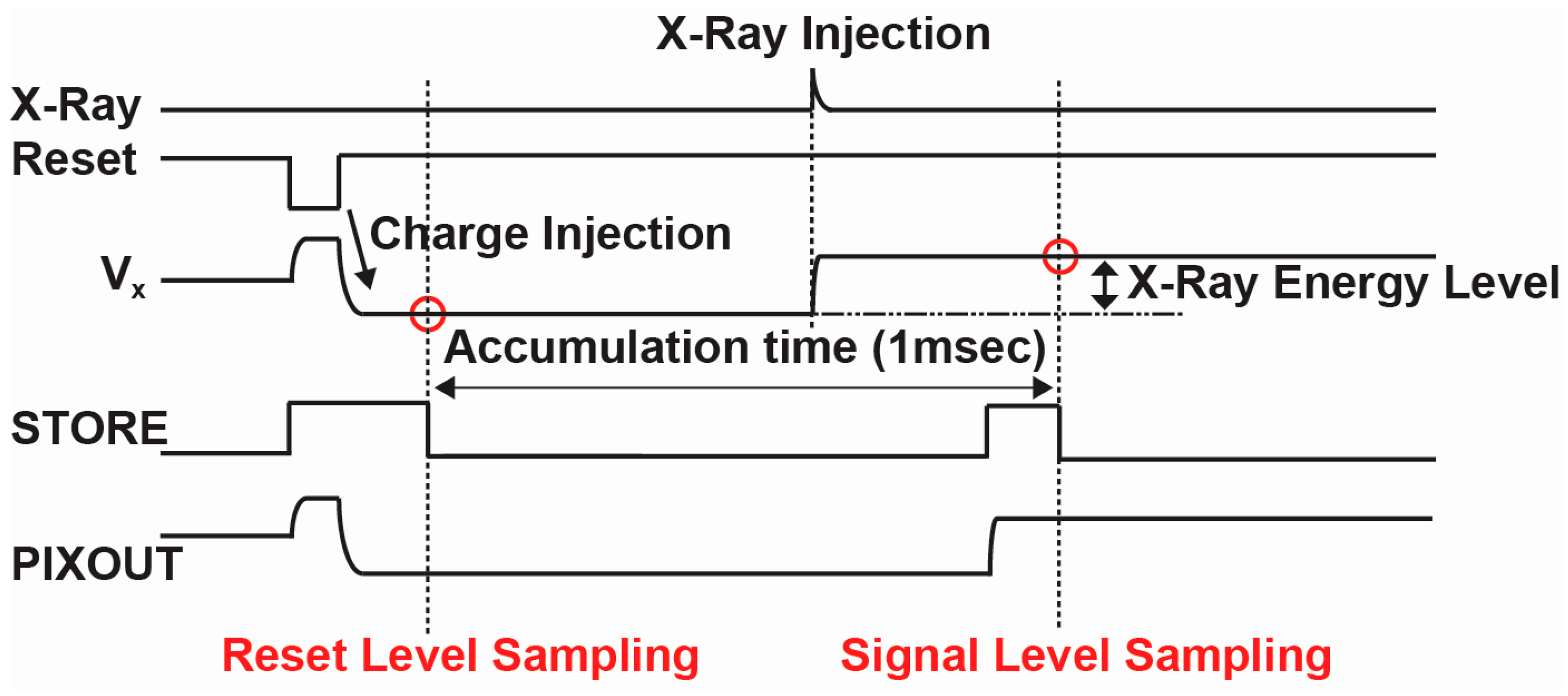
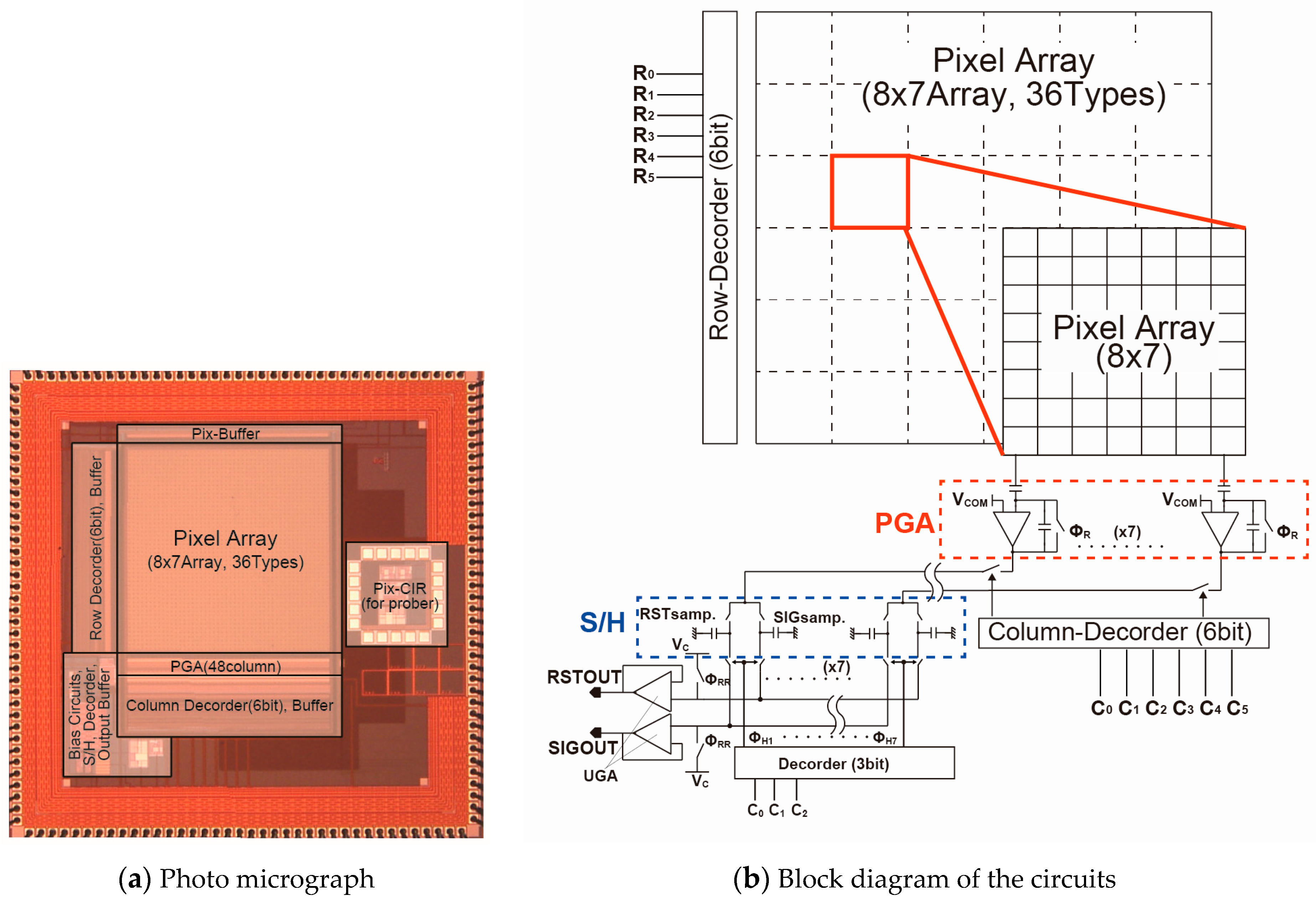
4. Implementation and Measurements
4.1. Basic Characteristics of the SOI Pxel with Pnned Depleted Diode Structure
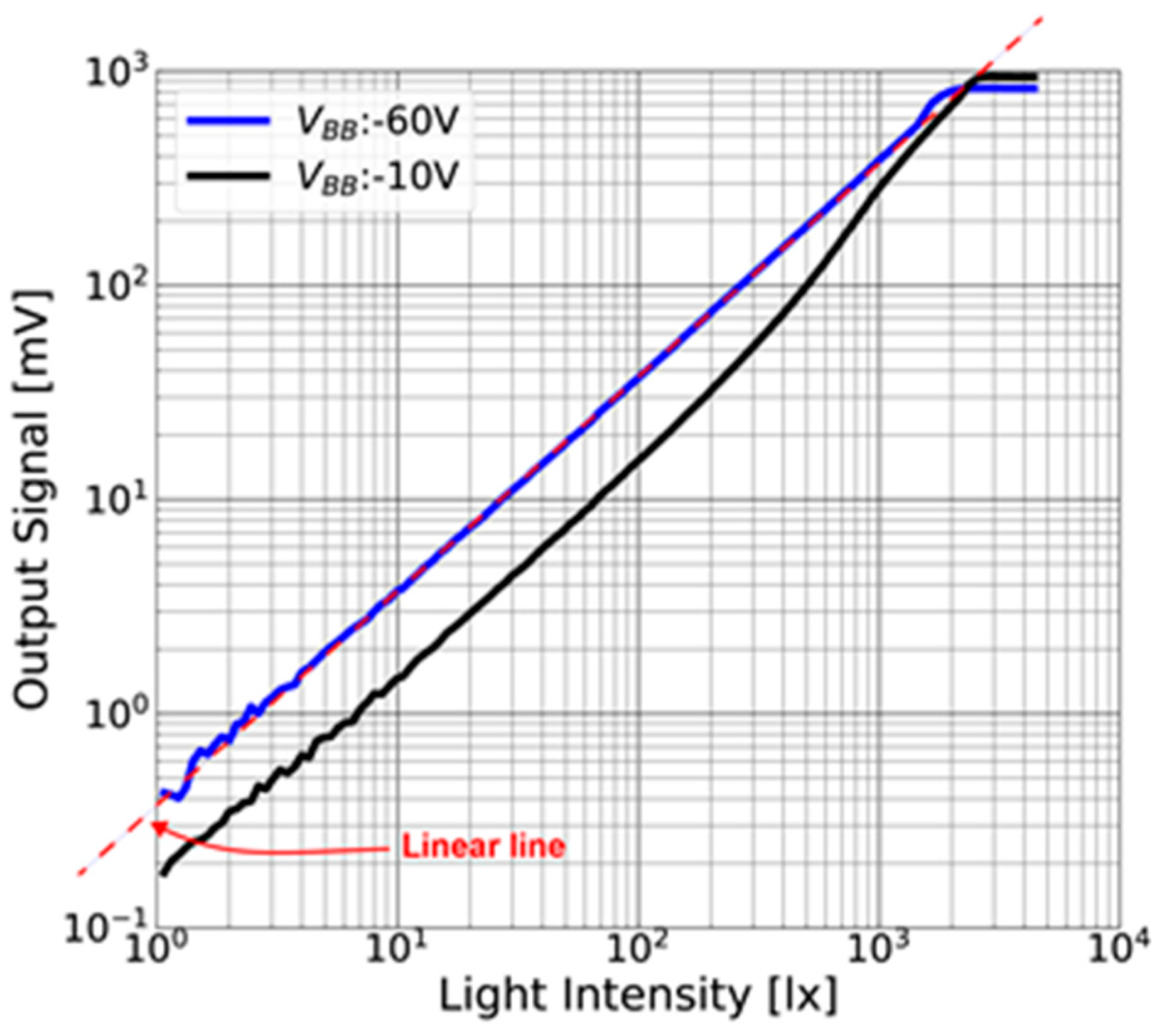
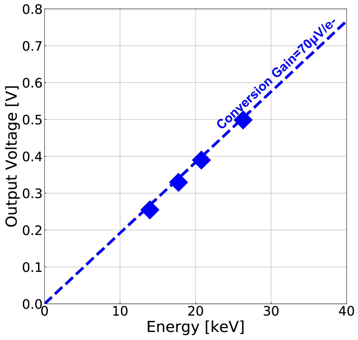
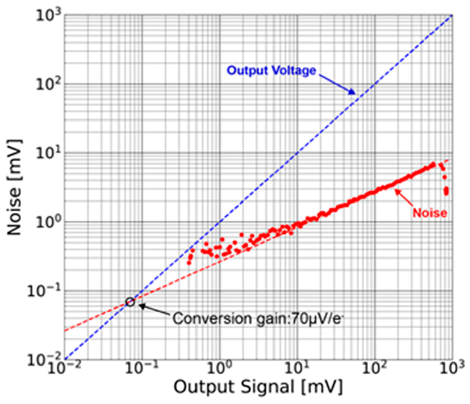
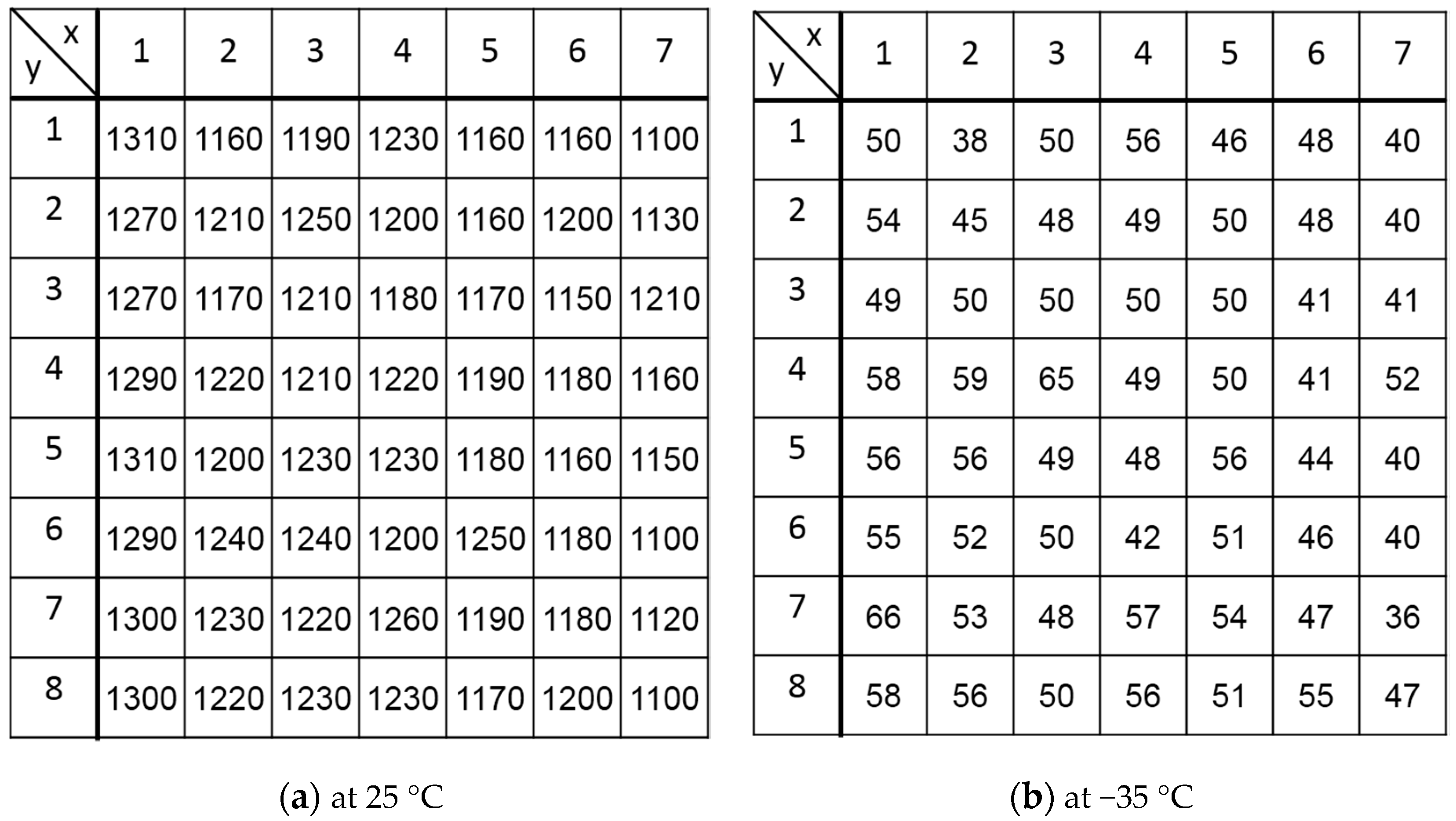
4.1.1. Linearity and Conversion Gain
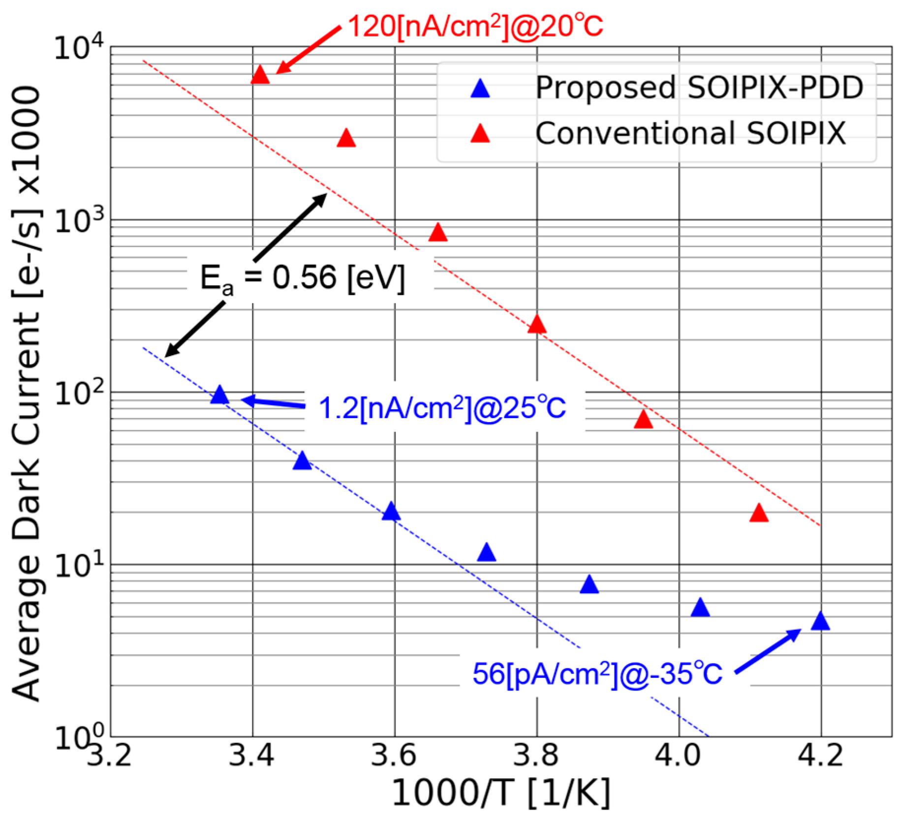
4.1.2. Dark Current
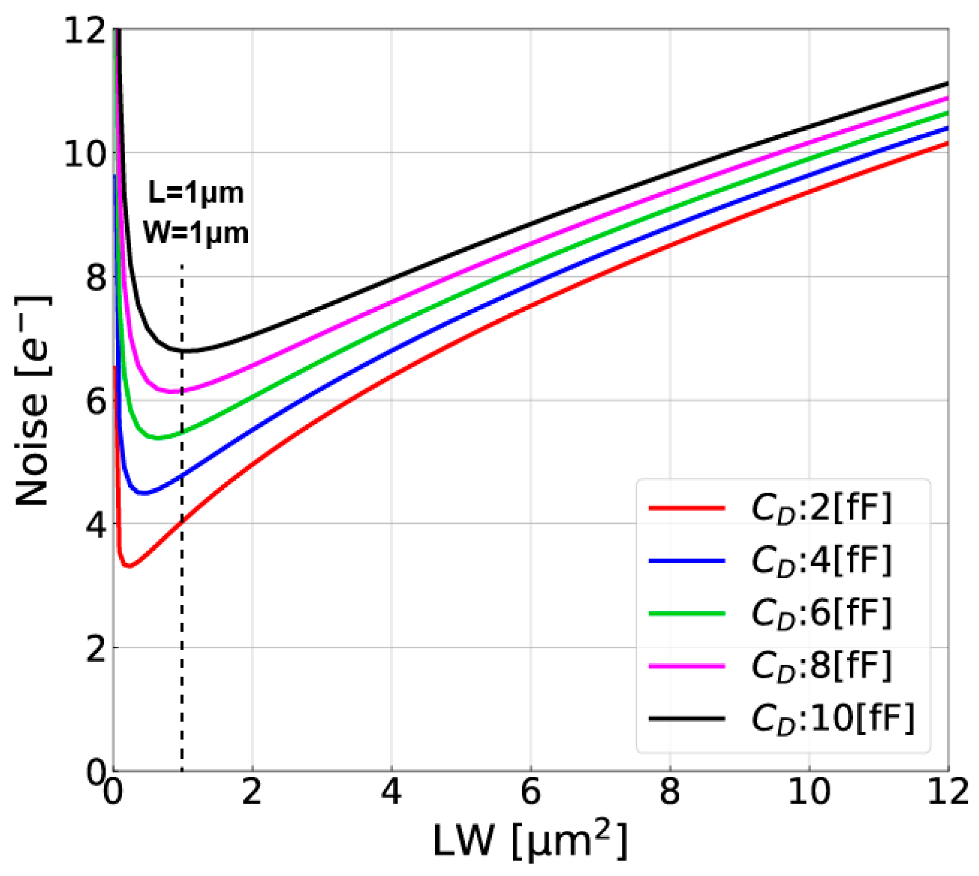
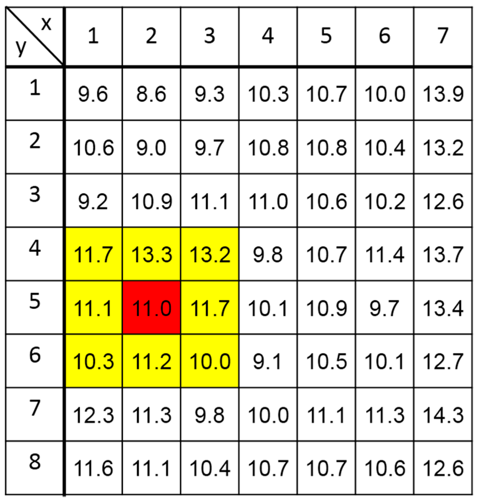
4.1.3 Readout Noise
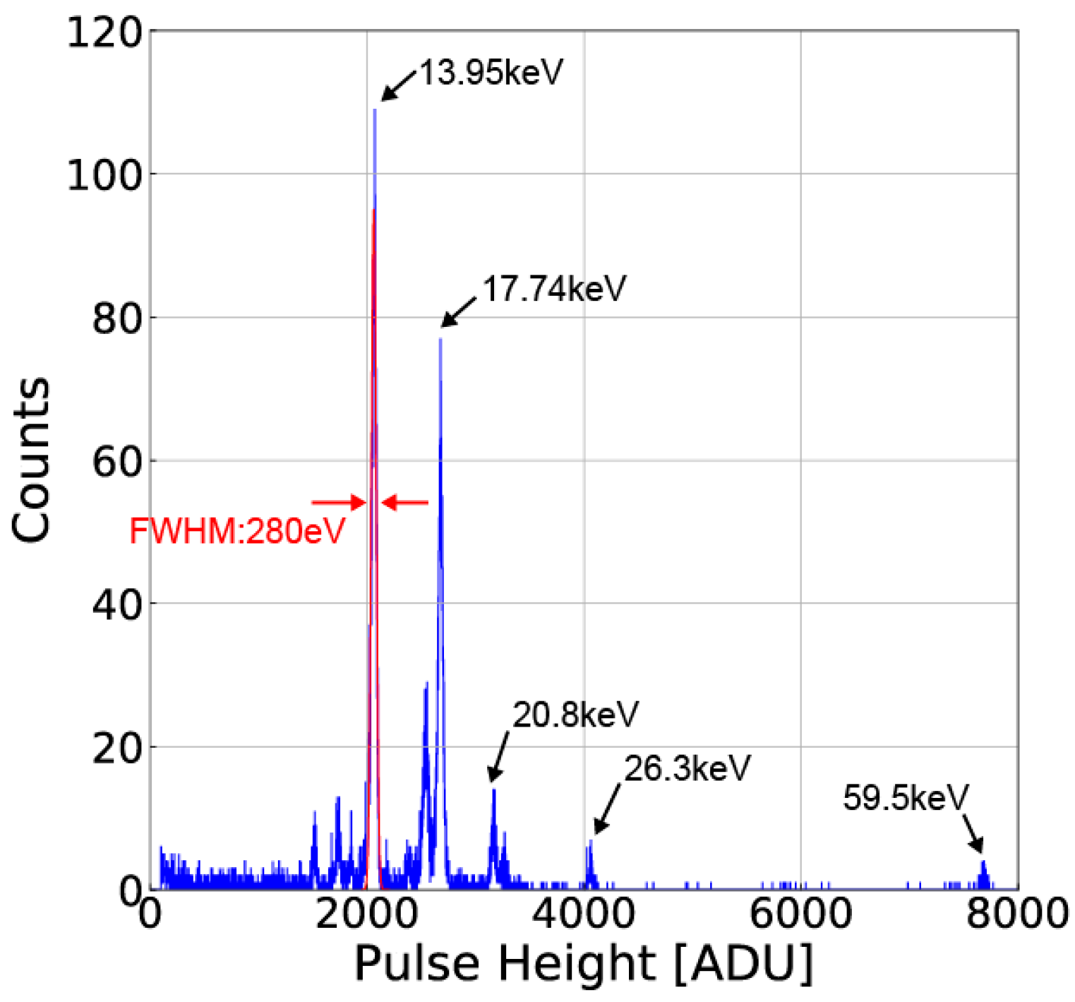
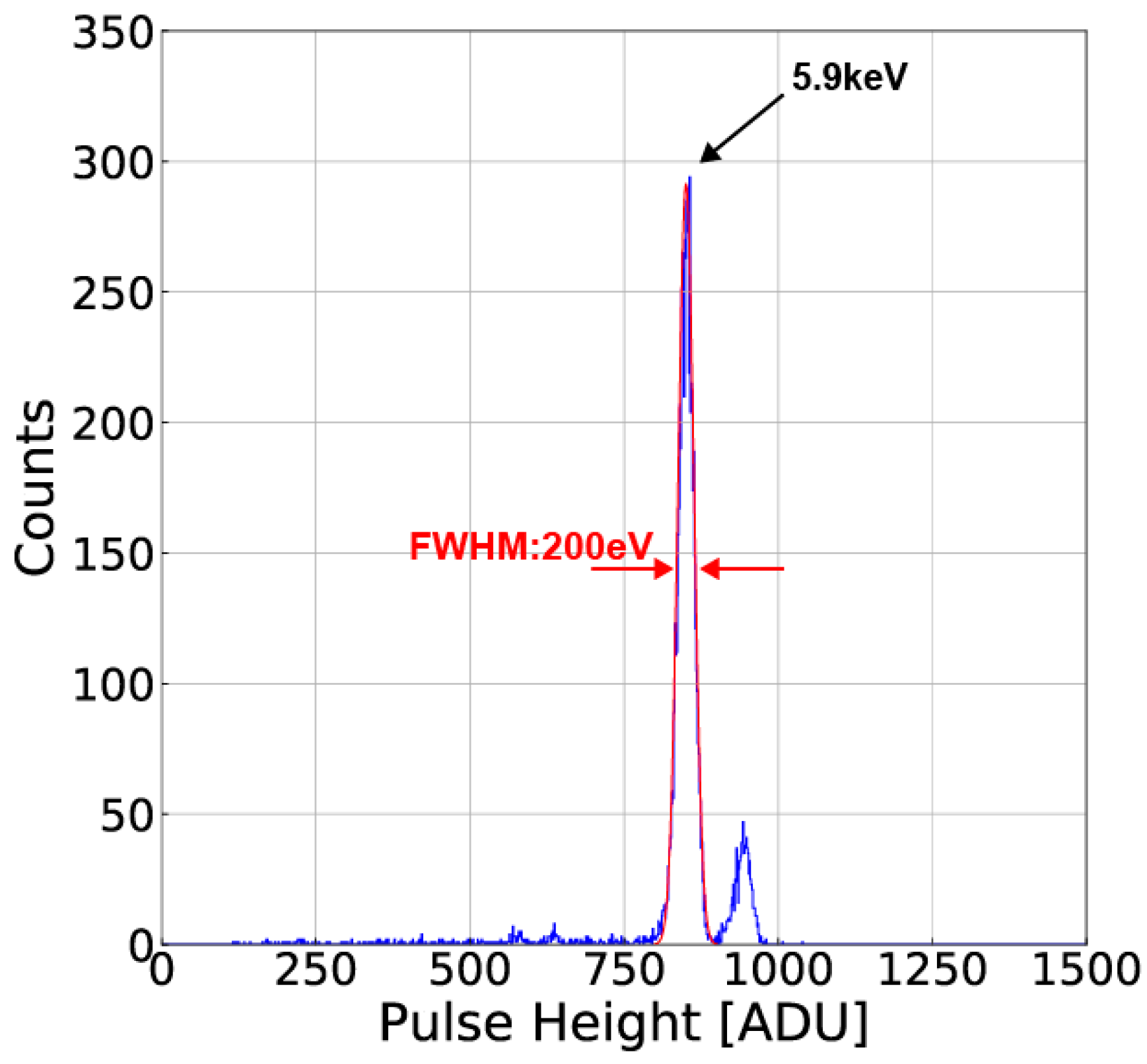
4.2. X-ray Eergy Sectrum
4.3. Performance Comparison
5. Conclusions
Acknowledgments
Author Contributions
Conflicts of Interest
References
- Koyama, K.; Tsunemi, H.; Dotani, T.; Bautz, M.W.; Hyashida, K.; Tsuru, T.G.; Matsumoto, H.; Ogawara, Y.; Ricker, G.R.; Doty, J.; et al. X-ray imaging spectrometer (XIS) on board Suzaku. Publ. Astron. Soc. Jpn. 2015, 59, 23–33. [Google Scholar] [CrossRef]
- Garmire, G.P.; Bautz, M.W.; Ford, P.G.; Nousek, J.A.; Ricker, G.R., Jr. Advanced CCD Imaging Spectrometer (ASICS) instrument on the Chandra X-ray Observatory. In X-ray and Gamma-ray Telescopes and Instruments for Astronomy; Trumper, J.E., Tananbaum, H.D., Eds.; SPIE: Bellingham, WA, USA, 2003; pp. 28–44. [Google Scholar]
- Arai, Y.; Miyoshi, T.; Unno, Y.; Tsuboyama, T.; Terada, S.; Ikegami, Y.; Ichimiya, R.; Kohriki, T.; Tauchi, K.; Ikemoto, Y.; et al. Development of SOI pixel process technology. In Nuclear Instruments and Methods in Physics Research Section A: Accelerators, Spectrometers, Detectors and Associated Equipment; Elsevier: Amsterdam, The Netherlands, 2011; Volume 636, pp. S31–S36. [Google Scholar]
- Griffith, C.V.; Falcon, A.D.; Prieskorn, Z.R.; Burrows, D.N. Speedster-EXD: A new event-driven hybrid CMOS X-ray detector. J. Astron. Telesc. Inst. 2016, 2, 1–13. [Google Scholar] [CrossRef]
- Arai, Y.; Miyoshi, T.; Unno, Y.; Tsuboyama, T.; Terada, S.; Ikegami, Y.; Kohriki, T.; Tauchi, K.; Ilemoto, Y.; Ichimiya, R.; Ikeda, H.; et al. Development of SOI monolithic pixel detectors. In Nuclear Instruments and Methods in Physics Research Section A: Accelerators, Spectrometers, Detectors and Associated Equipment; Elsevier: Amsterdam, The Netherlands, 2010; Volume 623, pp. 186–188. [Google Scholar]
- Nakashima, S.; Ryu, S.G.; Tsuru, T.G.; Takeda, A.; Arai, Y.; Miyoshi, T.; Ichimiya, R.; Ikemoto, Y.; Imamura, T.; Ohmoto, T.; et al. Progress in development of monolithic active pixel detector for X-ray astronomy with SOI CMOS technology. Phys. Procedia 2012, 37, 1373–1380. [Google Scholar] [CrossRef]
- Tsuru, T.G.; Matsumura, H.; Takeda, A.; Tanaka, T.; Nakashima, S.; Arai, Y.; Mori, K.; Takenaka, R.; Nishioka, Y.; Takayoshi, K.; et al. Development and performance of Kyoto’s X-ray astronomical SOI pixel (SOIPIX) sensor. In Space Telescopes and Instrumentation 2014: Ultraviolet to Gamma Ray; International Society for Optics and Photonics: Montreal, QC, Canada, 2014. [Google Scholar]
- Takeda, A.; Arai, Y.; Ryu, S.G.; Nakashima, S.; Tsuru, T.G.; Imamura, T.; Ohmoto, T.; Iwata, A. Design and evaluation of an SOI pixel sensor for trigger-driven X-ray readout. IEEE Trans. Nucl. Sci. 2013, 60, 586–591. [Google Scholar] [CrossRef]
- Takeda, A.; Tsuru, T.G.; Tanaka, T.; Uchida, H.; Matsumura, H.; Arai, Y.; Mori, K.; Nishioka, Y.; Takenaka, R.; Kohmura, T. Improvement of spectroscopic performance using a charge-sensitive amplifier circuit for an X-ray astronomical SOI pixel detector. J. Instrum. 2015, 10, C06005. [Google Scholar] [CrossRef]
- Okihara, M.; Kasai, H.; Miura, N.; Kuriyama, N.; Nagatomo, Y.; Hatsui, T.; Omodani, M.; Miyoshi, T.; Arai, Y. Progress of FD-SOI technology for monolithic pixel detectors. In Proceedings of the 2012 IEEE Nuclear Science Symposium and Medical Imaging Conference (NSS/MIC), Anaheim, CA, USA, 27 October–3 November 2012; pp. 471–474. [Google Scholar]
- Hashimoto, R.; Arai, Y.; Igarashi, N.; Kumai, R.; Miyoshi, T.; Kishimoto, S. Test results of a counting type SOI device for a new X-ray area detector. In Proceedings of the AIP Conference; American Institute of Physics: Melville, NY, USA, 2016; p. 1741. [Google Scholar]
- Lauxtermann, S.; Vangapally, V. A Fully Depleted Backside Illuminated CMOS Imager with VGA Resolution and 15-micron Pixel Pitch. In Proceedings of the IEEE International Image Sensor Workshop, Snowbird, UT, USA, 12–16 June 2013. [Google Scholar]
- Hatsui, H.; Omodani, M.; Kudo, T.; Kobayashi, K.; Imamura, T.; Ohmoto, T.; Iwata, A.; Ono, S.; Kirihara, Y.; Kameshima, T.; et al. A direct detection X-ray CMOS image sensor with 500 μm thick high resistivity silicon. In Proceedings of the IEEE International Image Sensor Workshop, Snowbird, UT, USA, 12–16 June 2013. [Google Scholar]
- Sekiguchi, Y.; Arai, Y.; Hamagaki, H.; Gunji, T. Development of SOI pixel sensor for environmental radiation monitor. RIKEN Accel. Prog. Rep. 2014, 47, 231. [Google Scholar]
- Fahim, F.; Deptuch, G.; Holm, S.; Shenai, A.; Lipton, R. Monolithic active pixel matrix with binary counters ASIC with nested wells. J. Instrum. 2013, 8, C04008. [Google Scholar] [CrossRef]
- Kamehama, H.; Shrestha, S.; Yasutomi, K.; Kagawa, K.; Takeda, A.; Tsuru, T.G.; Arai, Y.; Kawahito, S. Fully depleted SOI pixel photo detectors with backgate surface potential pinning. In Proceedings of the IEEE International Image Sensor Workshop, Vaals, The Netherlands, 8–11 June 2015. [Google Scholar]
- Teranishi, N.; Kohno, A.; Ishihara, Y.; Arai, K. No image lag photodiode structure in the interline CCD image sensor. In Proceedings of the International Electron Devices Meeting, San Francisco, CA, USA, 13–15 December 1982; pp. 324–327. [Google Scholar]
- Kawahito, S.; Seo, M.W. Noise reduction effect of multiple-sampling-based signal-reduction circuits for ultra-low Noise CMOS image sensors. Sensors 2016, 16, 1867. [Google Scholar] [CrossRef] [PubMed]
- Kawahito, S.; Itoh, S. Noise calculation model and analysis of high-gain readout circuits for CMOS image sensors. In Proceedings of the Electronic Imaging, San Jose, CA, USA, 28–31 January 2008. [Google Scholar]
- Ryu, S.G.; Tsuru, T.G.; Nakashima, S.; Takeda, A.; Arai, Y.; Miyoshi, T.; Ichimiya, R.; Ikemoto, Y.; Matsumoto, H.; Imamura, T.; et al. First performance evaluation of an X-ray SOI pixel sensor for imaging spectroscopy and intra-pixel trigger. IEEE Trans. Nucl. Sci. 2011, 58, 2528–2536. [Google Scholar] [CrossRef]
- Image Sensors and Signal Processing for Digital Still Camera; Nakamura, J. (Ed.) CRC: Boca Raton, FL, USA, 2005; pp. 81–83. [Google Scholar]


| Process | 0.20 µm FD-SOI CMOS Technology with Substrate-Detector Process |
|---|---|
| Substrate thickness | 200 µm |
| Wafer type | FZ-p (Floating Zone, p-type) |
| Substrate Resistivity | >25 kΩcm |
| SOIPIX Type | XRPIX1 [20] | XRPIX2b-A [9] | XRPIX3b-CSA [9] | SOIPIX-PDD |
|---|---|---|---|---|
| Conversion gain | 3.56 | 7.0 | 17.8 | 70 |
| Readout noise | 129 e−rms | 68 e−rms | 35 e−rms | 11.0 e−rms |
| Dark current | N. A. | N. A. | 120 nA/cm2@25 °C | 1.2 nA/cm2@20 °C |
| Energy resolution ([email protected] keV) | N. A. | N. A. | 320 eV (5.4%) | 200 eV (3.6%) |
| Energy resolution ([email protected] keV) | 1500 eV (10.8%) | (~1500 eV)* | N. A. | 280 eV (2.0%) |
© 2017 by the authors. Licensee MDPI, Basel, Switzerland. This article is an open access article distributed under the terms and conditions of the Creative Commons Attribution (CC BY) license (http://creativecommons.org/licenses/by/4.0/).
Share and Cite
Kamehama, H.; Kawahito, S.; Shrestha, S.; Nakanishi, S.; Yasutomi, K.; Takeda, A.; Tsuru, T.G.; Arai, Y. A Low-Noise X-ray Astronomical Silicon-On-Insulator Pixel Detector Using a Pinned Depleted Diode Structure. Sensors 2018, 18, 27. https://doi.org/10.3390/s18010027
Kamehama H, Kawahito S, Shrestha S, Nakanishi S, Yasutomi K, Takeda A, Tsuru TG, Arai Y. A Low-Noise X-ray Astronomical Silicon-On-Insulator Pixel Detector Using a Pinned Depleted Diode Structure. Sensors. 2018; 18(1):27. https://doi.org/10.3390/s18010027
Chicago/Turabian StyleKamehama, Hiroki, Shoji Kawahito, Sumeet Shrestha, Syunta Nakanishi, Keita Yasutomi, Ayaki Takeda, Takeshi Go Tsuru, and Yasuo Arai. 2018. "A Low-Noise X-ray Astronomical Silicon-On-Insulator Pixel Detector Using a Pinned Depleted Diode Structure" Sensors 18, no. 1: 27. https://doi.org/10.3390/s18010027