Silicon Nitride Photonic Integration Platforms for Visible, Near-Infrared and Mid-Infrared Applications

 , , , , ,
Abstract
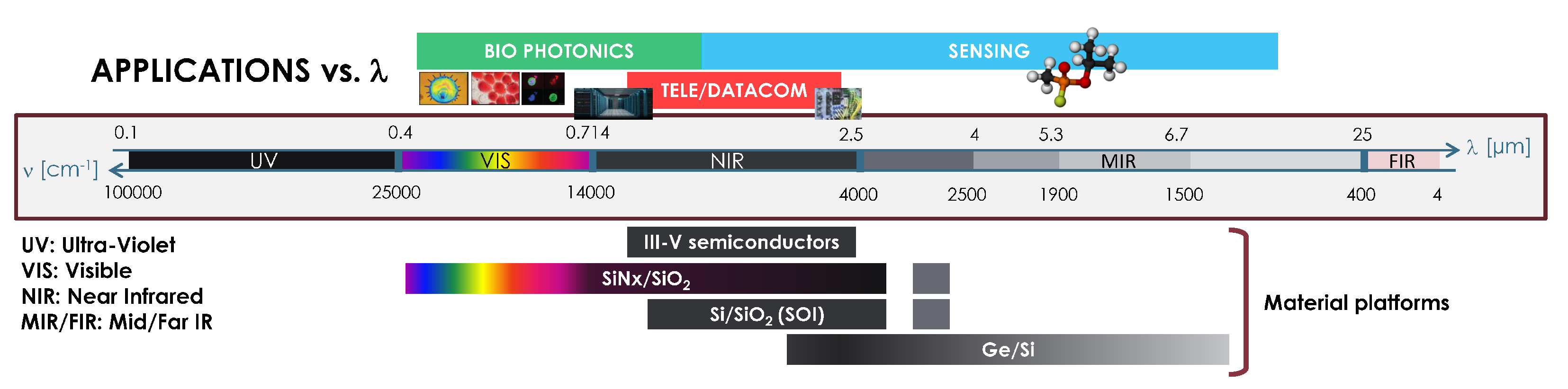
:1. Introduction
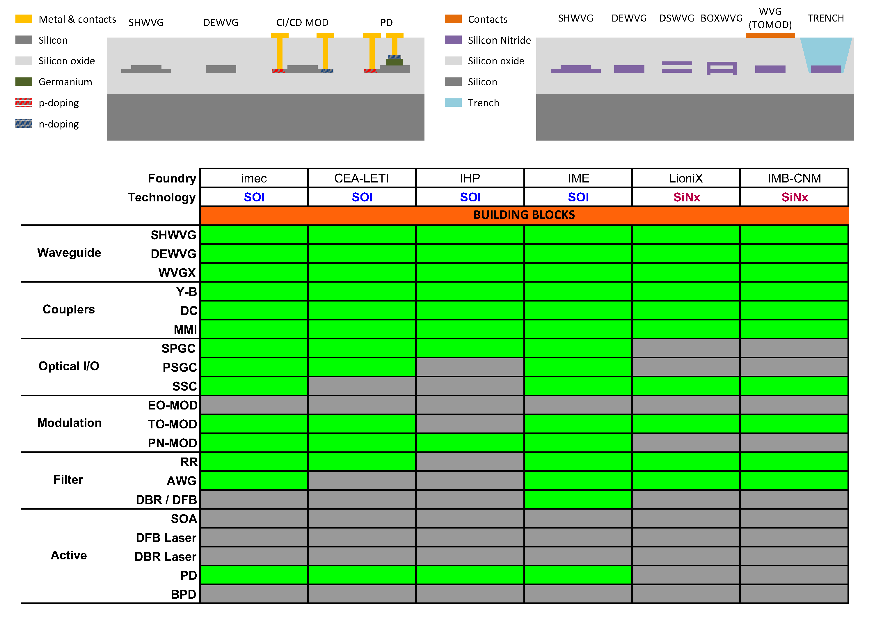
2. Silicon Nitride Photonic Integration Platforms: State of the Art
3. Silicon Nitride Platform With 300 nm Film Height
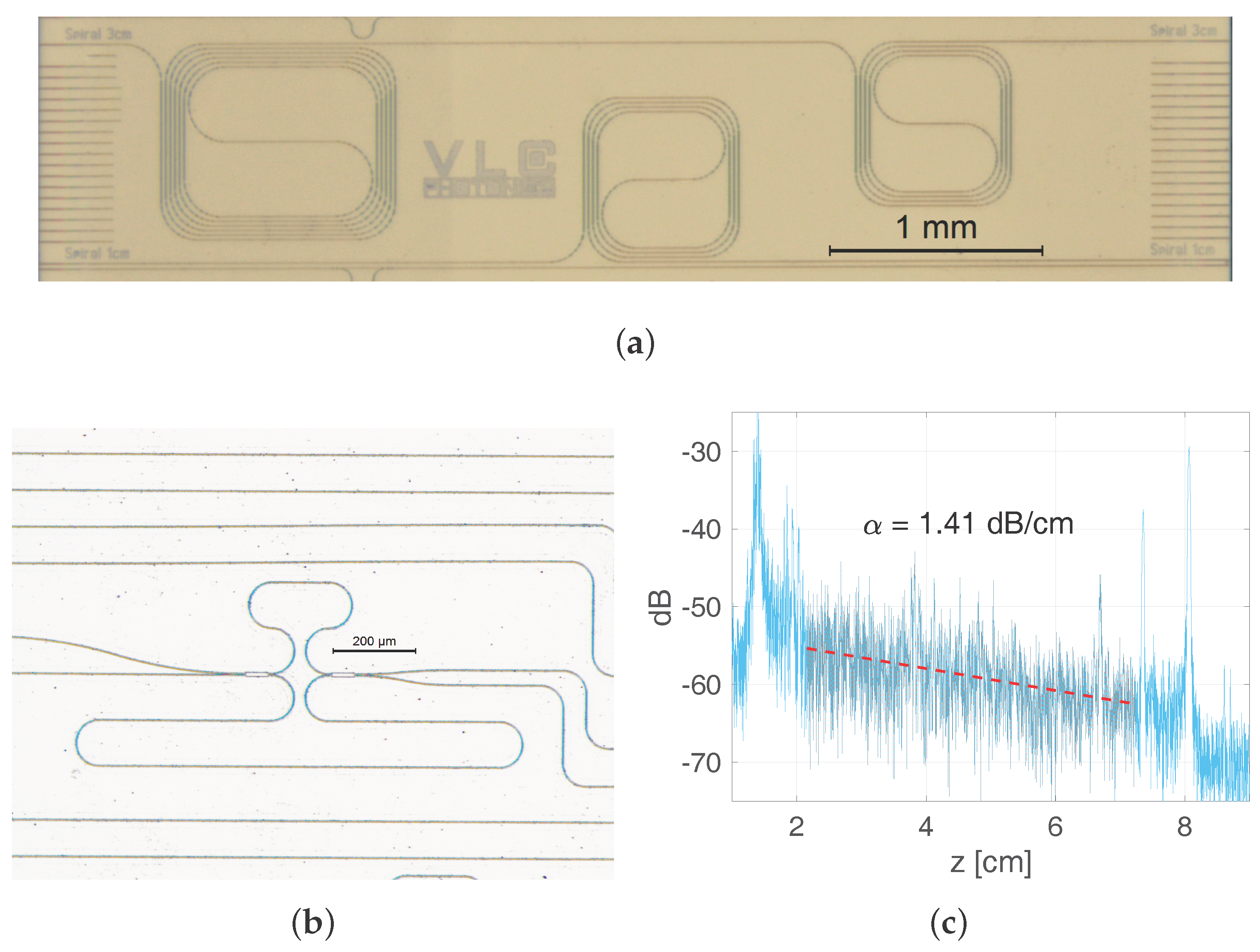
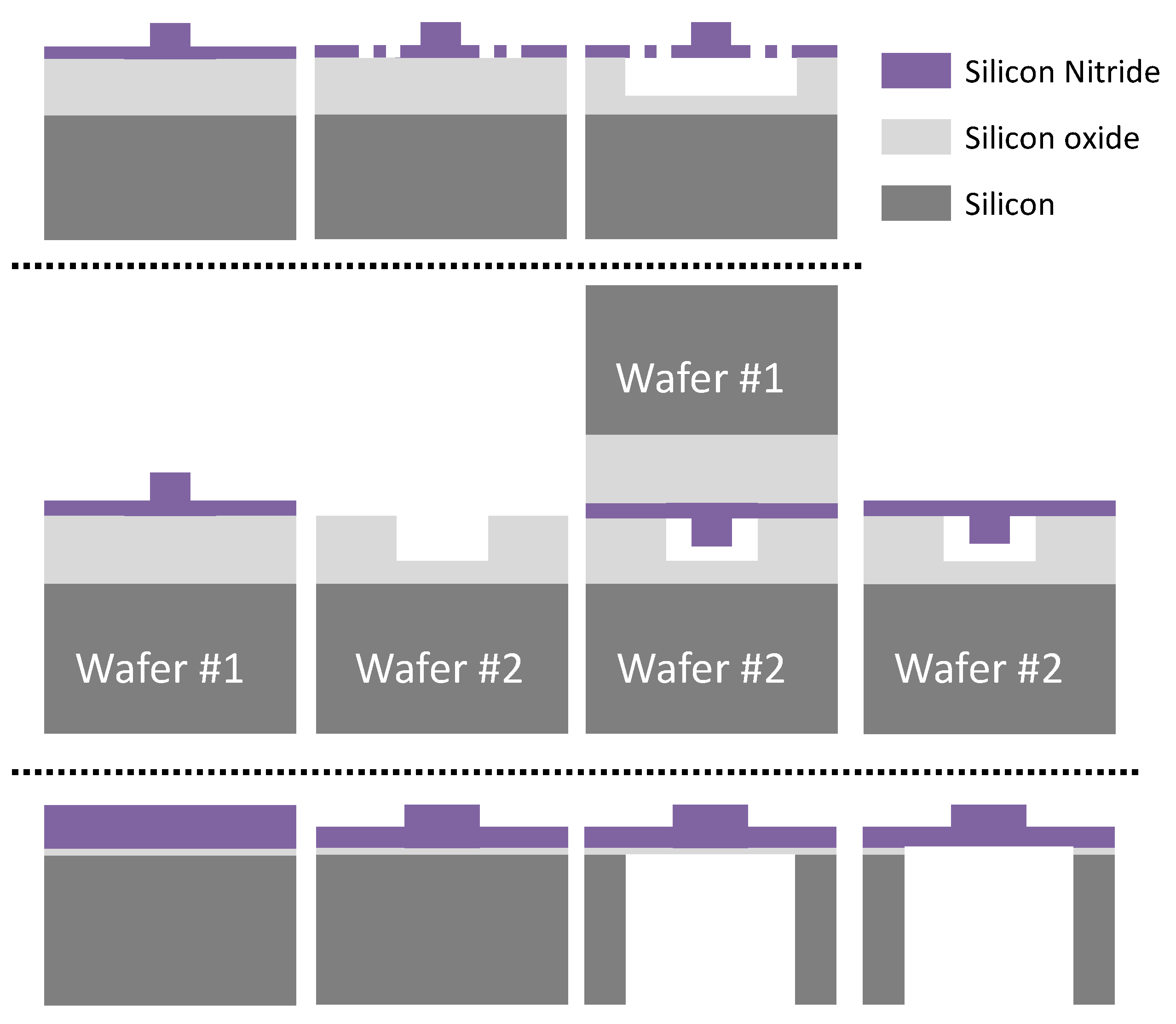
3.1. Fabrication Process
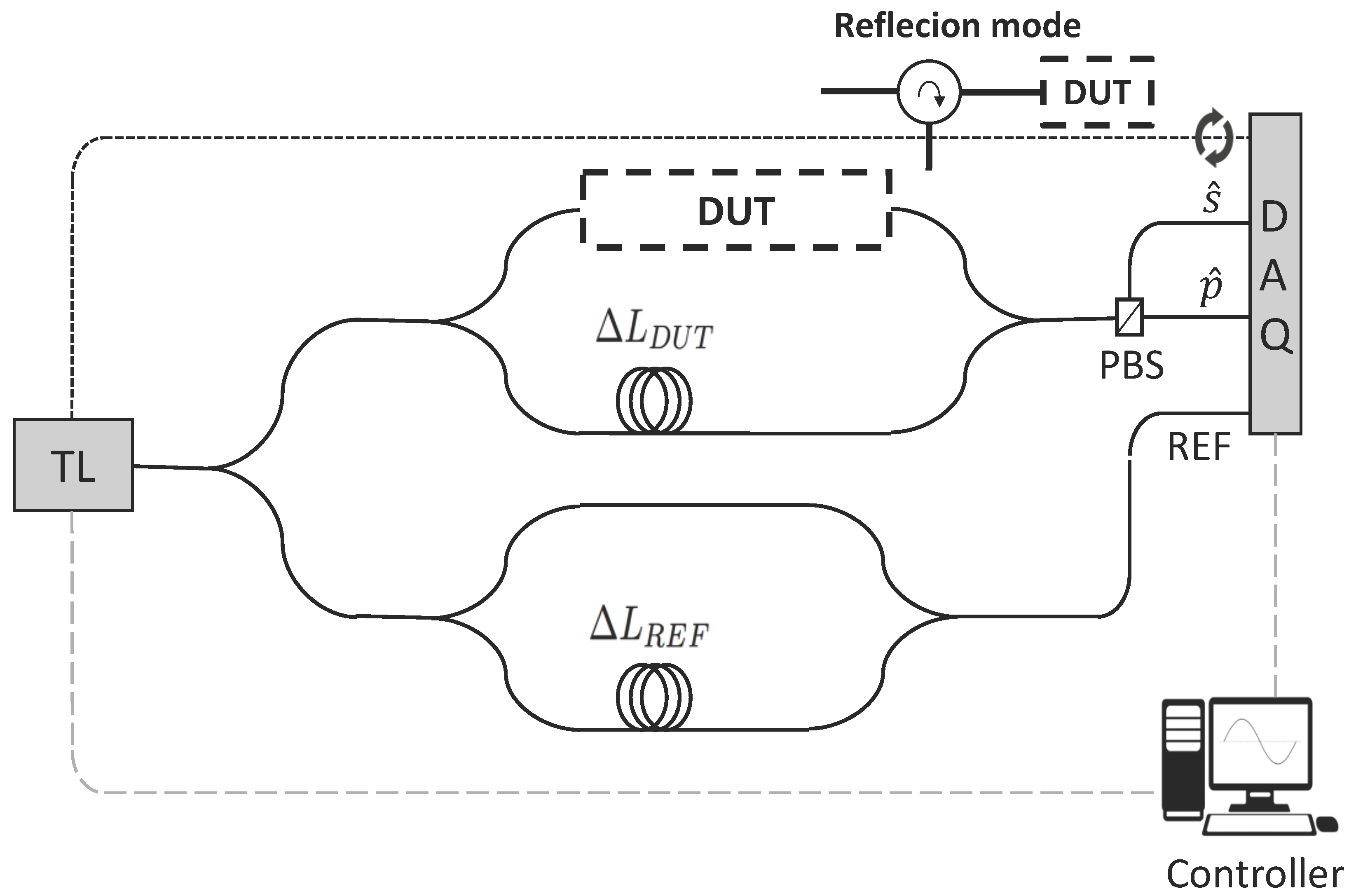
3.2. Measurement Setup
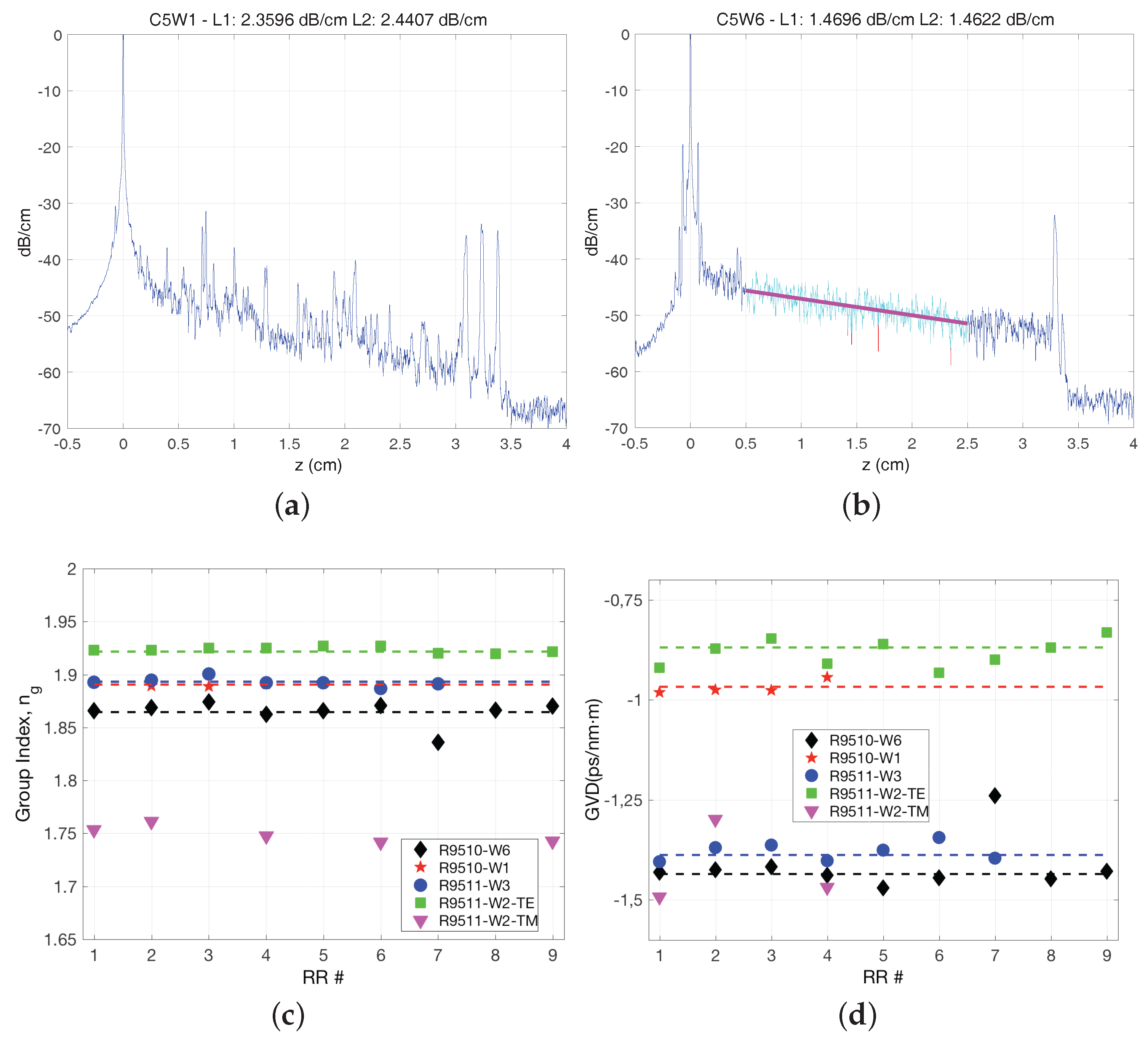
3.3. Propagation Loss
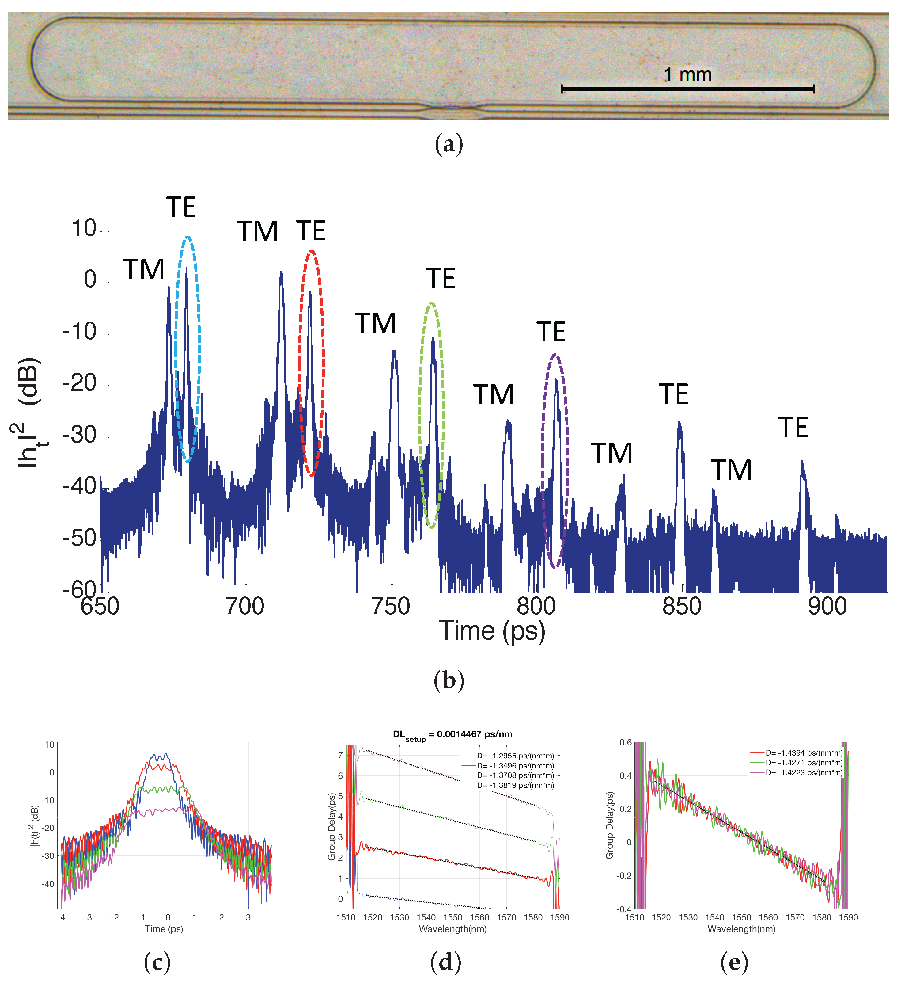
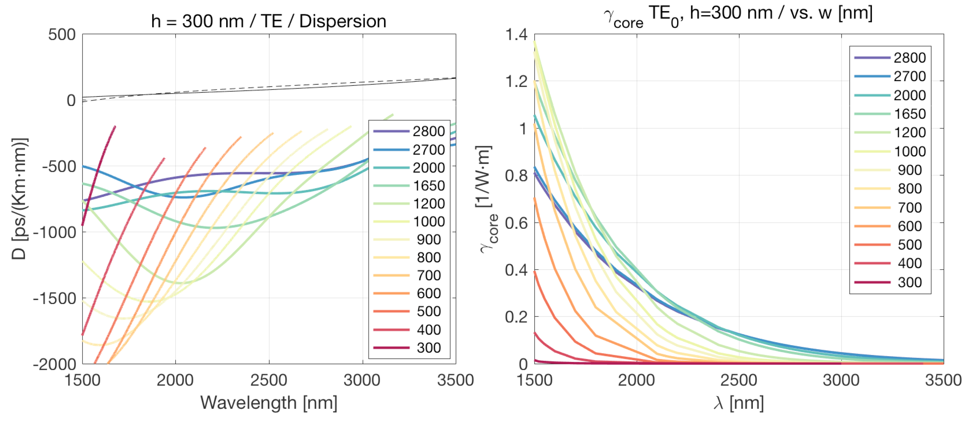
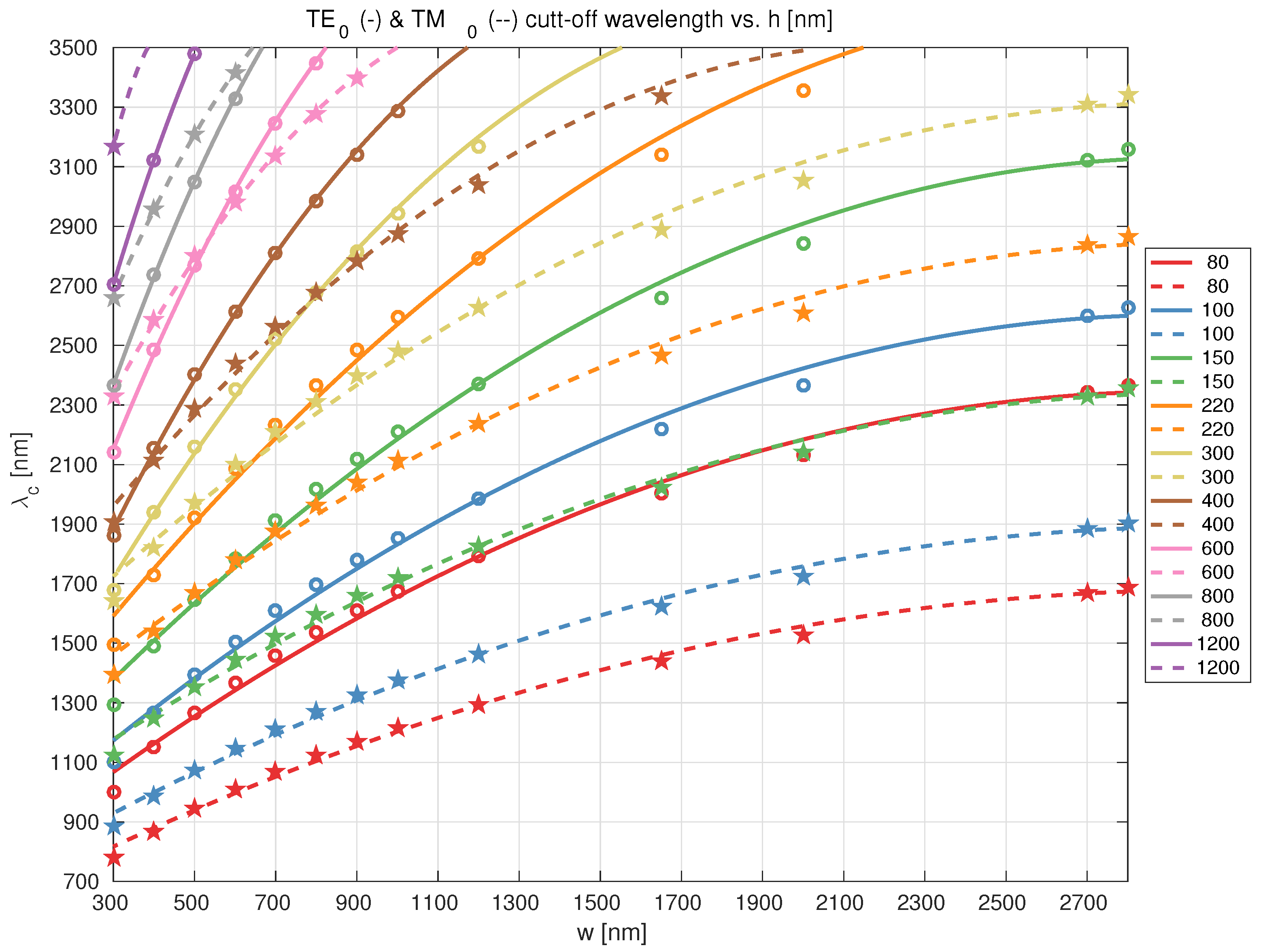
3.4. Group Index, Dispersion and Birefringence
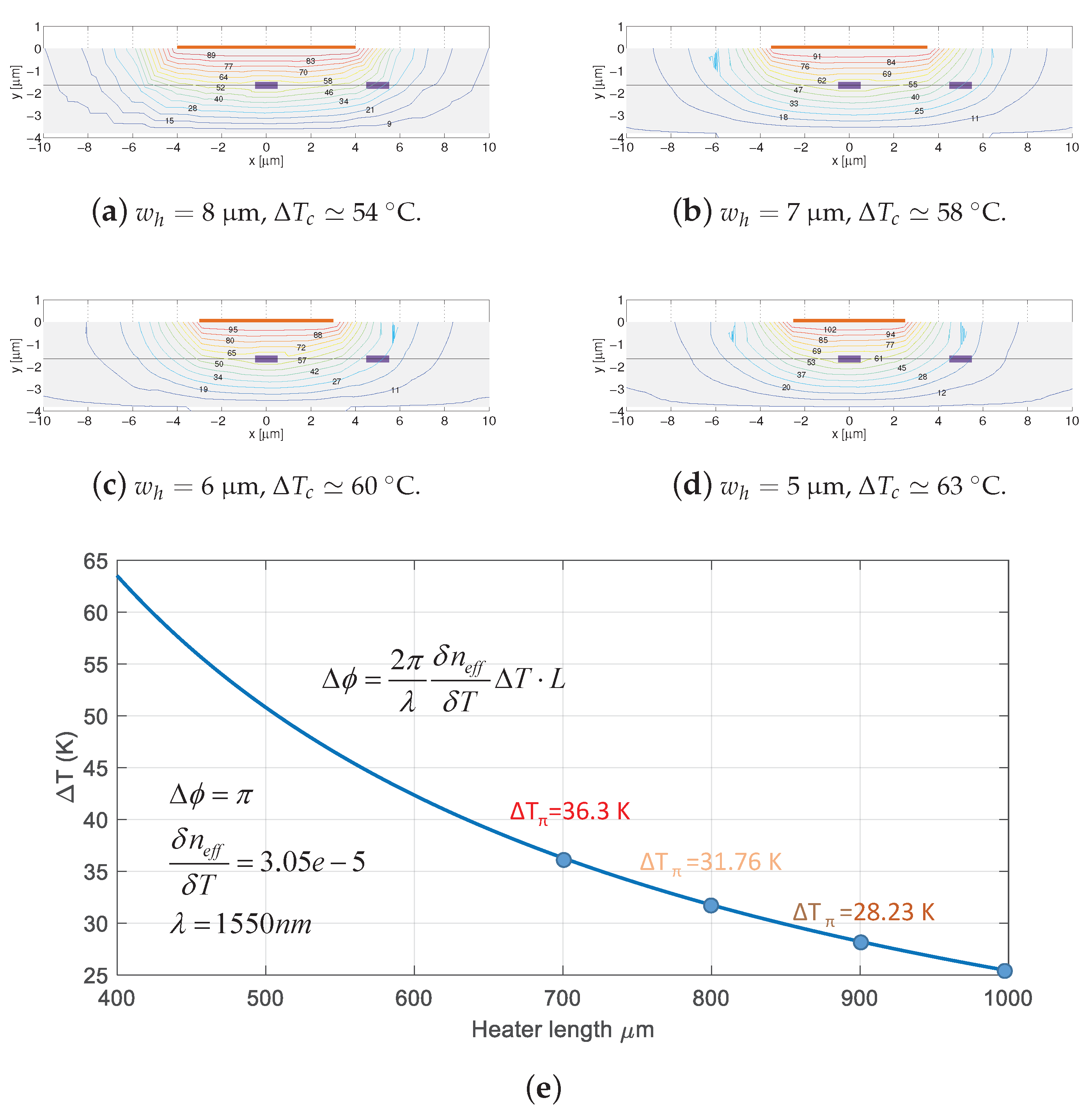
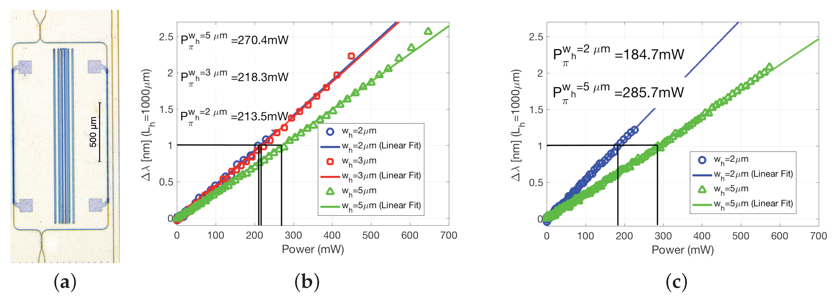
3.5. Thermo-Optic Phase Shifters
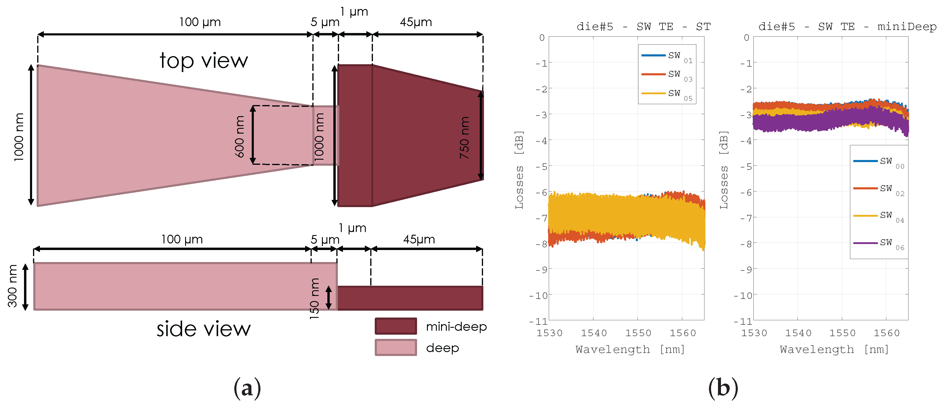
3.6. Fiber in/out Coupling Structures
3.7. Fabrication Process Steps Variations
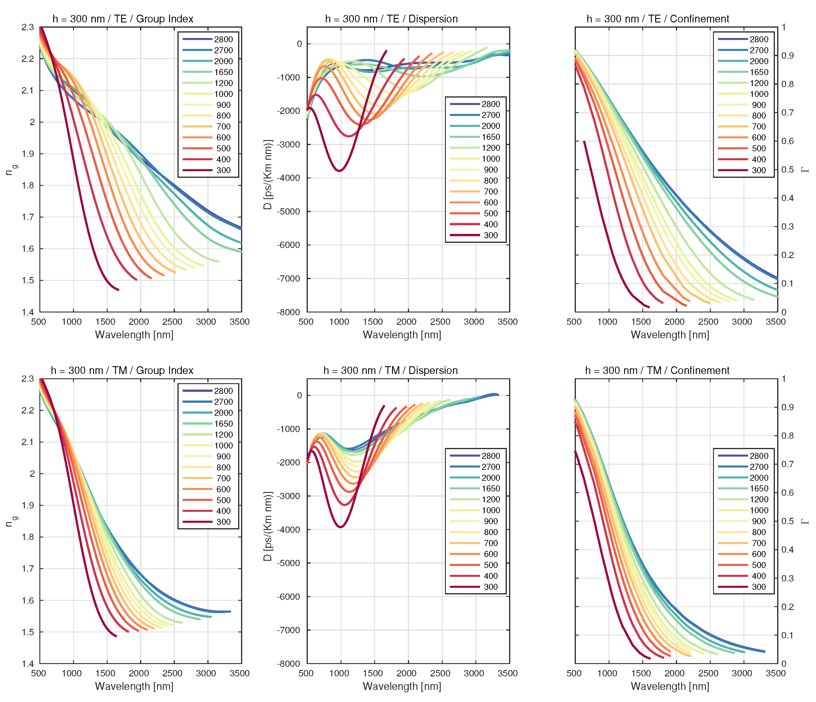
4. Prospects for Evolution
5. Conclusions
Acknowledgments
Author Contributions
Conflicts of Interest
Appendix A. Refractive Index Models

| [m] | 0.4 | 0.6 | 0.8 | 1 | 1.25 | 1.5 | 1.7 | 1.9 | 2.1 | 2.3 |
|---|---|---|---|---|---|---|---|---|---|---|
| 7.0 × 10 | 7.0 × 10 | 8.5 × 10 | 9.0 × 10 | 2.0 × 10 | 3.0 × 10 | 4.0 × 10 | 7.0 × 10 | 8.0 × 10 | 1.0 × 10 | |
| 2.5 | 2.75 | 2.85 | 3.0 | 3.1 | 3.15 | 3.3 | 3.5 | 3.75 | - | |
| 2.0 × 10 | 7.0 × 10 | 2.0 × 10 | 3.595 × 10 | 7.0 × 10 | 5.0 × 10 | 4.5 × 10 | 1.5 × 10 | 3.595 × 10 | - |
Appendix B. Numerical Simulation
Appendix C. Bernstein-Bézier Curve Fitting
Appendix C.1. Bernstein Polynomials
Appendix C.2. Effective Index, Group Index and Group Velocity Dispersion


Appendix C.3. Confinement and Non-Linear Coefficient
| h = 300 nm, TE | ||||||
| j↓ / i→ | 0 | 1 | 2 | 3 | 4 | 5 |
| 0 | 1.8776213 | 2.122918 | 1.8338975 | 2.1035948 | 1.9577628 | 1.9983654 |
| 1 | 1.5934236 | 2.0444746 | 1.5628135 | 1.9956184 | 1.7710133 | 1.8322354 |
| 2 | 1.4362759 | 2.1394231 | 1.3769242 | 2.1079449 | 1.7048331 | 1.8222323 |
| 3 | 1.1819761 | 1.6413274 | 1.7166467 | 1.404391 | 1.7171903 | 1.6057694 |
| 4 | 1.8481478 | 0.40673147 | 3.3983956 | 0.50210963 | 2.1211686 | 1.6983453 |
| 5 | 1.0641421 | 2.472913 | −0.55656357 | 3.0907673 | 0.83795738 | 1.5242143 |
| 6 | 1.6845798 | 0.71592265 | 2.9017514 | 0.43428066 | 2.0751221 | 1.5781534 |
| 7 | 1.2956966 | 1.786315 | 0.68464599 | 2.0493862 | 1.1950669 | 1.4802472 |
| 8 | 1.4635626 | 1.2874377 | 1.7004149 | 1.2467895 | 1.5764815 | 1.4858896 |
| 9 | 1.3965793 | 1.4399491 | 1.3459126 | 1.4839961 | 1.4166315 | 1.4509043 |
| 10 | 1.3994648 | 1.3942841 | 1.4113342 | 1.4091712 | 1.4289707 | 1.4336455 |
| 11 | 1.3863866 | 1.3867627 | 1.3895039 | 1.3997934 | 1.4072365 | 1.4142388 |
| h = 300 nm, TM | ||||||
| j↓ / i→ | 0 | 1 | 2 | 3 | 4 | 5 |
| 0 | 1.8887401 | 2.0011959 | 1.8974288 | 1.9885233 | 1.9436535 | 1.9559063 |
| 1 | 1.609455 | 1.8264855 | 1.6515491 | 1.8019914 | 1.7310931 | 1.7505446 |
| 2 | 1.4640987 | 1.8261739 | 1.486507 | 1.802394 | 1.6385824 | 1.6865425 |
| 3 | 1.0822236 | 1.5366187 | 1.2886216 | 1.4596529 | 1.4286029 | 1.4308623 |
| 4 | 2.048853 | 0.63601297 | 2.8696145 | 0.84074835 | 1.9212071 | 1.6511395 |
| 5 | 0.82208993 | 2.5255386 | −0.52650071 | 2.6367929 | 0.87419927 | 1.3632737 |
| 6 | 1.8738947 | 0.55886964 | 3.0985097 | 0.38808082 | 1.9833192 | 1.5423074 |
| 7 | 1.1896482 | 1.9091798 | 0.48595616 | 2.0705861 | 1.1322182 | 1.4061594 |
| 8 | 1.5039653 | 1.2294982 | 1.7920095 | 1.1714497 | 1.5558812 | 1.4495353 |
| 9 | 1.3849656 | 1.4550945 | 1.3147574 | 1.481189 | 1.3848654 | 1.4170576 |
| 10 | 1.3981807 | 1.3935368 | 1.4080525 | 1.396063 | 1.4087057 | 1.4083623 |
| 11 | 1.3810528 | 1.3913508 | 1.3786745 | 1.3942946 | 1.3896421 | 1.3937298 |
| h = 300 nm, TM | ||||||
| j↓ / i→ | 0 | 1 | 2 | 3 | 4 | 5 |
| 0 | 3.8362107 | 2.2956705 | −0.52159735 | 2.432606 | 0.13797359 | 0.68709093 |
| 1 | −0.71449253 | 2.7699387 | −2.6270367 | 2.2577456 | −0.4980362 | 0.21254014 |
| 2 | −1.1085944 | 5.5553406 | −7.0130271 | 5.9631147 | −1.8982644 | 0.34649937 |
| 3 | 1.4642427 | −10.343148 | 18.209874 | −15.298076 | 6.2120016 | −0.40174322 |
| 4 | −0.99087957 | 9.9119809 | −18.880421 | 17.320314 | −7.2764596 | 0.60477957 |
| 5 | 0.34561903 | −6.9986065 | 14.116331 | −13.41594 | 5.9589326 | −0.43974132 |
| 6 | 0.064912041 | 3.7130759 | −7.979316 | 7.990713 | −3.6080734 | 0.30824375 |
| 7 | −0.15910676 | −1.4492067 | 3.351523 | −3.5260698 | 1.6639435 | −0.13072975 |
| 8 | 0.096807226 | 0.3972896 | −1.0119507 | 1.1341267 | −0.54227326 | 0.05266007 |
| 9 | −0.031401585 | −0.068990285 | 0.20015457 | −0.23931782 | 0.12271787 | −0.0081222481 |
| 10 | 0.0050752322 | 0.0060853095 | −0.021668193 | 0.028655974 | −0.013077666 | 0.0030896597 |
| 11 | −0.00020783492 | 2.2365601 × 10 | 0.0002953014 | −0.00035186824 | 0.0012013796 | 0.0010157015 |
| h = 300 nm, TM | ||||||
| j↓ / i→ | 0 | 1 | 2 | 3 | 4 | 5 |
| 0 | 2.6208662 | 5.5999985 | −5.4884 | 6.2828556 | −1.3433512 | 0.7773674 |
| 1 | 2.781174 | 1.0400175 | 1.9201062 | −0.073226442 | 1.0902226 | 0.54736235 |
| 2 | −5.0616286 | 17.421036 | −24.023399 | 19.786281 | −7.0038343 | 0.84581743 |
| 3 | 4.6521823 | −19.935111 | 39.006147 | −32.76197 | 14.415252 | −0.53697909 |
| 4 | −3.3453677 | 11.697524 | −24.935911 | 24.847549 | −11.526451 | 0.87700597 |
| 5 | 2.0112132 | −3.8689726 | 9.4648453 | −10.411979 | 6.0538706 | −0.19157833 |
| 6 | −0.9336221 | −0.62343138 | −0.11605326 | 1.8652278 | −1.629988 | 0.15450445 |
| 7 | 0.30708937 | 1.6378095 | −2.5657901 | 1.4317783 | −0.024543856 | 0.079989325 |
| 8 | −0.061480214 | −0.99477548 | 1.708361 | −1.1694872 | 0.34468978 | 0.0032759916 |
| 9 | 0.004072112 | 0.32461521 | −0.58086131 | 0.44066724 | −0.11760206 | 0.031118024 |
| 10 | 0.00066290515 | −0.051610124 | 0.092767063 | −0.068004963 | 0.035175335 | 0.010901261 |
| 11 | −0.00046545281 | 0.0026939267 | −0.005011592 | 0.0057683831 | 0.0053385666 | 0.0083902458 |
References
- Macher, J.T.; Mowery, D.C. Vertical specialization and industry structure in high technology industries. In Business Strategy Over the Industry Lifecycle; Baum, J.A.C., McGahan, A.M., Eds.; Emerald Group Publishing Limited: Bingley, UK, 2004; pp. 317–355. [Google Scholar]
- Nenni, D.; McLellan, P.M. Fabless: The Transformation of the Semiconductor Industry; CreateSpace Independent Publishing Platform: Colorado Springs, CO, USA, 2014. [Google Scholar]
- Munoz, P. Photonic integration in the palm of your hand: Generic technology and multi-project wafers, technical roadblocks, challenges and evolution. In Proceedings of the 2017 Optical Fiber Communications Conference and Exhibition (OFC), Los Angeles, CA, USA, 19–23 March 2017; pp. 1–3. [Google Scholar]
- Lim, A.E.J.; Song, J.; Fang, Q.; Li, C.; Tu, X.; Duan, N.; Chen, K.K.; Tern, R.P.C.; Liow, T.Y. Review of silicon photonics foundry efforts. IEEE J. Sel. Top. Quantum Electron. 2014, 20, 405–416. [Google Scholar] [CrossRef]
- Smit, M.; Leijtens, X.; Ambrosius, H.; Bente, E.; Van der Tol, J.; Smalbrugge, B.; De Vries, T.; Geluk, E.J.; Bolk, J.; Van Veldhoven, R.; et al. An introduction to InP-based generic integration technology. Semiconduct. Sci. Technol. 2014, 29, 083001. [Google Scholar] [CrossRef]
- Leinse, A.; Heideman, R.; Hoekman, M.; Schreuder, F.; Falke, F.; Roeloffzen, C.; Zhuang, L.; Burla, M.; Marpaung, D.; Geuzebroek, D.; et al. TriPleX waveguide platform: Low-loss technology over a wide wavelength range. In Proceedings of Integrated Photonics: Materials, Devices, and Applications II.; SPIE: Bellingham, WA, USA, 2013; pp. 1–13. [Google Scholar]
- Kischkat, J.; Peters, S.; Gruska, B.; Semtsiv, M.; Chashnikova, M.; Klinkmüller, M.; Fedosenko, O.; Machulik, S.; Aleksandrova, A.; Monastyrskyi, G.; et al. Mid-infrared optical properties of thin films of aluminum oxide, titanium dioxide, silicon dioxide, aluminum nitride, and silicon nitride. Appl. Opt. 2012, 51, 6789–6798. [Google Scholar] [CrossRef] [PubMed]
- Malik, A.; Muneeb, M.; Shimura, Y.; Campenhout, J.V.; Loo, R.; Roelkens, G. Germanium-on-silicon mid-infrared waveguides and Mach-Zehnder interferometers. In Proceedings of the IEEE Photonics Conference, Bellevue, WA, USA, 8–12 September 2013; pp. 104–105. [Google Scholar]
- Malik, A.; Muneeb, M.; Pathak, S.; Shimura, Y.; Campenhout, J.V.; Loo, R.; Roelkens, G. Germanium-on-Silicon Mid-Infrared Arrayed Waveguide Grating Multiplexers. IEEE Photonics Technol. Lett. 2013, 25, 1805–1808. [Google Scholar] [CrossRef] [Green Version]
- Malik, A.; Muneeb, M.; Shimura, Y.; Campenhout, J.V.; Loo, R.; Roelkens, G. Germanium-on-silicon planar concave grating wavelength (de)multiplexers in the mid-infrared. Appl. Phys. Lett. 2013, 103, 161119. [Google Scholar] [CrossRef]
- Shen, L.; Healy, N.; Mitchell, C.J.; Penades, J.S.; Nedeljkovic, M.; Mashanovich, G.Z.; Peacock, A.C. Mid-infrared all-optical modulation in low-loss germanium-on-silicon waveguides. Opt. Lett. 2015, 40, 268–271. [Google Scholar] [CrossRef] [PubMed]
- Heck, M.J.R.; Bauters, J.F.; Davenport, M.L.; Doylend, J.K.; Jain, S.; Kurczveil, G.; Srinivasan, S.; Tang, Y.; Bowers, J.E. Hybrid Silicon Photonic Integrated Circuit Technology. IEEE J. Sel. Top. Quantum Electron. 2013, 19, 6100117. [Google Scholar] [CrossRef]
- Garces, I.; Villuendas, F.; Valles, J.A.; Dominguez, C.; Moreno, M. Analysis of leakage properties and guiding conditions of rib antiresonant reflecting optical waveguides. J. Lightw. Technol. 1996, 14, 798–805. [Google Scholar] [CrossRef]
- Krimmel, E.F.; Hezel, R. Si Silicon: Silicon Nitride in Microelectronics and Solar Cells; Springer: Berlin/Heidelberg, Germany, 1991. [Google Scholar]
- Stutius, W.; Streifer, W. Silicon nitride films on silicon for optical waveguides. Appl. Opt. 1977, 16, 3218–3222. [Google Scholar] [CrossRef] [PubMed]
- Heideman, R.G.; Kooyman, R.P.H.; Greve, J. Performance of a highly sensitive optical waveguide Mach-Zehnder interferometer immunosensor. Sens. Actuators B Chem. 1993, 10, 209–217. [Google Scholar] [CrossRef]
- Schipper, E.F.; Brugman, A.M.; Dominguez, C.; Lechuga, L.M.; Kooyman, R.P.H.; Greve, J. The realization of an integrated Mach-Zehnder waveguide immunosensor in silicon technology. Sens. Actuators B Chem. 1997, 40, 147–153. [Google Scholar] [CrossRef]
- Shaw, M.J.; Guo, J.; Vawter, G.A.; Habermehl, S.; Sullivan, C.T. Fabrication techniques for low-loss silicon nitride waveguides. In Proceedings of the Photonics West 2005, San Jose, CA, USA, 22–27 January 2005; SPIE: Bellingham, WA, 2005; pp. 109–118. [Google Scholar]
- Melchiorri, M.; Daldosso, N.; Sbrana, F.; Pavesi, L.; Pucker, G.; Kompocholis, C.; Bellutti, P.; Lui, A. Propagation losses of silicon nitride waveguides in the near-infrared range. Appl. Phys. Lett. 2005, 86, 121111. [Google Scholar] [CrossRef]
- Worhoff, K.; Klein, E.; Hussein, G.; Driessen, A. Silicon oxynitride based photonics. In Proceedings of the IEEE 10th Anniversary International Conference on Transparent Optical Networks, Athens, Greece, 22–26 June 2008; Volume 3, pp. 266–269. [Google Scholar]
- Mao, S.C.; Tao, S.H.; Xu, Y.L.; Sun, X.W.; Yu, M.B.; Lo, G.Q.; Kwong, D.L. Low propagation loss SiN optical waveguide prepared by optimal low-hydrogen module. Opt. Express 2008, 16, 20809–20816. [Google Scholar] [CrossRef] [PubMed]
- Bauters, J.F.; Heck, M.J.R.; John, D.; Dai, D.; Tien, M.C.; Barton, J.S.; Leinse, A.; Heideman, R.G.; Blumenthal, D.J.; Bowers, J.E. Ultra-low-loss high-aspect-ratio Si3N4 waveguides. Opt. Express 2011, 19, 3163–3174. [Google Scholar] [CrossRef] [PubMed]
- Bauters, J.F.; Heck, M.J.R.; John, D.D.; Barton, J.S.; Bruinink, C.M.; Leinse, A.; Heideman, R.G.; Blumenthal, D.J.; Bowers, J.E. Planar waveguides with less than 0.1 dB/m propagation loss fabricated with wafer bonding. Opt. Express 2011, 19, 24090–24101. [Google Scholar] [CrossRef] [PubMed]
- Romero-García, S.; Merget, F.; Zhong, F.; Finkelstein, H.; Witzens, J. Silicon nitride CMOS-compatible platform for integrated photonics applications at visible wavelengths. Opt. Express 2013, 21, 14036–14046. [Google Scholar] [CrossRef] [PubMed]
- Subramanian, A.Z.; Neutens, P.; Dhakal, A.; Jansen, R.; Claes, T.; Rottenberg, X.; Peyskens, F.; Selvaraja, S.; Helin, P.; Du Bois, B.; et al. Low-Loss Singlemode PECVD Silicon Nitride Photonic Wire Waveguides for 532–900 nm Wavelength Window Fabricated Within a CMOS Pilot Line. IEEE Photonics J. 2013, 5, 2202809. [Google Scholar] [CrossRef] [Green Version]
- Kippenberg, T.J.; Holzwarth, R.; Diddams, S.A. Microresonator-Based Optical Frequency Combs. Science 2011, 332, 555–559. [Google Scholar] [CrossRef] [PubMed]
- Luke, K.; Okawachi, Y.; Lamont, M.R.E.; Gaeta, A.L.; Lipson, M. Broadband mid-infrared frequency comb generation in a Si3N4 microresonator. Opt. Lett. 2015, 40, 4823–4826. [Google Scholar] [CrossRef] [PubMed]
- Krückel, C.J.; Fülöp, A.; Klintberg, T.; Bengtsson, J.; Andrekson, P.A.; Torres-Company, V. Linear and nonlinear characterization of low-stress high-confinement silicon-rich nitride waveguides. Opt. Express 2015, 23, 25827–25837. [Google Scholar] [CrossRef] [PubMed]
- Luke, K.; Dutt, A.; Poitras, C.B.; Lipson, M. Overcoming Si3N4 film stress limitations for high quality factor ring resonators. Opt. Express 2013, 21, 22829–22833. [Google Scholar] [CrossRef] [PubMed]
- Doménech, D.; Noz, P.M.; Sánchez, A.; Cirera, J.M.; Domínguez, C. Generic Silicon Nitride Foundry Development: Open access to low cost photonic integrated circuits prototyping. In Proceedings of the Opto-Electronics Conference (OPTOEL), Salamanca, Spain, 29 June–2 July 2015. [Google Scholar]
- Shang, K.; Pathak, S.; Guan, B.; Liu, G.; Yoo, S.J.B. Low-loss compact multilayer silicon nitride platform for 3D photonic integrated circuits. Opt. Express 2015, 23, 21334–21342. [Google Scholar] [CrossRef] [PubMed]
- Muellner, P.; Maese-Novo, A.; Melnik, E.; Hainberger, R.; Koppitsch, G.; Kraft, J.; Meinhardt, G. CMOS-compatible low-loss silicon nitride waveguide integration platform for interferometric sensing. In Proceedings of the European Conference on Integrated Optics, Warsaw, Poland, 18–20 May 2016. [Google Scholar]
- Morichetti, F.; Melloni, A.; Martinelli, M.; Heideman, R.G.; Leinse, A.; Geuzebroek, D.H.; Borreman, A. Box-Shaped Dielectric Waveguides: A New Concept in Integrated Optics? J. Lightw. Technol. 2007, 25, 2579–2589. [Google Scholar] [CrossRef]
- Leinse, A.; Heideman, R.G.; Klein, E.J.; Dekker, R.; Roeloffzen, C.G.H.; Marpaung, D.A.I. TriPleX platform technology for photonic integration: Applications from UV through NIR to IR. In Proceedings of the ICO International Conference on Information Photonics, Ottawa, ON, Canada, 18–20 May 2011; pp. 1–2. [Google Scholar]
- Zhuang, L.; Marpaung, D.; Burla, M.; Khan, M.; Roeloffzen, C.; Beeker, W.; Leinse, A.; Heideman, R. On-chip Microwave Photonic Signal Processors in Low-Loss, High-Index-Contrast Si3N4/SiO2 Waveguides. In Proceedings of the 16th European Conference on Integrated Optics (ECIO), Barcelona, Spain, 18–20 April 2012. [Google Scholar]
- Sacher, W.D.; Huang, Y.; Lo, G.Q.; Poon, J.K.S. Multilayer Silicon Nitride-on-Silicon Integrated Photonic Platforms and Devices. J. Lightw. Technol. 2015, 33, 901–910. [Google Scholar] [CrossRef]
- Lin, P.T.; Singh, V.; Kimerling, L.; Agarwal, A.M. Planar silicon nitride mid-infrared devices. Appl. Phys. Lett. 2013, 102. [Google Scholar] [CrossRef]
- Epping, J.P.; Hoekman, M.; Mateman, R.; Leinse, A.; Heideman, R.G.; van Rees, A.; van der Slot, P.J.M.; Lee, C.J.; Boller, K.J. High confinement, high yield Si3N4 waveguides for nonlinear optical applications. Opt. Express 2015, 23, 642–648. [Google Scholar] [CrossRef] [PubMed]
- Pfeiffer, M.H.P.; Kordts, A.; Brasch, V.; Zervas, M.; Geiselmann, M.; Jost, J.D.; Kippenberg, T.J. Photonic Damascene process for integrated high-Q microresonator based nonlinear photonics. Optica 2016, 3, 20–25. [Google Scholar] [CrossRef]
- Huang, Y.; Song, J.; Luo, X.; Liow, T.Y.; Lo, G.Q. CMOS compatible monolithic multi-layer Si3N4-on-SOI platform for low-loss high performance silicon photonics dense integration. Opt. Express 2014, 22, 21859–21865. [Google Scholar] [CrossRef] [PubMed]
- Shao, Z.; Chen, Y.; Chen, H.; Zhang, Y.; Zhang, F.; Jian, J.; Fan, Z.; Liu, L.; Yang, C.; Zhou, L.; et al. Ultra-low temperature silicon nitride photonic integration platform. Opt. Express 2016, 24, 1865–1872. [Google Scholar] [CrossRef] [PubMed]
- Lin, P.T.; Singh, V.; Lin, H.Y.G.; Tiwald, T.; Kimerling, L.C.; Agarwal, A.M. Low-Stress Silicon Nitride Platform for Mid-Infrared Broadband and Monolithically Integrated Microphotonics. Adv. Opt. Mater. 2013, 1, 732–739. [Google Scholar] [CrossRef]
- Okawachi, Y.; Saha, K.; Levy, J.S.; Wen, Y.H.; Lipson, M.; Gaeta, A.L. Octave-spanning frequency comb generation in a silicon nitride chip. Opt. Lett. 2011, 36, 3398–3400. [Google Scholar] [CrossRef] [PubMed]
- Moss, D.J.; Morandotti, R.; Gaeta, A.L.; Lipson, M. New CMOS-compatible platforms based on silicon nitride and Hydex for nonlinear optics. Nat. Photonics 2013, 7, 597–607. [Google Scholar] [CrossRef]
- Epping, J.P.; Hellwig, T.; Hoekman, M.; Mateman, R.; Leinse, A.; Heideman, R.G.; van Rees, A.; van der Slot, P.J.; Lee, C.J.; Fallnich, C.; et al. On-chip visible-to-infrared supercontinuum generation with more than 495 THz spectral bandwidth. Opt. Express 2015, 23, 19596–19604. [Google Scholar] [CrossRef] [PubMed]
- Zhao, H.; Kuyken, B.; Clemmen, S.; Leo, F.; Subramanian, A.; Dhakal, A.; Helin, P.; Severi, S.; Brainis, E.; Roelkens, G.; et al. Visible-to-near-infrared octave spanning supercontinuum generation in a silicon nitride waveguide. Opt. Lett. 2015, 40, 2177–2180. [Google Scholar] [CrossRef] [PubMed]
- Kordts, A.; Pfeiffer, M.H.P.; Guo, H.; Brasch, V.; Kippenberg, T.J. Higher order mode suppression in high-Q anomalous dispersion SiN microresonators for temporal dissipative Kerr soliton formation. Opt. Lett. 2016, 41, 452–455. [Google Scholar] [CrossRef] [PubMed]
- Maldonado, J.; González-Guerrero, A.B.; Domínguez, C.; Lechuga, L.M. Label-free bimodal waveguide immunosensor for rapid diagnosis of bacterial infections in cirrhotic patients. Biosens. Bioelectron. 2016, 85, 310–316. [Google Scholar] [CrossRef] [PubMed]
- Glombitza, U.; Brinkmeyer, E. Coherent frequency-domain reflectometry for characterization of single-mode integrated-optical waveguides. J. Lightw. Technol. 1993, 11, 1377–1384. [Google Scholar] [CrossRef]
- Soller, B.J.; Gifford, D.K.; Wolfe, M.S.; Froggatt, M.E. High resolution optical frequency domain reflectometry for characterization of components and assemblies. Opt. Express 2005, 13, 666–674. [Google Scholar] [CrossRef] [PubMed]
- Gifford, D.K.; Soller, B.J.; Wolfe, M.S.; Froggatt, M.E. Optical vector network analyzer for single-scan measurements of loss, group delay, and polarization mode dispersion. Appl. Opt. 2005, 44, 7282–7286. [Google Scholar] [CrossRef] [PubMed]
- Bru, L.; Gargallo, B.; Mico, G.; Banos, R.; Domenech, J.; Sanchez, A.; Mas, R.; Pardo, E.; Pastor, D.; Munoz, P. Optical Frequency Domain Reflectometry applied to Photonic Integrated Circuits. In Proceedings of the European Conference on Integrated Optics, Warsaw, Poland, 20–21 May 2016. [Google Scholar]
- Tran, M.A.; Komljenovic, T.; Hulme, J.C.; Davenport, M.L.; Bowers, J.E. A Robust Method for Characterization of Optical Waveguides and Couplers. IEEE Photonics Technol. Lett. 2016, 28, 1517–1520. [Google Scholar] [CrossRef]
- Nedeljkovic, M.; Soref, R.; Mashanovich, G.Z. Free-carrier electrorefraction and electroabsorption modulation predictions for silicon over the 1–14-μm infrared wavelength range. IEEE Photonics J. 2011, 3, 1171–1180. [Google Scholar] [CrossRef]
- Hosseini, N.; Dekker, R.; Hoekman, M.; Dekkers, M.; Bos, J.; Leinse, A.; Heideman, R. Stress-optic modulator in TriPleX platform using a piezoelectric lead zirconate titanate (PZT) thin film. Opt. Express 2015, 23, 14018–14026. [Google Scholar] [CrossRef] [PubMed]
- Gilardi, G.; Yao, W.; Haghighi, H.R.; Leijtens, X.J.; Smit, M.K.; Wale, M. Deep trenches for thermal crosstalk reduction in InP-based photonic integrated circuits. J. Lightw. Technol. 2014, 32, 4262–4268. [Google Scholar] [CrossRef]
- Roeloffzen, C.G.; Zhuang, L.; Taddei, C.; Leinse, A.; Heideman, R.G.; van Dijk, P.W.; Oldenbeuving, R.M.; Marpaung, D.A.; Burla, M.; Boller, K.J. Silicon nitride microwave photonic circuits. Opt. Express 2013, 21, 22937–22961. [Google Scholar] [CrossRef] [PubMed]
- Hai, M.S.; Leinse, A.; Veenstra, T.; Liboiron-Ladouceur, O. A Thermally Tunable 1 × 4 Channel Wavelength Demultiplexer Designed on a Low-Loss Si3N4 Waveguide Platform. Photonics 2015, 2, 1065–1080. [Google Scholar] [CrossRef]
- Chen, H.W.; Fang, A.W.; Peters, J.D.; Wang, Z.; Bovington, J.; Liang, D.; Bowers, J.E. Integrated microwave photonic filter on a hybrid silicon platform. IEEE Trans. Microw. Theory Tech. 2010, 58, 3213–3219. [Google Scholar] [CrossRef]
- Pérez, D.; Fernández, J.; Baños, R.; Doménech, J.D.; Sánchez, A.M.; Cirera, J.M.; Mas, R.; Sánchez, J.; Durán, S.; Pardo, E.; et al. Thermal tuners on a Silicon Nitride platform. arXiv, 2016; arXiv:1604.02958. [Google Scholar]
- Soref, R. Mid-infrared photonics in silicon and germanium. Nat. Photonics 2010, 4, 495–497. [Google Scholar] [CrossRef]
- Soref, R. Toward silicon-based longwave integrated optoelectronics (LIO). Silicon Photonics III 2008, 6898. [Google Scholar] [CrossRef]
- Kitamura, R.; Pilon, L.; Jonasz, M. Optical constants of silica glass from extreme ultraviolet to far infrared at near room temperature. Appl. Opt. 2007, 46, 8118–8133. [Google Scholar] [CrossRef] [PubMed]
- Baets, R.; Subramanian, A.Z.; Clemmen, S.; Kuyken, B.; Bienstman, P.; Thomas, N.L.; Roelkens, G.; Thourhout, D.V.; Helin, P.; Severi, S. Silicon photonics: Silicon nitride versus silicon-on-insulator. In Proceedings of the Optical Fiber Communications Conference and Exhibition (OFC), 20–24 March 2016; pp. 1–3. [Google Scholar]
- Chavez Boggio, J.M.; Bodenmüller, D.; Fremberg, T.; Haynes, R.; Roth, M.M.; Eisermann, R.; Lisker, M.; Zimmermann, L.; Böhm, M. Dispersion engineered silicon nitride waveguides by geometrical and refractive-index optimization. J. Opt. Soc. Am. B 2014, 31, 2846–2857. [Google Scholar] [CrossRef]
- Lin, P.T.; Singh, V.; Cai, Y.; Kimerling, L.C.; Agarwal, A. Air-clad silicon pedestal structures for broadband mid-infrared microphotonics. Opt. Lett. 2013, 38, 1031–1033. [Google Scholar] [CrossRef] [PubMed]
- Chiles, J.; Khan, S.; Ma, J.; Fathpour, S. High-contrast, all-silicon waveguiding platform for ultra-broadband mid-infrared photonics. Appl. Phys. Lett. 2013, 103. [Google Scholar] [CrossRef]
- Tan, C.Z.; Arndt, J. Temperature dependence of refractive index of glassy SiO2 in the infrared wavelength range. J. Phys. Chem. Solids 2000, 61, 1315–1320. [Google Scholar] [CrossRef]
- Korthorst, T.; Stoffer, R.; Bakker, A. Photonic IC design software and process design kits. Adv. Opt. Technol. 2015, 4, 147–155. [Google Scholar] [CrossRef]
- Bartels, R.H.; Beatty, J.C.; Barsky, B.A. An Introduction to Splines for Use in Computer Graphics and Geometric Modelling; Morgan Kaufmann: San Francisco, CA, USA, 1998; Chapter 10; pp. 211–245. [Google Scholar]


| Group | Range | (nm) | Substrate | Core | Cladding | Confinement | Width (nm) | Height (nm) | Cut-off (nm) @ Width (nm) | Bend R (m) | Straight (dB/cm) @ (nm) |
|---|---|---|---|---|---|---|---|---|---|---|---|
| Gent/Baets [25] | VIS | 532 | SiO (h = 2.0 m) HDP-CVD | SiN PECVD | SiO (h = 2.0 m) | Moderate | 300 400 500 | 180 | 530 @ 532 | 7.00 @ 532 3.25 @ 532 2.25 @ 532 | |
| Aachen/Witzens [24] | VIS | 660 | SiO/1.45 (h = ?) | SiN/1.87 PECVD | SiO (Water) | Moderate | 700 | 100 | 580 | 35 (60) | 0.51 @ 600 (0.71) |
| Gent/Baets [25] | VIS+ | 780 | SiO (h = 2.4 m) HDP-CVD | SiN PECVD 1.89@780 | SiO (h = 2.0 m) | Moderate | 500 600 700 | 220 | 900 @ 780 | 2.25 @ 780 1.50 @ 780 1.30 @ 780 | |
| Gent/Baets [25] | VIS+ | 900 | SiO (h = 2.4 m) HDP-CVD | SiN PECVD | SiO (h = 2.0 m) | Moderate | 600 700 800 | 220 | 1100 @ 900 | 1.30 @ 900 0.90 @ 900 0.62 @ 900 | |
| IME/Lo [40] | NIR | 1270–1580 | SiO (h = 2.2 m) | SiN LPCVD | SiO | Moderate | 1000 | 400 | 0.32 @ 1270 1.30 @ 1550 0.40 @ 1580 | ||
| IME/Lo [40] | NIR | 1270–1580 | SiO (h = 3.32 m) | SiN PECVD | SiO | Moderate | 1000 | 400 | 0.45 @ 1270 3.75 @ 1550 1.10 @ 1580 | ||
| IME/Lo [40] | NIR | 1270–1580 | SiO (h = 3.32 m) | SiN PECVD | SiO | Moderate | 1000 | 600 | 0.24 @ 1270 3.50 @ 1550 0.80 @ 1580 | ||
| Trento/Pavesi [19] | NIR | 1550 | SiO (h = 2.5 m) | Multi-layer | Air/SiO | Moderate | 1.50 @ 1550 nm | ||||
| Sandia/Sullivan [18] | NIR | 1550 | SiO (h = 5.0 m) | SiN LPCVD | SiO (h = 4.0 m) PECVD or HDP | Moderate | 800 | 150 | 500 | 0.11–1.45 @ 1550 | |
| Twente/Driesen [20] | NIR | 1550 | SiO/1.45 (h = ?) | SiON PECVD | ? | Moderate | 2000–2500 | 140–190 | 25–50 | 0.20 @ 633 0.20 @ 1550 | |
| IME/Lo [21] | NIR | 1550 | SiO (h = 5.0 m) PECVD | SiN/2.03 (h = 400nm) PECVD | SiO (h = 2.0 m) PECVD | Moderate | 700 | 400 | 2.1 @ 1550 | ||
| LioniX-UCSB [22,23] | NIR | 1550 | SiO/1.45 (h = 8.0 m) | SiN LPCVD | SiO/1.45 (h = 7.5 m) | Low | 2800 | 100 | 500 | 0.09 @ 1550 | |
| LioniX-UCSB [22,23] | NIR | 1550 | SiO/1.45 (h = 8.0 m) | SiN LPCVD | SiO/1.45 (h = 7.5 m) | Low | 2800 | 80 | 2000 | 0.02 @ 1550 | |
| Cornell/Lipson [29] | NIR | 1550 | SiO (h = ?) | SiN LPCVD | SiO (250 nm + 2 m) | High | 1800 | 910 | 115 | 0.04 @ 1550 | |
| LioniX [38] | NIR | 1550 | SiO (h = 8.0 m) | SiN LPCVD | SiO (h = 8.0 m) | High | 700-900 | 800 1000 1200 | 0.37 @ 1550 0.45 @ 1550 1.37 @ 1550 | ||
| Toronto-IME/Poon [36] | NIR | 1270–1580 | SiO (h = 2.2 m) | SiN LPCVD | SiO | Moderate | 900 | 400 | 0.34 @ 1270 1.30 @ 1550 0.40 @ 1580 | ||
| Toronto-IME/Poon [36] | NIR | 1270–1580 | SiO (h = 3.32 m) | SixNy PECVD | SiO | Moderate | 1000 | 600 | 0.24 @ 1270 3.50 @ 1550 0.80 @ 1580 | ||
| CNM-VLC | NIR | 1550 | SiO (h = 2.5 m) | SiN LPCVD | SiO (1.50 m) | Moderate | 1000 | 300 | 150 | 1.41 @ 1550 | |
| UCD/Yoo [31] | NIR | 1550 | SiO (h = ?) | SiN LPCVD | SiO (h = 2.0 m) | Moderate | 2000 | 200 | 50 | 0.30 @ 1550 | |
| LigenTec [39] | NIR | 1550 | SiO (0.13–3.5 m) Thermal | SiN LPCVD | SiO | High | 2000 | 800 | 119 | ? | |
| Chalmers/Torres [28] | NIR | 1550 | SiO (h = 2.0 m) | Si rich SiNx LPCVD | SiO (h = 2.0 m) | High | 1650 | 700 | 20 | 1.00 @ 1550 | |
| Ghuagzhou/Shao [41] | NIR | 1550–1600 | SiO (h = 2.0 m) | SixNy ICP-CVD | ? | Moderate | 1400 | 600 | 40 | 0.79 @ 1575 | |
| Columbia/Lipson [27] | NIR+ | 2300–3500 | SiO (h = 4.5 m) | SiN LPCVD | SiO (500 nm + 2 m) | High | 2700 | 950 | 2500 | 230 | 0.60 @ 2600 |
| MIT/Agarwal [37,42] | NIR+ | 2400–3700 | SiO/1.45 (h = 4 m) | Si rich SiNx LPCVD | SiO | High | 4000 | 2500 | 200 @ 2650 200 @ 3700 | 0.16 @ 2650 2.10 @ 3700 |
| Confinement | h (nm) | Range | Wavelength (nm) | Loss (dB/cm) |
|---|---|---|---|---|
| Low | 80–100 | NIR | 1550 | 0.02–0.09 |
| Moderate | 150–400 | NIR | 1270–1600 | 0.11–1.45 |
| High | 400–1200 | NIR | 1550 | 0.04–1.37 |
| High | 950–2500 | NIR+ | 2600–3700 | 0.16–2.10 |
| Moderate | 100–220 | VIS+ | 532–900 | 0.51–2.25 |
| Run-Wafer | Substrate Height (m) | SiN Oxidation | Cladding RTA |
|---|---|---|---|
| R9510-W1 | 2.0 | No | No |
| R9511-W2 | 2.5 | No | No |
| R9510-W6 | 2.0 | Yes | No |
| R9511-W3 | 2.5 | Yes | Yes |
© 2017 by the authors. Licensee MDPI, Basel, Switzerland. This article is an open access article distributed under the terms and conditions of the Creative Commons Attribution (CC BY) license (http://creativecommons.org/licenses/by/4.0/).
Share and Cite
Muñoz, P.; Micó, G.; Bru, L.A.; Pastor, D.; Pérez, D.; Doménech, J.D.; Fernández, J.; Baños, R.; Gargallo, B.; Alemany, R.; et al. Silicon Nitride Photonic Integration Platforms for Visible, Near-Infrared and Mid-Infrared Applications. Sensors 2017, 17, 2088. https://doi.org/10.3390/s17092088
Muñoz P, Micó G, Bru LA, Pastor D, Pérez D, Doménech JD, Fernández J, Baños R, Gargallo B, Alemany R, et al. Silicon Nitride Photonic Integration Platforms for Visible, Near-Infrared and Mid-Infrared Applications. Sensors. 2017; 17(9):2088. https://doi.org/10.3390/s17092088
Chicago/Turabian StyleMuñoz, Pascual, Gloria Micó, Luis A. Bru, Daniel Pastor, Daniel Pérez, José David Doménech, Juan Fernández, Rocío Baños, Bernardo Gargallo, Rubén Alemany, and et al. 2017. "Silicon Nitride Photonic Integration Platforms for Visible, Near-Infrared and Mid-Infrared Applications" Sensors 17, no. 9: 2088. https://doi.org/10.3390/s17092088