Fabrication and Characterization of Flexible and Miniaturized Humidity Sensors Using Screen-Printed TiO2 Nanoparticles as Sensitive Layer

 , and
, and 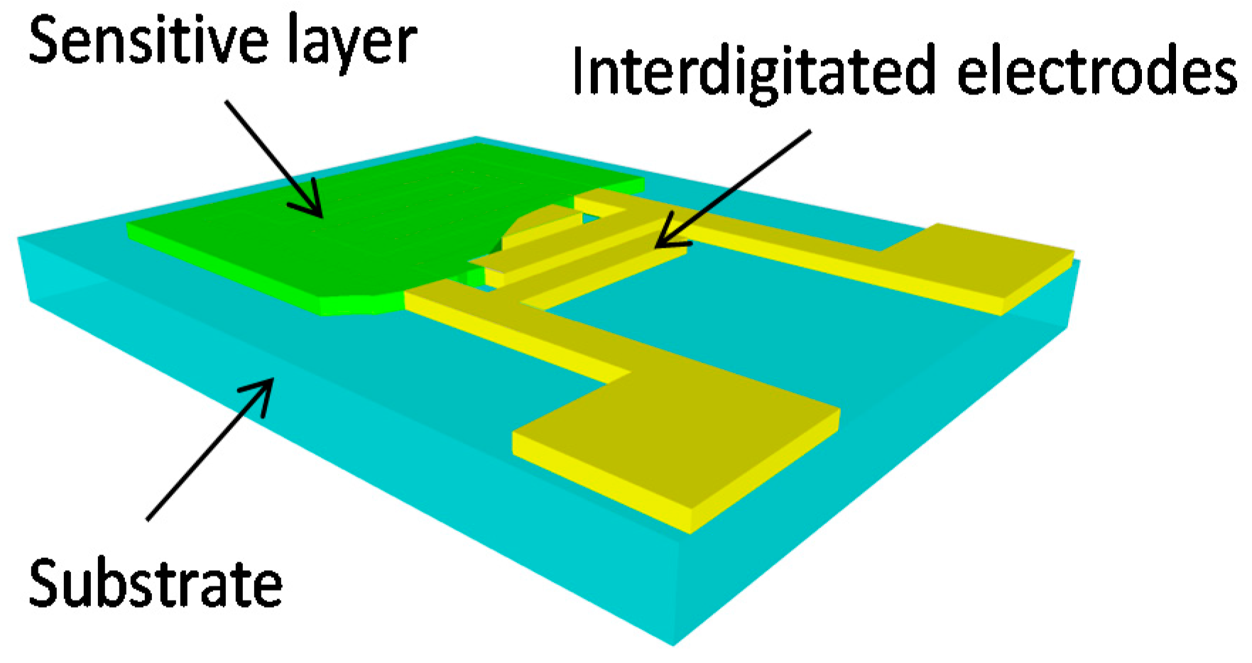
Abstract
:1. Introduction
2. Materials and Methods
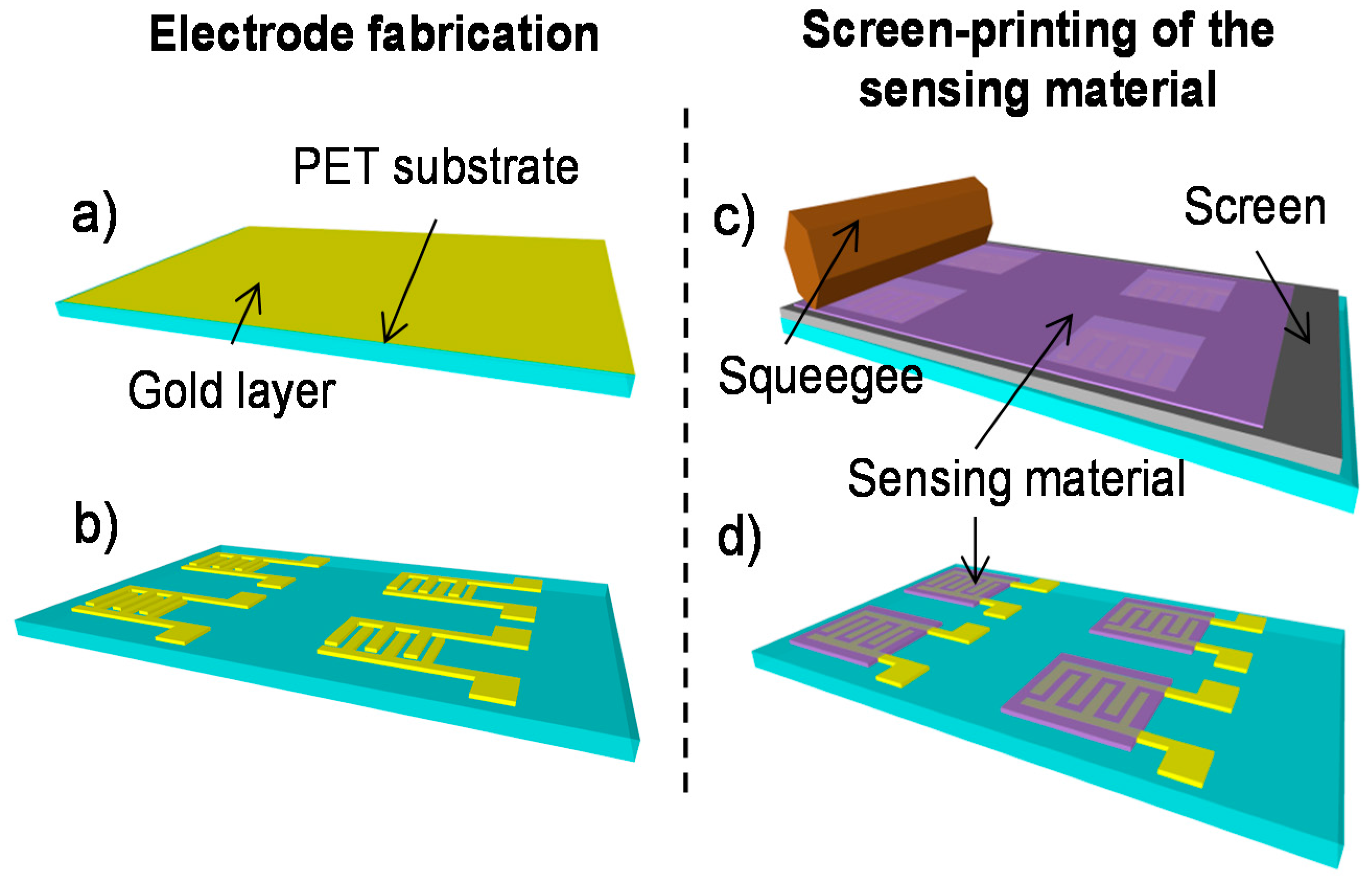
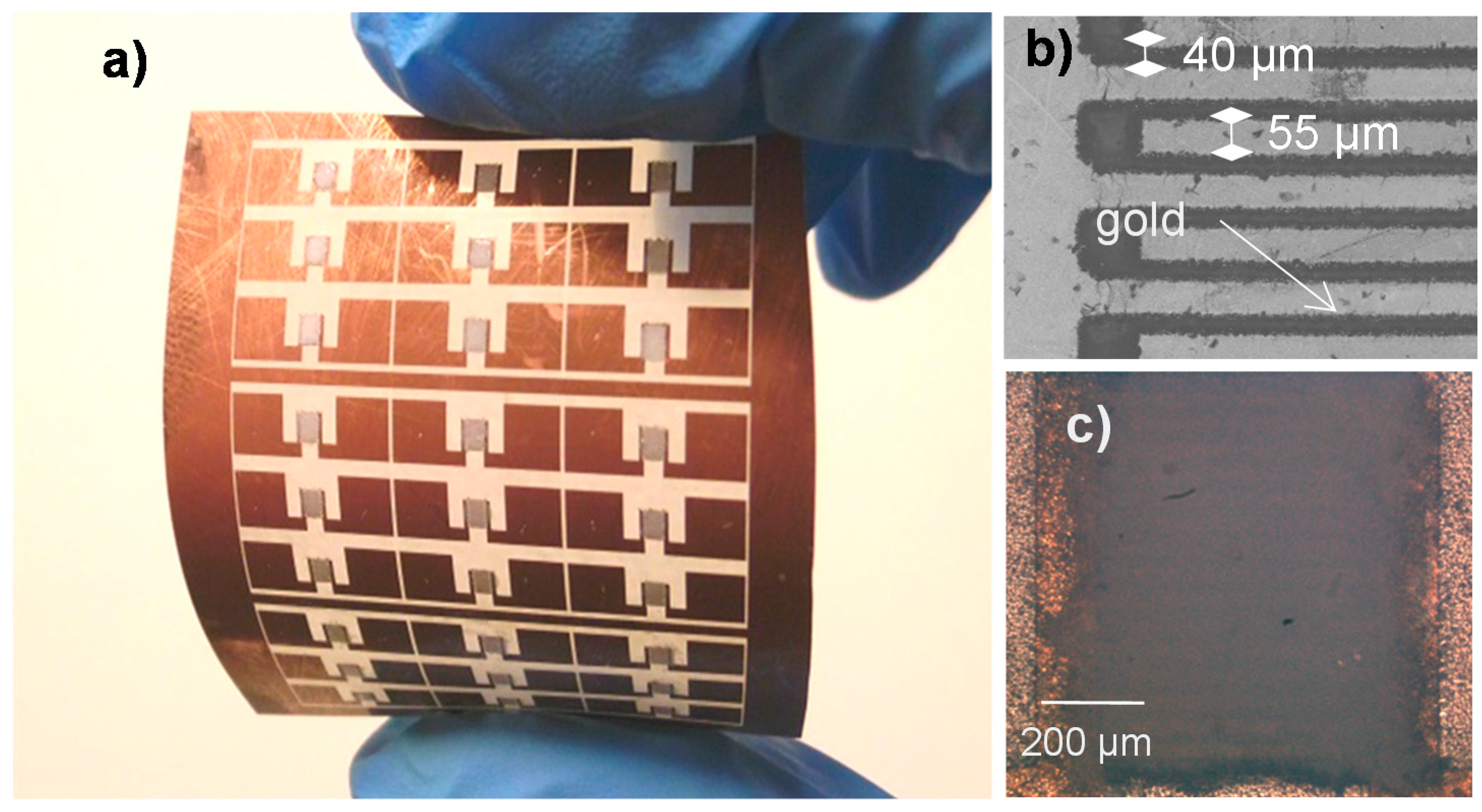
2.1. Fabrication
2.1.1. Laser Ablation of the Interdigitated Electrodes
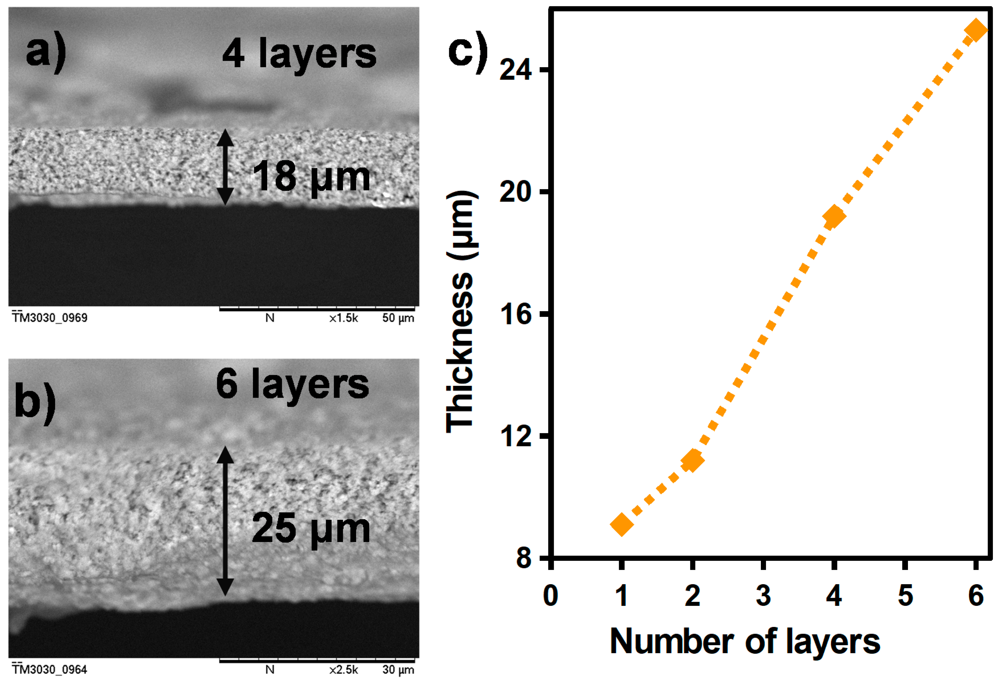
2.1.2. Sensitive Layer: Preparation and Screen-Printing
2.2. Measurements
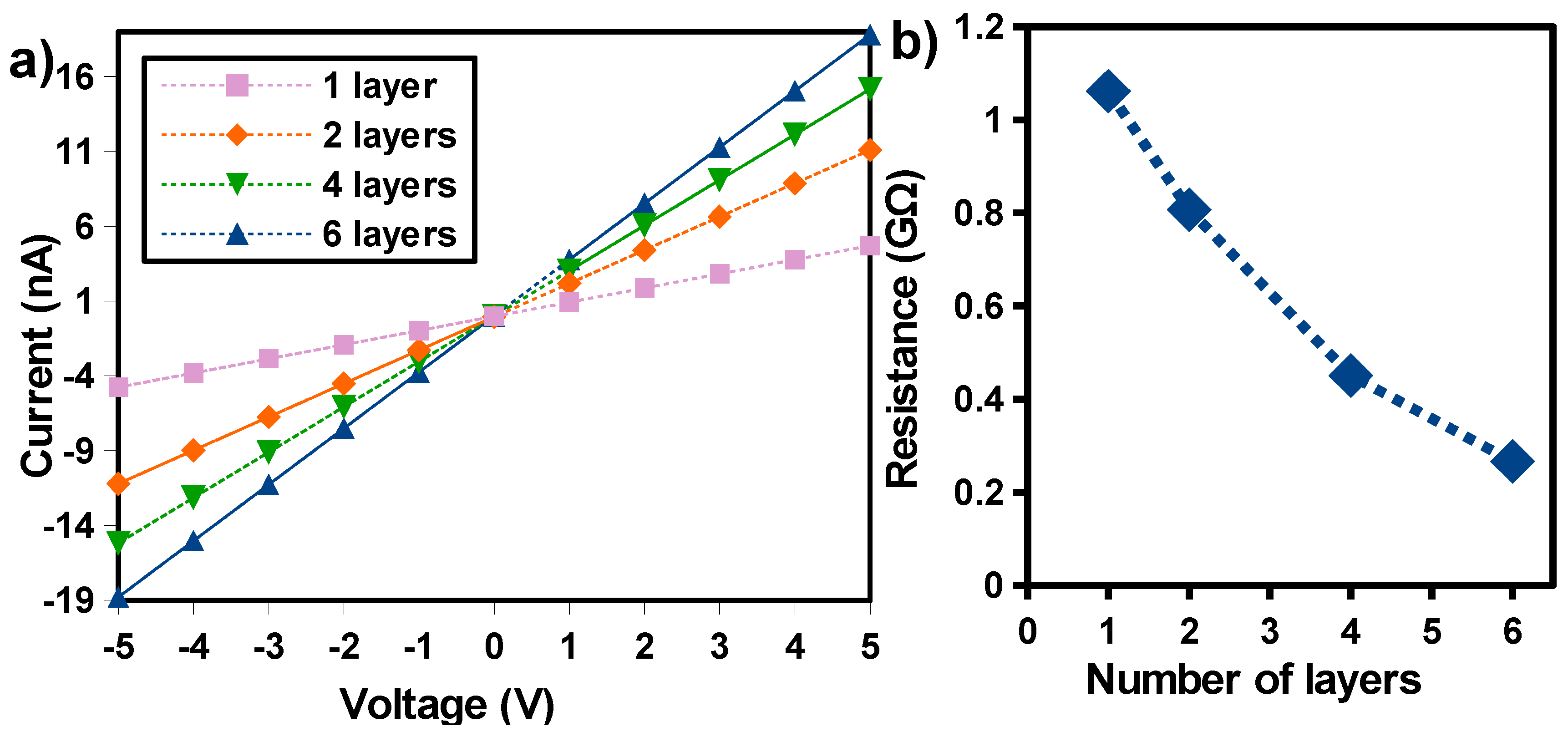
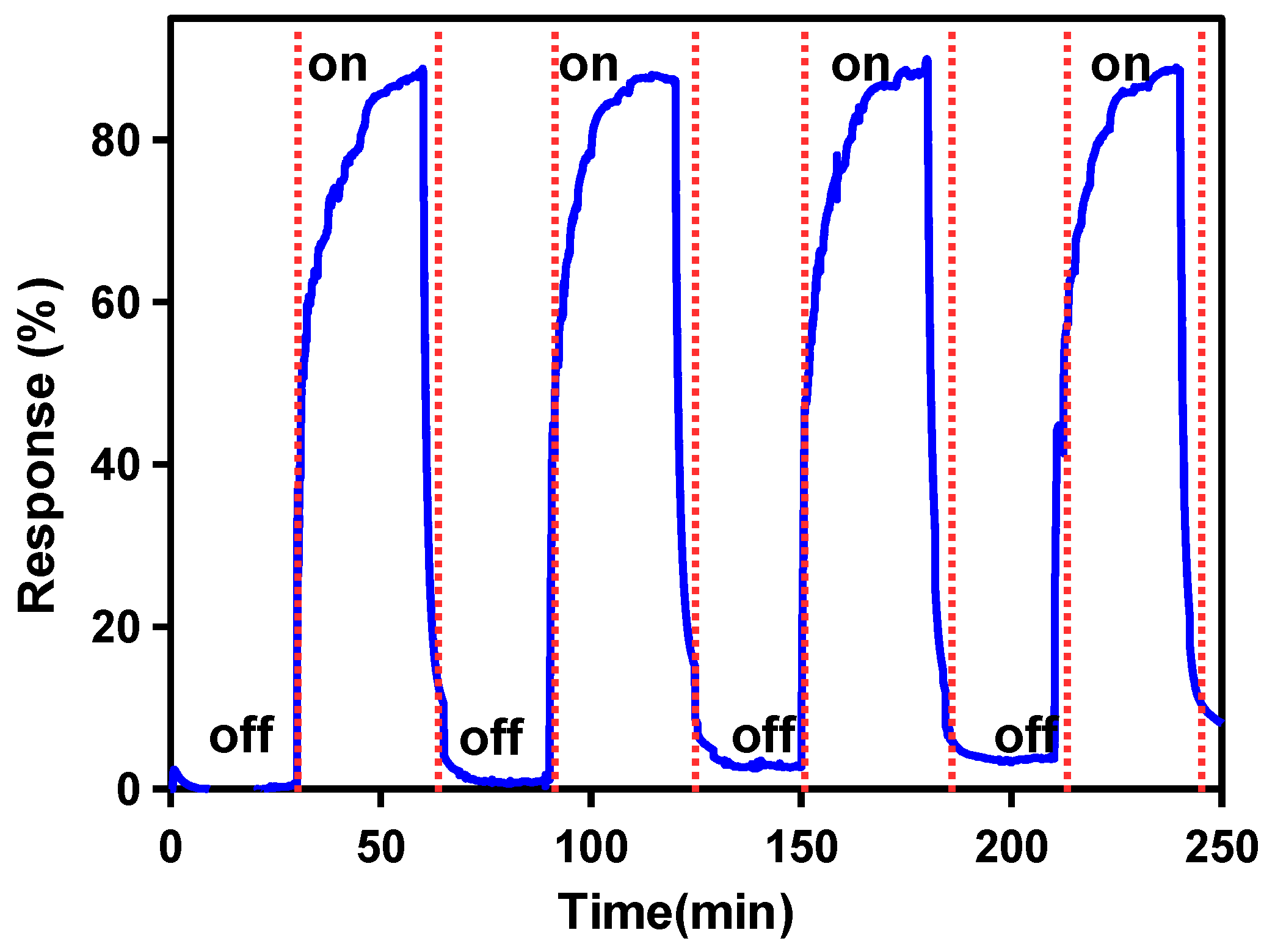
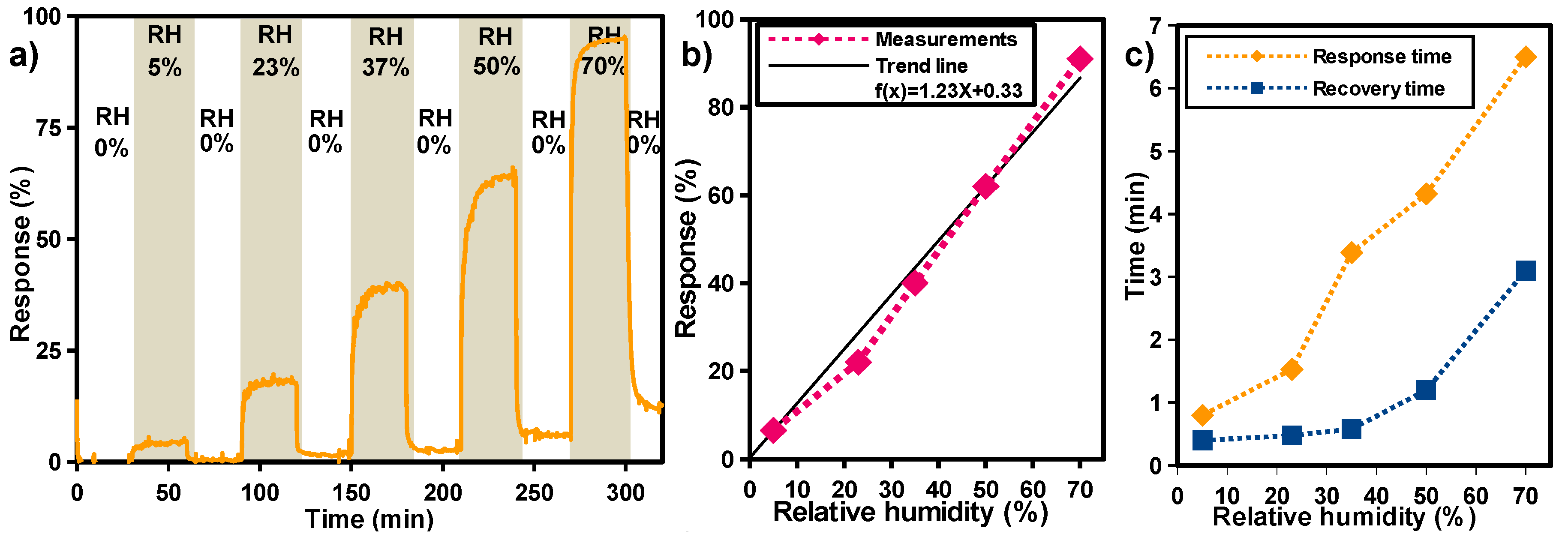
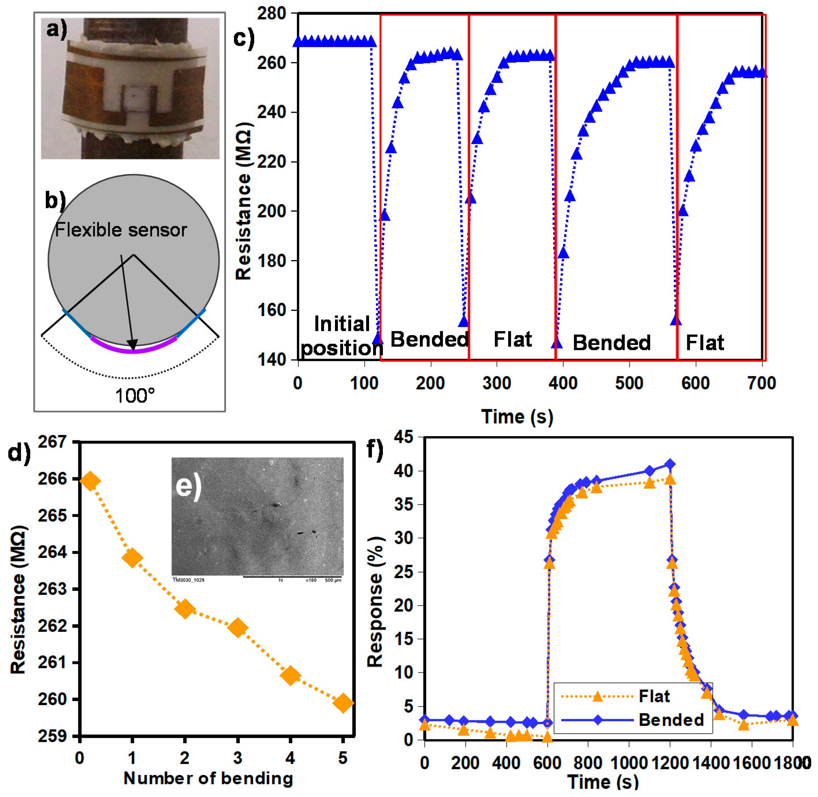
3. Results and Discussion
4. Conclusions
Acknowledgements
Author Contributions
Conflicts of Interest
References
- Zhang, Y.; Yu, K.; Jiang, D.; Zhu, Z.; Geng, H.; Luo, L. Zinc Oxide Nanorod and Nanowire for Humidity Sensor. Appl. Surf. Sci. 2005, 242, 212–217. [Google Scholar] [CrossRef]
- Arregui, F.J.; Liu, Y.; Matias, I.R.; Claus, R.O. Optical Fiber Humidity Sensor Using a Nano Fabry-Perot Cavity Formed by the Ionic Self-Assembly Method. Sens. Actuator B Chem. 1999, 59, 54–59. [Google Scholar] [CrossRef]
- Southworth, D.R.; Bellan, L.M.; Linzon, Y.; Craighead, H.G.; Parpia, J.M. Stress-based vapor sensing using resonant microbridges. Appl. Phys. Lett. 2010, 96, 163503. [Google Scholar] [CrossRef]
- Penza, M.; Anisimkin, V.I. Surface acoustic wave humidity sensor using polyvinyl-alcohol film. Sens. Actuator A Phys. 1999, 76, 162–166. [Google Scholar] [CrossRef]
- Someya, T.; Sekitani, T.; Iba, S.; Kato, Y.; Kawaguchi, H.; Sakurai, T. A large-area, flexible pressure sensor matrix with organic field-effect transistors for artificial skin applications. Proc. Natl. Acad. Sci. USA 2004, 101, 9966–9970. [Google Scholar] [CrossRef] [PubMed]
- Thuau, D.; Abbas, M.; Wantz, G.; Hirsch, L.; Dufour, I.; Ayelab, C. Piezoelectric polymer gated OFET: Cutting-edge electro-mechanical transducer for organic MEMS-based sensors. Sci. Rep. 2016, 6, 38672. [Google Scholar] [CrossRef] [PubMed]
- Molina-Lopez, F.; Quintero, A.V.; Mattana, G.; Briand, D.; de Rooij, N. Large-area compatible fabrication and encapsulation of inkjet-printed humidity sensors on flexible foils with integrated thermal compensation. J. Micromech. Microeng. 2013, 23, 025012. [Google Scholar] [CrossRef]
- Quddious, A.; Yang, S.; Khan, M.M.; Tahir, F.A.; Shamim, A.; Salama, K.N.; Cheema, H.M. Disposable, Paper-Based, Inkjet-Printed Humidity and H2S Gas Sensor for Passive Sensing Applications. Sensors 2016, 16, 2073. [Google Scholar] [CrossRef] [PubMed]
- Oprea, A.; Courbat, J.; Bârsan, N.; Briand, D.; de Rooij, N.F.; Weimar, U. Temperature, humidity and gas sensors integrated on plastic foil for low power applications. Sens. Actuators B Chem. 2009, 140, 227–232. [Google Scholar] [CrossRef]
- Deng, F.; He, Y.; Zhang, C.; Feng, W. A CMOS Humidity Sensor for Passive RFID Sensing Applications. Sensors 2014, 14, 8728–8739. [Google Scholar] [CrossRef] [PubMed]
- Presmanes, L.; Thimont, Y.; Chapelle, A.; Blanc, F.; Talhi, C.; Bonningue, C.; Barnabé, A.; Menini, P.H.; Tailhades, P.H. Highly Sensitive Sputtered ZnO:Ga Thin Films Integrated by a Simple Stencil Mask Process on Microsensor Platforms for Sub-ppm Acetaldehyde Detection. Sensors 2017, 17, 1055. [Google Scholar] [CrossRef] [PubMed]
- Moore, G.E. Cramming more components onto integrated circuits. Proc. IEEE 1998, 86, 82–85. [Google Scholar] [CrossRef]
- Zhao, P.; Deng, N.; Li, X.W.; Ren, C.C.; Wang, Z.Y. Development of highly-sensitive and ultra-thin silicon stress sensorchips for wearable biomedical applications. Sens. Actuators A Phys. 2014, 216, 158–166. [Google Scholar] [CrossRef]
- Kim, J.; Son, D.; Lee, M.; Song, C.; Song, J.K.; Koo, J.H.; Lee, D.J.; Shim, H.J.; Kim, J.H.; Lee, M.; et al. A wearable multiplexed silicon nonvolatile memory array using nanocrystal charge confinement. Sci. Adv. 2016, 2, e1501101. [Google Scholar] [CrossRef] [PubMed]
- Wang, X.; Larsson, O.; Platt, D.; Nordlinder, S.; Engquist, I.; Berggren, M.; Crispin, X. An all-printed wireless humidity sensor label. Sens. Actuators B Chem. 2012, 166–167, 556–561. [Google Scholar] [CrossRef]
- Salmerón, J.F.; Molina-Lopez, F.; Briand, D.; Ruan, J.J.; Rivadeneyra, A.; Carvajal, M.A.; Capitán-Vallvey, L.; de Rooij, N.F.; Palma, A.J. Properties and Printability of Inkjet and Screen-Printed Silver Patterns for RFID Antennas. J. Electron. Mater. 2014, 43, 604–617. [Google Scholar] [CrossRef]
- Lee, C.Y.; Wu, G.W.; Hsieh, W.J. Fabrication of micro sensors on a flexible substrate. Sens. Actuators A Phys. 2008, 147, 173–176. [Google Scholar] [CrossRef]
- Wang, L.; Luo, J.; Yin, J.; Zhang, H.; Wu, J.; Shi, X.; Crew, E.; Xu, Z.; Rendeng, Q.; Lu, S.; et al. Flexible chemiresistor sensors: Thin film assemblies of nanoparticles on a polyethylene terephthalate substrate. J. Mater. Chem. 2010, 20, 907–915. [Google Scholar] [CrossRef]
- Zampetti, E.; Maiolo, L.; Pecora, A.; Maita, F.; Pantalei, S.; Minotti, A.; Valletta, A.; Cuscunà, M.; Macagnano, A.; Fortunato, G.; et al. Flexible sensorial system based on capacitive chemical sensors integrated with readout circuits fully fabricated on ultra-thin substrate. Sens. Actuators B Chem. 2011, 155, 768–774. [Google Scholar] [CrossRef]
- Zampetti, E.; Pantalei, S.; Pecora, A.; Valletta, A.; Maiolo, L.; Minotti, A.; Macagnano, A.; Fortunato, G.; Bearzotti, A. Design and optimization of an ultra thin flexible capacitive humidity sensor. Sens. Actuators B Chem. 2009, 143, 302–307. [Google Scholar] [CrossRef]
- Acuautla, M.; Bernardini, S.; Gallais, L.; Florido, T.; Patout, L.; Bendahan, M. Ozone flexible sensors fabricated by photolithography and laser ablation processes based on ZnO nanoparticles. Sens. Actuators B Chem. 2014, 203, 602–611. [Google Scholar] [CrossRef]
- Fujishima, A.; Honda, K. Electrochemical Photolysis of Water at a Semiconductor Electrode. Nature 1972, 238, 37–38. [Google Scholar] [CrossRef] [PubMed]
- Grätzel, M. Photoelectrochemical cells. Nature 2001, 414, 338–344. [Google Scholar] [CrossRef] [PubMed]
- Konstantinou, I.K.; Albanis, T.A. TiO2-assisted photocatalytic degradation of azo dyes in aqueous solution: Kinetic and mechanistic investigations: A review. Appl. Catal. B Environ. 2004, 49, 1–41. [Google Scholar] [CrossRef]
- Ni, M.; Leung, M.K.H.; Leung, D.Y.C.; Sumathy, K. A review and recent developments in photocatalytic water-splitting using TiO2 for hydrogen production. Renew. Sustain. Energy Rev. 2007, 11, 401–425. [Google Scholar] [CrossRef]
- Millis, A.; Hunte, S.L. An overview of semiconductor photocatalysis. J. Photochem. Photobiol. A Chem. 1997, 108, 1–35. [Google Scholar] [CrossRef]
- Dennis, J.O.; Ahmed, A.Y.; Khir, M.H. Fabrication and characterization of a CMOS-MEMS humidity sensor. Sensor 2015, 15, 16674–16687. [Google Scholar] [CrossRef] [PubMed]
- Ghadiry, M.; Gholami, M.; Kong, L.C.; Yi, C.W.; Ahmad, H.; Alias, Y. Nano-Anatase TiO2 for High Performance Optical Humidity Sensing on Chip. Sensors 2016, 16, 39. [Google Scholar] [CrossRef] [PubMed]
- Montesperelli, G.; Pumo, A.; Traversa, E.; Bearzotti, A.; Montenero, A.; Gnappi, G. Sol-Gel Processed TiO2-Based Thin Films as Innovative Humidity Sensors. Sens. Actuators B Chem. 1995, 25, 705–709. [Google Scholar] [CrossRef]
- Wang, Z.; Shi, L.; Wu, F.; Yuan, S.; Zhao, Y.; Zhang, M. The sol-gel template synthesis of porous TiO2 for a high performance humidity sensor. Nanotechnology 2011, 22, 275502. [Google Scholar] [CrossRef] [PubMed]
- Hu, Y.C.; Dai, C.L.; Hsu, C.C. Titanium Dioxide Nanoparticle Humidity Microsensors Integrated with Circuitry on-a-Chip. Sensors 2014, 14, 4177–4188. [Google Scholar] [CrossRef] [PubMed] [Green Version]
- Zhang, G.; Wu, Y.; Fu, P.; Wang, G.; Pan, S.; Chen, C. Nanocrystalline TiO2 Electrodes Prepared by Water-Medium Screen Printing Technique. Chem. Lett. 2001, 30, 1042–1043. [Google Scholar]
- Ito, S.; Chen, P.; Comte, P.; Nazeeruddin, M.K.; Liska, P.; Pechy, P.; Gratzel, M. Fabrication of Screen-Printing Pastes from TiO2 Powders for Dye-Sensitised Solar Cells. Prog. Photovolt. 2007, 15, 603–612. [Google Scholar] [CrossRef]
- Meijer, J.; Du, K.; Gillner, A.; Hoffmann, D.; Kovalenko, V.S.; Masuzawa, T.; Ostendorf, A.; Poprawe, R.; Schulz, W. Laser machining by short and ultrashort pulses, state of the art and new opportunities in the age of the photons. CIRP Ann. Manuf. Technol. 2002, 51, 531–550. [Google Scholar] [CrossRef]
- Dubourg, G.; Zlebic, C.; Matovic, J.; Bengin, V.C. One-step patterning of a flexible piezoresistive MEMS sensor by 3D direct laser writing. In Proceedings of the 2015 IEEE 10th International Conference on Nano/Micro Engineered and Molecular Systems (NEMS), Xi’an, China, 7–11 April 2015; pp. 553–556. [Google Scholar]
- Niarchos, G.; Dubourg, G.; Afroudakis, G.; Georgopoulos, M.; Tsouti, V.; Makarona, E.; Crnojevic-Bengin, V.; Tsamis, C. Humidity sensing properties of paper substrates and their passivation with ZnO nanoparticles for sensor applications. Sensors 2017, 17, 516. [Google Scholar] [CrossRef] [PubMed]
- Cao, X.; Chen, H.; Gu, X.; Liu, B.; Wang, W.; Cao, Y.; Wu, F.; Zhou, C. Screen Printing as a Scalable and Low-Cost Approach for Rigid and Flexible Thin-Film Transistors Using Separated Carbon Nanotubes. ACS Nano 2014, 8, 12769–12776. [Google Scholar] [CrossRef] [PubMed]
- Li, M.; Li, Y.-T.; Li, D.-W.; Long, Y.-T. Recent developments and applications of screen-printed electrodes in environmental assays—A review. Anal. Chim. Acta 2012, 734, 31–44. [Google Scholar] [CrossRef] [PubMed]
- Bai, J.; Zhou, B. Titanium dioxide nanomaterials for sensor applications. Chem. Rev. 2014, 114, 10131–10176. [Google Scholar] [CrossRef] [PubMed]
- Yang, T.; Yu, Y.Z.; Zhu, L.S.; Wu, X.; Wang, X.H.; Zhang, J. Fabrication of silver interdigitated electrodes on polyimide films via surface modification and ion-exchange technique and its flexible humidity sensor application. Sens. Actuators B Chem. 2015, 208, 327–333. [Google Scholar] [CrossRef]
- Xuan, W.; He, X.; Chen, J.; Wang, W.; Wang, X.; Xu, Y.; Xu, Z.; Fu, Y.Q.; Luo, J. High sensitivity flexible lamb-wave humidity sensors with a graphene oxide sensing layer. Nanoscale 2015, 7, 7430–7436. [Google Scholar] [CrossRef] [PubMed]
- Nakajima, T.; Nakamura, T.; Tsuchiya, T. Flexible humidity sensors composed of graphite-like carbon micro-pinecone arrays. RSC Adv. 2016, 6, 95342–95348. [Google Scholar] [CrossRef]
- Li, W.; Xu, F.; Sun, L.; Liu, W.; Qiu, Y. A novel flexible humidity switch material based on multi-walled carbon nanotube/polyvinyl alcohol composite yarn. Sens. Actuators B 2016, 230, 528–535. [Google Scholar] [CrossRef]


© 2017 by the authors. Licensee MDPI, Basel, Switzerland. This article is an open access article distributed under the terms and conditions of the Creative Commons Attribution (CC BY) license (http://creativecommons.org/licenses/by/4.0/).
Share and Cite
Dubourg, G.; Segkos, A.; Katona, J.; Radović, M.; Savić, S.; Niarchos, G.; Tsamis, C.; Crnojević-Bengin, V. Fabrication and Characterization of Flexible and Miniaturized Humidity Sensors Using Screen-Printed TiO2 Nanoparticles as Sensitive Layer. Sensors 2017, 17, 1854. https://doi.org/10.3390/s17081854
Dubourg G, Segkos A, Katona J, Radović M, Savić S, Niarchos G, Tsamis C, Crnojević-Bengin V. Fabrication and Characterization of Flexible and Miniaturized Humidity Sensors Using Screen-Printed TiO2 Nanoparticles as Sensitive Layer. Sensors. 2017; 17(8):1854. https://doi.org/10.3390/s17081854
Chicago/Turabian StyleDubourg, Georges, Apostolos Segkos, Jaroslav Katona, Marko Radović, Slavica Savić, Georgios Niarchos, Christos Tsamis, and Vesna Crnojević-Bengin. 2017. "Fabrication and Characterization of Flexible and Miniaturized Humidity Sensors Using Screen-Printed TiO2 Nanoparticles as Sensitive Layer" Sensors 17, no. 8: 1854. https://doi.org/10.3390/s17081854