
Implications for a Wireless, External Device System to Study Electrocorticography

 ,
,
Abstract
:1. Introduction
2. Results
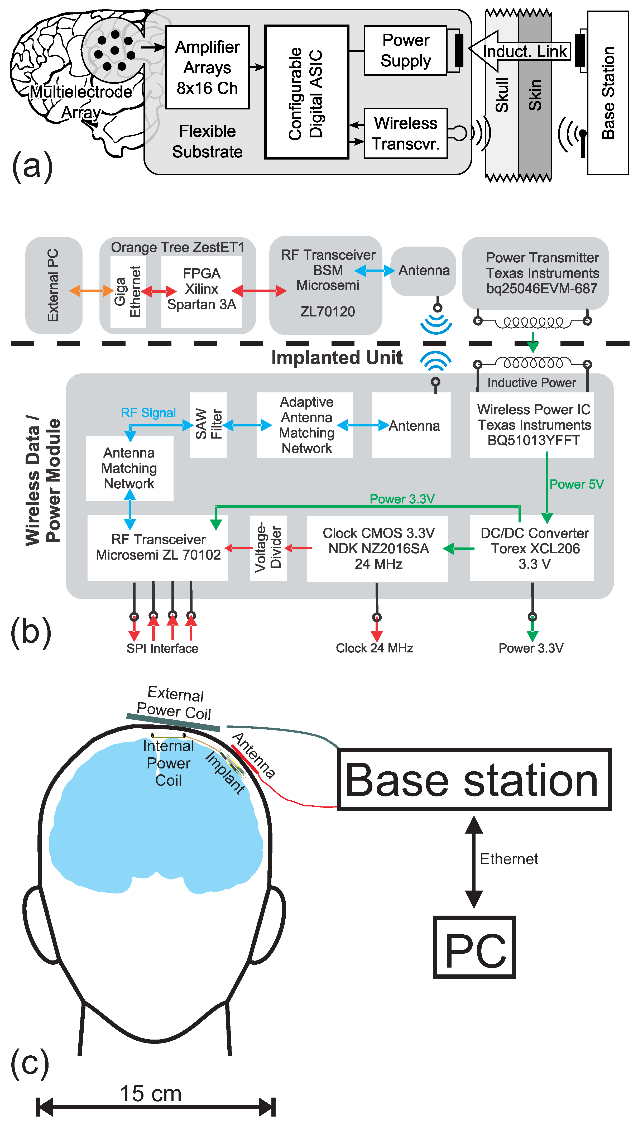
2.1. System Concept
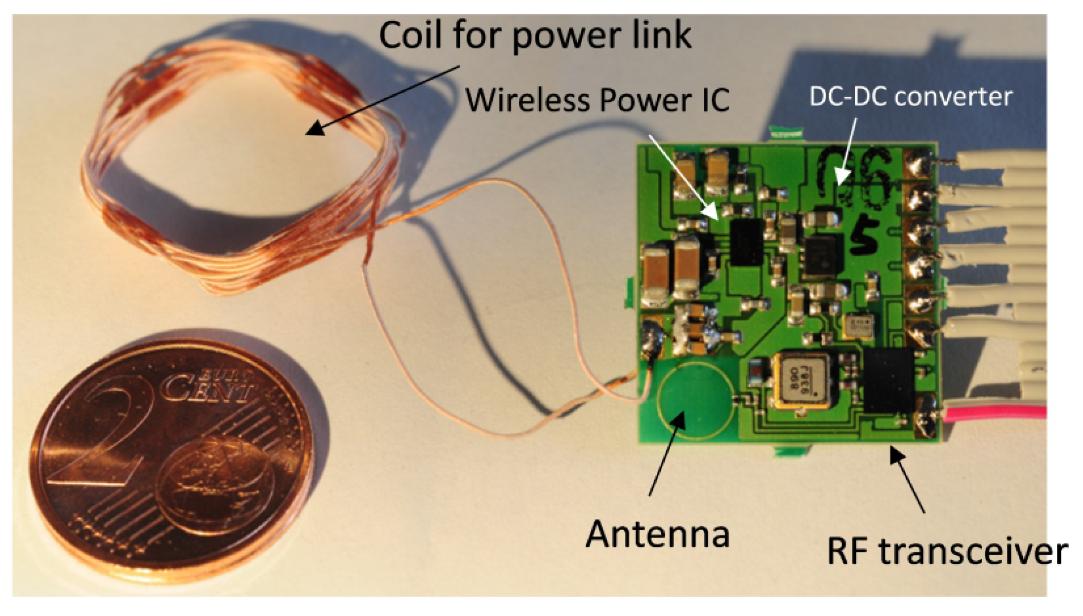
2.2. The Wireless Module
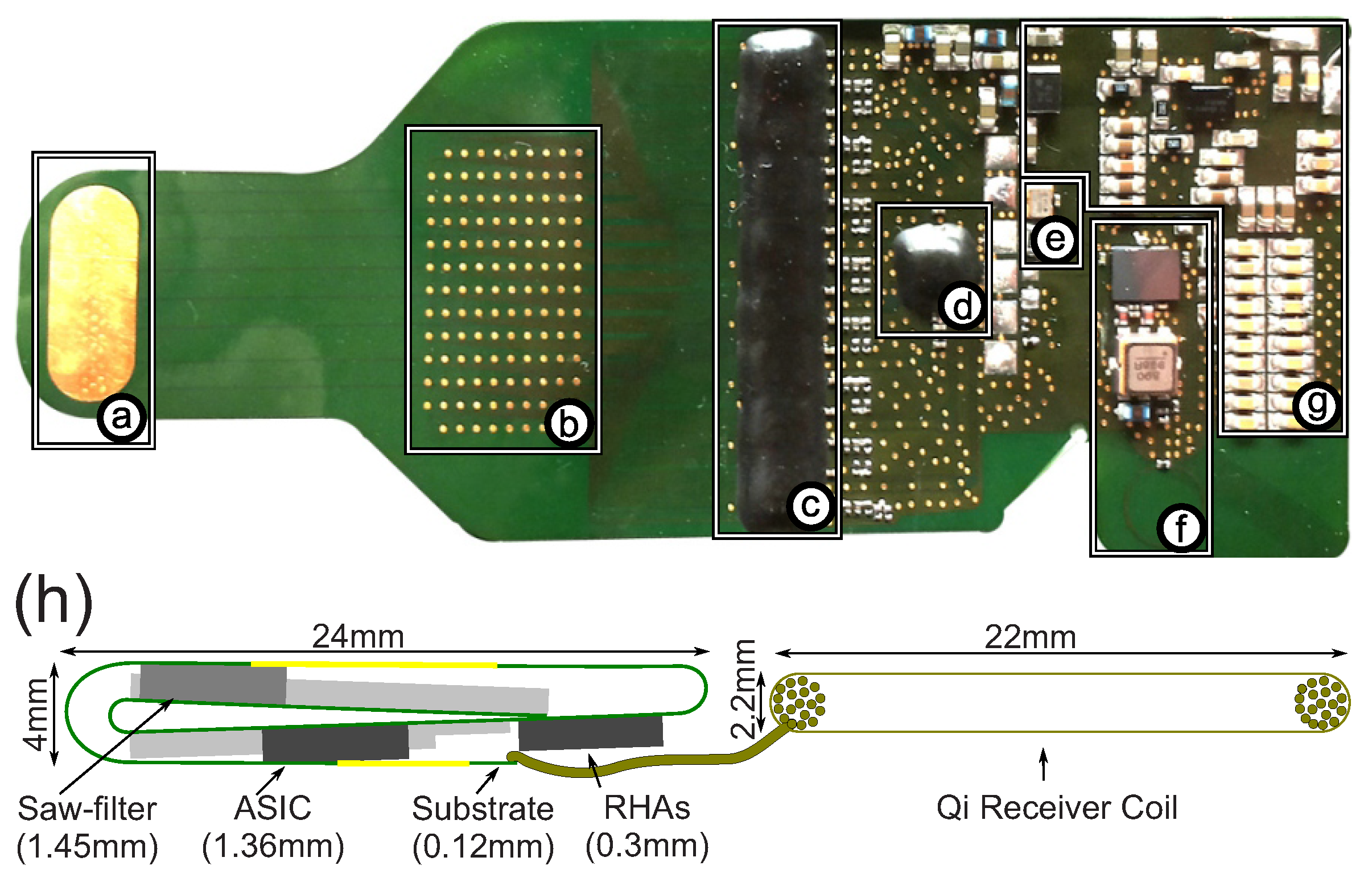
2.3. The Implant Prototype
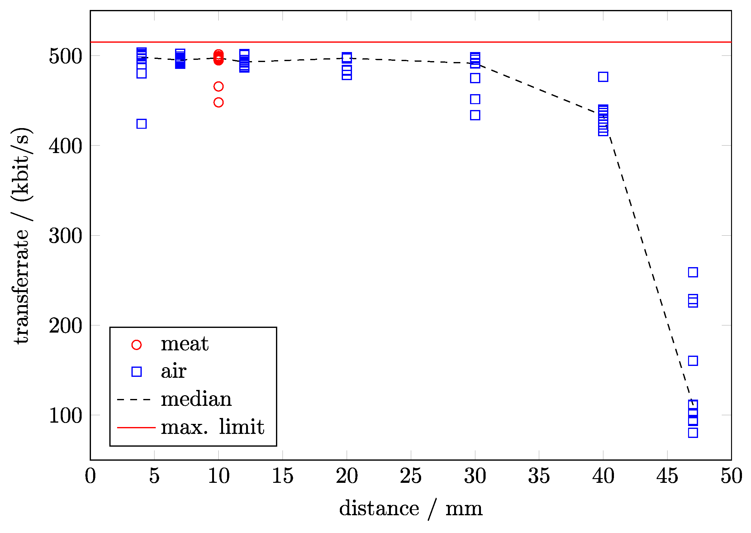
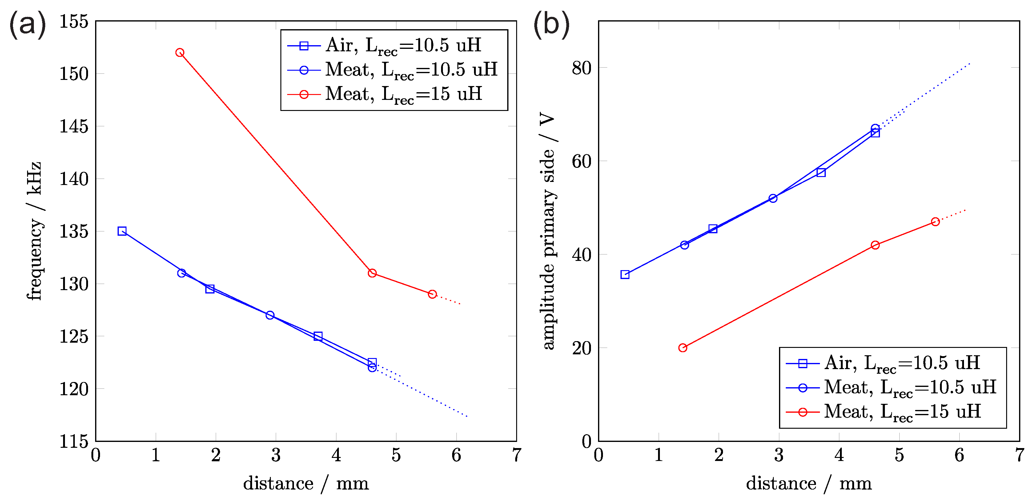
2.4. Performance of the Wireless Module
2.5. Performance of the Analog Front End
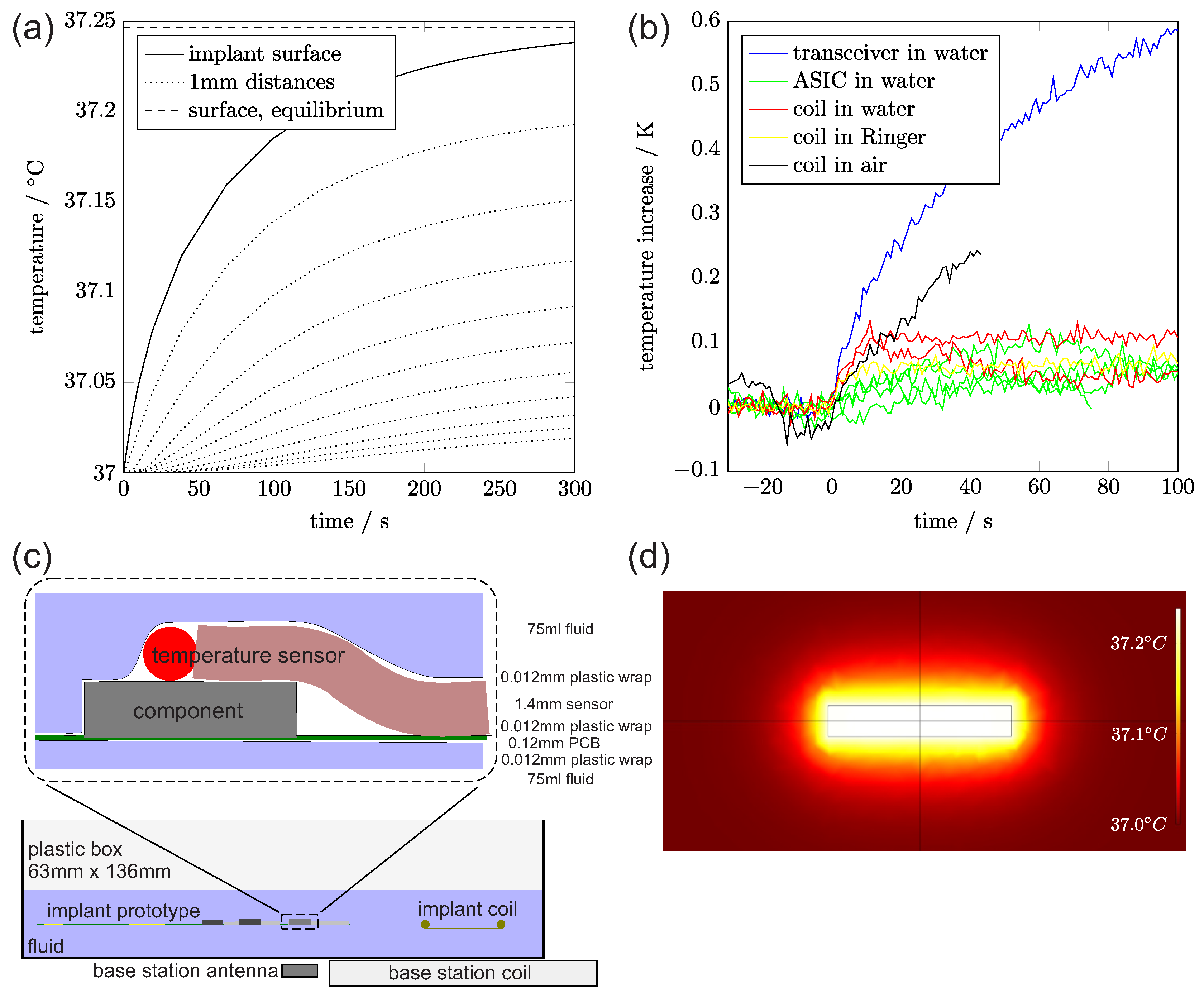
2.6. Examining the Implant’s Thermal Properties
3. Discussion
Supplementary Materials
Acknowledgments
Author Contributions
Conflicts of Interest
References
- Lebedev, M.; Tate, A.; Hanson, T.; Li, Z.; O’Doherty, J.; Winans, J.; Ifft, P.; Zhuang, K.; Fitzsimmons, N.; Schwarz, D.; et al. Future developments in brain-machine interface research. Clinics (Sao Paulo) 2011, 66, 25–32. [Google Scholar] [CrossRef] [PubMed]
- Van Gerven, M.; Farquhar, J.; Schaefer, R.; Vlek, R.; Geuze, J.; Nijholt, A.; Ramsey, N.; Haselager, P.; Vuurpijl, L.; Gielen, S.; et al. The brain–computer interface cycle. J. Neural Eng. 2009, 6, 041001. [Google Scholar] [CrossRef] [PubMed]
- Lebedev, M.; Nicolelis, M. Brain-machine interfaces: Past, present and future. Trends Neurosci. 2006, 29, 536–546. [Google Scholar] [CrossRef] [PubMed]
- Andersen, R.; Hwang, E.; Mulliken, G. Cognitive Neural Prosthetics. Annu. Rev. Psychol. 2010, 61, 169–190. [Google Scholar] [CrossRef] [PubMed]
- Velliste, M.; Perel, S.; Spalding, M.; Whitford, A.; Schwartz, A. Cortical control of a prosthetic arm for self-feeding. Nature 2008, 453, 1098–1101. [Google Scholar] [CrossRef] [PubMed]
- Wang, W.; Collinger, J.L.; Degenhart, A.D.; Tyler-Kabara, E.C.; Schwartz, A.B.; Moran, D.W.; Weber, D.J.; Wodlinger, B.; Vinjamuri, R.K.; Ashmore, R.C.; et al. An electrocorticographic brain interface in an individual with tetraplegia. PLoS ONE 2013, 8, e55344. [Google Scholar] [CrossRef] [PubMed]
- Hochberg, L.; Serruya, M.; Friehs, G.; Mukand, J.; Saleh, M.; Caplan, A.; Branner, A.; Chen, D.; Penn, R.; Donoghue, J. Neuronal ensemble control of prosthetic devices by a human with tetraplegia. Nature 2006, 442, 164–171. [Google Scholar] [CrossRef] [PubMed]
- Musallam, S.; Corneil, B.; Greger, B.; Scherberger, H.; Andersen, R. Cognitive Control Signals for Neural Prosthetics. Science 2004, 305, 258–262. [Google Scholar] [CrossRef] [PubMed]
- Moran, D. Evolution of brain–computer interface: Action potentials, local field potentials and electrocorticograms. Curr. Opin. Neurobiol. 2010, 20, 741–745. [Google Scholar] [CrossRef] [PubMed]
- Jarosiewicz, B.; Sarma, A.A.; Bacher, D.; Masse, N.Y.; Simeral, J.D.; Sorice, B.; Oakley, E.M.; Blabe, C.; Pandarinath, C.; Gilja, V.; et al. Virtual typing by people with tetraplegia using a self-calibrating intracortical brain-computer interface. Sci. Transl. Med. 2015, 7, 313ra179. [Google Scholar] [CrossRef] [PubMed]
- Schalk, G. Can Electrocorticography (ECoG) Support Robust and Powerful Brain–Computer Interfaces? Front. Neuroeng. 2010, 3, 9. [Google Scholar] [CrossRef] [PubMed]
- Silay, K.M.; Dehollain, C.; Declercq, M. Numerical analysis of temperature elevation in the head due to power dissipation in a cortical implant. In Proceedings of the 30th Annual International Conference of the IEEE, Engineering in Medicine and Biology Society, Vancouver, BC, Canada, 20–25 August 2008. [Google Scholar]
- Kim, S.; Tathireddy, P.; Normann, R.A.; Solzbacher, F. In vitro and in vivo study of temperature increases in the brain due to a neural implant. In Proceedings of the 3rd International IEEE/EMBS Conference on Neural Engineering, Kohala Coast, HI, USA, 2–5 May 2007. [Google Scholar]
- Kim, S.; Tathireddy, P.; Normann, R.A.; Solzbacher, F. Thermal Impact of an Active 3-D Microelectrode Array Implanted in the Brain. IEEE Trans. Neural Syst. Rehabil. Eng. 2007, 15, 493–501. [Google Scholar] [PubMed]
- Voges, J.; Waerzeggers, Y.; Maarouf, M.; Lehrke, R.; Koulousakis, A.; Lenartz, D.; Sturm, V. Deep-brain stimulation: Long-term analysis of complications caused by hardware and surgery—Experiences from a single centre. J. Neurol. Neurosurg. Psychiatry 2006, 77, 868–872. [Google Scholar] [CrossRef] [PubMed]
- Lee, W.S.; Lee, J.K.; Lee, S.A.; Kang, J.K.; Ko, T.S. Complications and results of subdural grid electrode implantation in epilepsy surgery. Surg. Neurol. 2000, 54, 346–351. [Google Scholar] [CrossRef]
- Nair, D.R.; Burgess, R.; McIntyre, C.C.; Lueders, H. Chronic subdural electrodes in the management of epilepsy. Clin. Neurophysiol. 2008, 119, 11–28. [Google Scholar] [CrossRef] [PubMed]
- Ahn, D.; Ghovanloo, M. Optimal design of wireless power transmission links for millimeter-sized biomedical implants. IEEE Trans. Biomed. Circuits Syst. 2016, 10, 125–137. [Google Scholar] [CrossRef] [PubMed]
- Bahrami, H.; Mirbozorgi, S.A.; Ameli, R.; Rusch, L.A.; Gosselin, B. Flexible, polarization-diverse UWB antennas for implantable neural recording systems. IEEE Trans. Biomed. Circuits Syst. 2016, 10, 38–48. [Google Scholar] [CrossRef] [PubMed]
- Borton, D.A.; Yin, M.; Aceros, J.; Nurmikko, A. An implantable wireless neural interface for recording cortical circuit dynamics in moving primates. J. Neural Eng. 2013, 10, 026010. [Google Scholar] [CrossRef] [PubMed]
- Muller, R.; Hanh-Phuc, L.; Wen, L.; Ledochowitsch, P.; Gambini, S.; Bjorninen, T.; Koralek, A.; Carmena, J.; Maharbiz, M.; Alon, E.; et al. 24.1 A miniaturized 64-channel 225 μW wireless electrocorticographic neural sensor. In Proceedings of the Solid-State Circuits Conference Digest of Technical Papers (ISSCC), San Francisco, CA, USA, 9–13 February 2014. [Google Scholar]
- Hirata, M.; Matsushita, K.; Suzuki, T.; Yoshida, T.; Sato, F.; Morris, S.; Yanagisawa, T.; Goto, T.; Kawato, M.; Yoshimine, T. A Fully-Implantable Wireless System for Human Brain-Machine Interfaces Using Brain Surface Electrodes: W-HERBS. IEICE Trans. Commun. 2011, E94-B, 2448–2453. [Google Scholar] [CrossRef]
- Aceros, J.; Yin, M.; Borton, D.; Patterson, W.; Nurmikko, A. A 32-channel fully implantable wireless neurosensor for simultaneous recording from two cortical regions. In Proceedings of the Annual International Conference of the IEEE Engineering in Medicine and Biology Society, Boston, MA, USA, 30 August–3 September 2011; pp. 2300–2306. [Google Scholar]
- Chae, M.S.; Yang, Z.; Yuce, M.R.; Hoang, L.; Liu, W. A 128-channel 6 mW wireless neural recording IC with spike feature extraction and UWB transmitter. IEEE Trans. Neural Syst. Rehabil. Eng. 2009, 17, 312–321. [Google Scholar] [CrossRef] [PubMed]
- Harrison, R.R.; Kier, R.J.; Kim, S.; Rieth, L.; Warren, D.J.; Ledbetter, N.M.; Clark, G.A.; Solzbacher, F.; Chestek, C.A.; Gilja, V.; et al. 100-Channel wireless neural recording system with 54-Mb/s data link and 40%-efficiency power link. In Proceedings of the 2012 IEEE Asian Solid State Circuits Conference (A-SSCC), Kobe, Japan, 12–14 November 2012; pp. 185–188. [Google Scholar]
- Wise, K.D. Wireless integrated microsystems: Wearable and implantable devices for improved health care. In Proceedings of the 2009 International Solid-State Sensors, Actuators and Microsystems Conference (TRANSDUCERS 2009), Denver, CO, USA, 21–25 June 2009; pp. 1–8. [Google Scholar]
- Zhang, F.; Holleman, J.; Otis, B.P. Design of ultra-low power biopotential amplifiers for biosignal acquisition applications. IEEE Trans. Biomed. Circuits Syst. 2012, 6, 344–355. [Google Scholar] [CrossRef] [PubMed]
- TI. bqTESLA Portfolio of Wireless Power Solutions, Texas Instruments: Dallas, TX, USA, 2011.
- TI. bq25046EVM-687 Evaluation Module, SLVU420; Texas Instruments: Dallas, TX, USA, 2010.
- TI. bq51013-Integrated Wireless Power Supply Receiver, Qi (Wireless Power Consortium) Compliant, SLVSAT9D; Texas Instruments: Dallas, TX, USA, 2012.
- Torex. XCL206-Inductor Built-In Step-Down Micro DC/DC Converters, Torex: Guadalajara, Mexico, 2011.
- Microsemi. ZL70102-Medical Implantable RF Transceiver MICS RF Telemetry, Microsemi: Aliso Viejo, CA, USA, 2010.
- Nihon Dempa Kogyo Co., Ltd. (NDK). NZ2016S Series—Crystal Clock Oscillator, NDK: Tokyo, Japan, 2013.
- RF Monolithics. RF2607D-403.5 MHz SAW Filter, RF Monolithics, Inc.: Dallas, TX, USA, 2010.
- Microsemi. ZL70120 MICS-Band RF Base Station Module (BSM), Rev. 4; Microsemi: Aliso Viejo, CA, USA, 2013.
- OrangeTreeTechnologies. ZestET1: GigE TOE & FPGA Module, Orange Tree Technologies: Oxfordshire, UK, 2013.
- Pistor, J.; Hoeffmann, J.; Rotermund, D.; Tolstosheeva, E.; Schellenberg, T.; Boll, D.; Gordillo-Gonzalez, V.; Mandon, S.; Peters-Drolshagen, D.; Kreiter, A.K.; et al. Development of a fully implantable recording system for ECoG signals. In Proceedings of the Conference on Design, Automation and Test in Europe, Grenoble, France, 18–22 March 2013. [Google Scholar]
- WPC—Wireless Power Consortium. WPC to Demo Worlds Most Advanced Resonant Wireless Charging System Compatible with Existing 40+ Million Qi Phones. 2014. Available online: https://www.wirelesspowerconsortium.com/data/downloadables/1/2/1/4/20140106-wpc-demonstrates-advanced-resonant-wireless-charging-system-at-ces.pdf (accessed on 3 April 2017).
- IEEE. IEEE Standard for Safety Levels with Respect to Human Exposure to Radio Frequency Electromagnetic Fields, 3 kHz to 300 GHz. 2006, p. 98. Available online: http://ieeexplore.ieee.org/document/1626482/ (accessed on 3 April 2017).
- Tolstosheeva, E.; Hoeffmann, J.; Pistor, J.; Rotermund, D.; Schellenberg, T.; Boll, D.; Hertzberg, T.; Gordillo-Gonzalez, V.; Mandon, S.; Peters-Drolshagen, D.; et al. Towards a Wireless and fully-implantable ECoG System. In Proceedings of the Transducers—The 17th International Conference on Solid-State Sensors, Actuators and Microsystems, Barcelona, Spain, 16–20 June 2013. [Google Scholar]


| Resource | Usage (RHA) | Usage (RHD) |
|---|---|---|
| CORE | 5859 of 6144 (95%) | 5236 of 6144 (85%) |
| IO (W/clocks) | 38 of 68 (56%) | 38 of 68 (56%) |
| GLOBAL (Chip + Quadrant) | 6 of 18 (33%) | 6 of 18 (33%) |
| PLL | 0 of 1 (0%) | 0 of 1 (0%) |
| RAM/FIFO | 8 of 8 (100%) | 8 of 8 (100%) |
| Component | Power Consumption |
|---|---|
| Microsemi ZL70102 transceiver | 17 mW (measured) |
| ASIC (Application-specific integrated circuit) | up to 9.44 mW (measured) |
| Clock quartz | 16.5 mW (measured) |
| Intan RHA amplifier arrays | 5 mW (each IC) (measured) |
| DC (direct current)/DC-Converter | 8.5 mW (for 1 RHA), 15 mW (for 8 RHAs), (data-sheet) |
| Texas Instruments inductive power receiver | 10–40 mW (data-sheet) |
© 2017 by the authors. Licensee MDPI, Basel, Switzerland. This article is an open access article distributed under the terms and conditions of the Creative Commons Attribution (CC BY) license (http://creativecommons.org/licenses/by/4.0/).
Share and Cite
Rotermund, D.; Pistor, J.; Hoeffmann, J.; Schellenberg, T.; Boll, D.; Tolstosheeva, E.; Gauck, D.; Stemmann, H.; Peters-Drolshagen, D.; Kreiter, A.K.; et al. Implications for a Wireless, External Device System to Study Electrocorticography. Sensors 2017, 17, 761. https://doi.org/10.3390/s17040761
Rotermund D, Pistor J, Hoeffmann J, Schellenberg T, Boll D, Tolstosheeva E, Gauck D, Stemmann H, Peters-Drolshagen D, Kreiter AK, et al. Implications for a Wireless, External Device System to Study Electrocorticography. Sensors. 2017; 17(4):761. https://doi.org/10.3390/s17040761
Chicago/Turabian StyleRotermund, David, Jonas Pistor, Janpeter Hoeffmann, Tim Schellenberg, Dmitriy Boll, Elena Tolstosheeva, Dieter Gauck, Heiko Stemmann, Dagmar Peters-Drolshagen, Andreas Kurt Kreiter, and et al. 2017. "Implications for a Wireless, External Device System to Study Electrocorticography" Sensors 17, no. 4: 761. https://doi.org/10.3390/s17040761