1. Introduction
With the ever-increasing demand for eco-design, environmental legislation for electronics is focused on two major requirements. One is the internationalization of the restriction of hazardous substances and the waste of electrical and electronic equipment; the other is a new directive especially for energy using products and the registration, evaluation, authorization, and restriction of chemicals [
1]. Lifetime extension is an important eco-design strategy for mitigating the environmental burden of developing new devices. Organic semiconductors increase the lifetime of large-area, low-cost image sensors by several thousand hours, and they monolithically integrate with photonic microsystems [
2]. Miniaturized power supply units tend to have a smaller environmental impact at the production stage than traditional electronics do [
1]; integrated circuitry can miniaturize power supplies. Colace reported on the first silicon-integrated, 2-D, light-sensitive array fabricated with CMOS technology and readout electronics. The proposed chip includes a light-sensitive array, analog-to-digital converters, dark current cancellation circuitry, and facilities for testing and calibration. It operates as a near-infrared camera [
3].
Dark current cancellation is another important eco-design element for photosensors. In reference [
4], a hybrid CMOS microfluidic microsystem was proposed for electrochemiluminescence-based biochemical sensing. In the CMOS imager, a two-transistor reset path technique is employed to attenuate the subthreshold leakage current and to reduce the dark current. The imager achieves a low photodiode (PD) dark current of 3.6 nA/cm
2, but the reset voltage is as high as 2.3 V. However, sub-dark current measurement is completed by subtracting the dark signal frame from the captured frame, and the dark signal frame is stored off chip. Furthermore, a prototype integrated phototransistor-based CMOS active pixel sensor circuit with scintillating material was presented for X-ray imaging. Cancellation of the leakage current using a dummy phototransistor technique was tested and proved efficient [
5]. In reference [
6], an ultralow dark signal was presented for an embedded active-pixel CMOS image sensor. To achieve in-pixel dark current cancellation, a combined photogate and PD photon-sensing device was developed [
6]. Specifically, the dark current was cancelled using a sensing device that was fabricated with a large area. In the current study, dark current cancellation was performed using a current amplifier (CA). A CA is a good photo-detection circuit, which is easily fabricated with CMOS technology. By cancelling the dark current, we can not only enhance the sensitivity of the CA but also reduce the power consumption. The proposed light detector provides a high performance and small chip area.
A high dynamic range light-to-frequency converter (LFC) chip is proposed with dark current suppression up to 125 °C. By regulating the cathode voltage of the PD and using a replica amplifier, the dark current is reduced. Measurements show that the output frequency is more insensitive to the ambient temperature and process variation. Supply voltage variation is also minimized by implementing a constant delay module [
7].
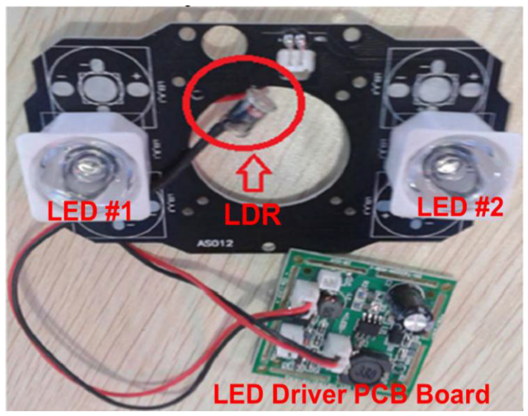
Figure 1 shows a demonstration board design which is implemented with the light-dependent resistor (LDR), the light-emitting diode (LED), and an LED driver printed circuit board (PCB). The typical LED driver with the LDR operates with a large dark current.
In this study, a CA with enhanced dark current cancellation was fabricated using 0.18 µm 1P2M CMOS technology with a chip area of 762 μm × 452 μm, including pads. Simulated and measured results were obtained with white LED light and characterized using a lux meter at a supply voltage
VCC of 3.3 V, an external resistance
RSS of 10 kΩ, and an environmental temperature varying from −40 °C to 125 °C. The rest of this paper is organized as follows.
Section 2 elucidates the proposed circuit topology of the light detector.
Section 3 presents the simulated and measured results, and in
Section 4, conclusions are drawn.
2. Proposed Circuit Topology of the Light Detector
In this section, we propose a CA with dark current cancellation that is composed of a dark diode (DD) and a photodiode (PD). The DD senses the dark current in dark environment, while the PD senses the photodiode current in electric lighting.
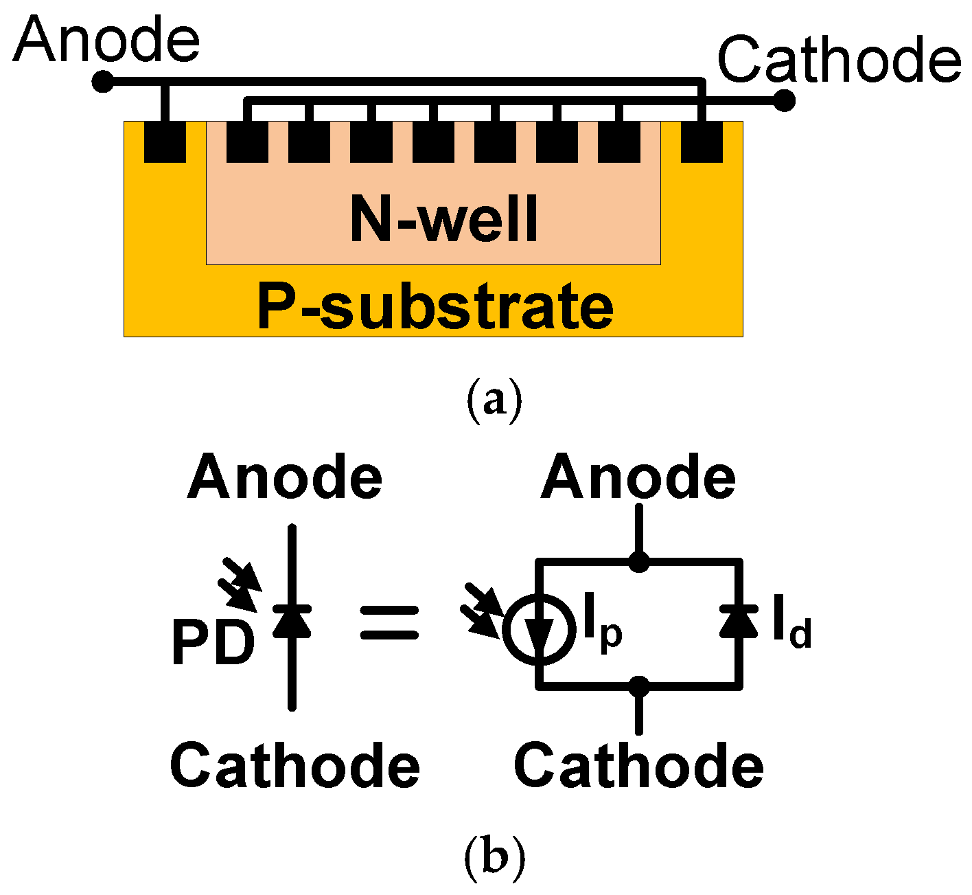
Figure 2 presents the schematic cross-section of an n+/p-substrate PD and its equivalent circuit. The PD is built with a p-n junction, which is sensitive to the environmental temperature.
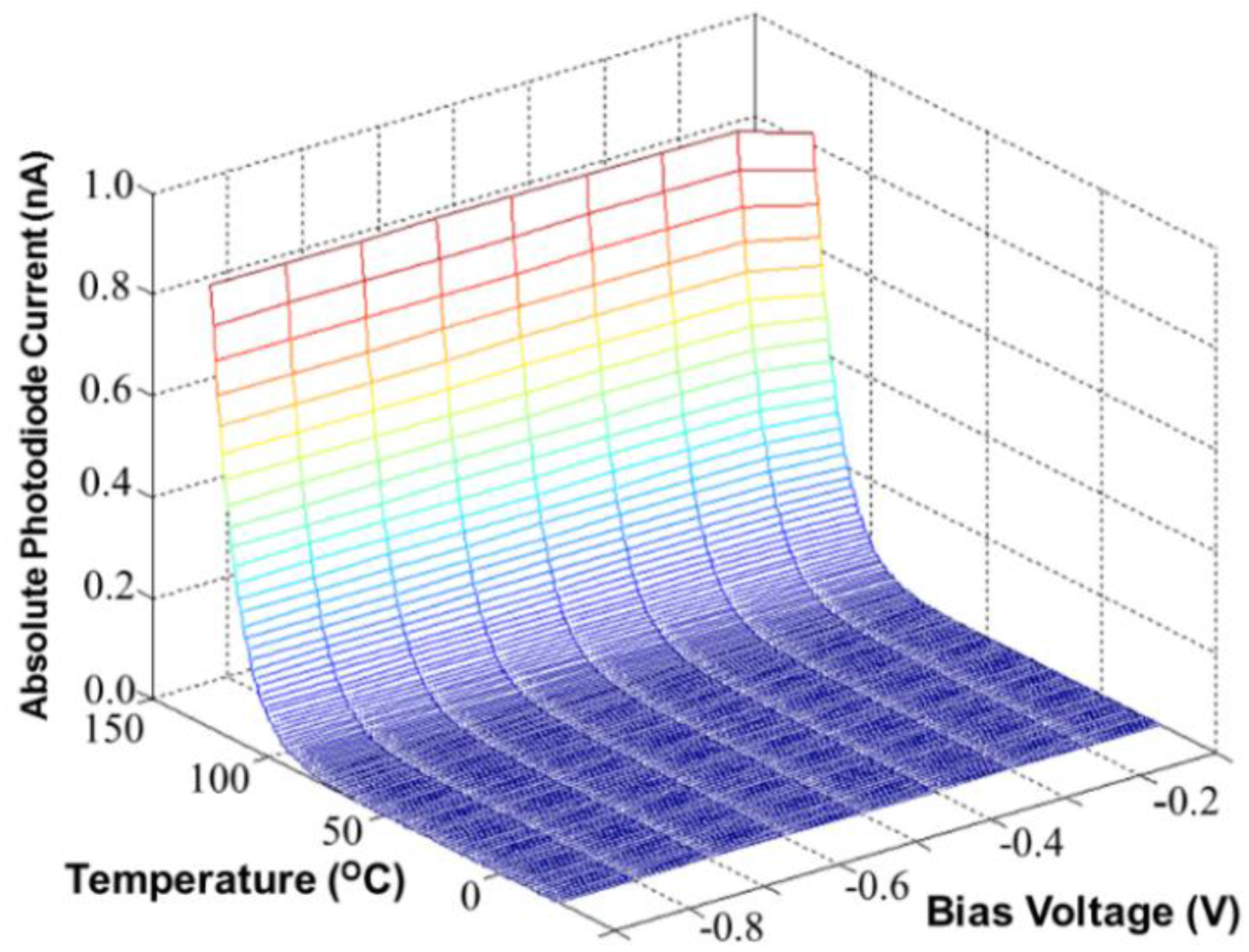
Figure 3 shows the simulated PD dark current as a function of environmental temperature (°C) and bias voltage (V) in dark conditions. According to the simulated results, the PD dark current (nA) is highly sensitive to the environmental temperature, but insensitive to the bias voltage.
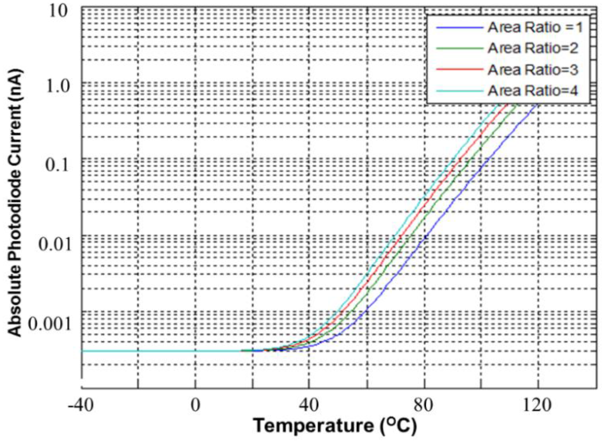
Furthermore, the sensing area of the PD is another important factor. The simulated dark current is approximately proportional to the area ratio, which is defined as the ratio of the PD area to 300 μm × 300 μm.
Figure 4 shows the simulated dark current as a function of the environmental temperature (°C) in dark conditions. The smaller the area ratio is, the smaller the dark current is. All simulated dark current levels are settled to 0.3 pA due to imperfect diode model, which is provided from foundry.
Figure 5 shows the CA of the PD, which operates without dark current cancellation. The resistance of the PD
RPD is equal to the voltage drop
VPD in the PD divided by its current
ILight. The light current of the PD
ILight is amplified with a current mirror, whose magnification is approximately equal to (
W2/
W1) × (
W4/
W3) × (
W6/
W5) with equal length (
L) for all MOSFETs. Thus, the output current
IO can be expressed with the total current gain A:
where
ILight, also called the photodiode current, includes the illumination current
ILux and the dark current
IDark, which flow from
VDD to the ground in a dark environment. The photocurrent
ILight and dark current
IDark are amplified A times. If the CA operates in a variable-temperature system without dark current cancellation, the dark current causes malfunction. This is the reverse of the characteristic of p-i-n PDs. For a reverse biased diode, the reverse bias current I
R can be defined by the following equation with reverse bias voltage
V [
8]:
where
IS is the saturation current,
q is the electronic charge,
kT is the Boltzman energy, and
n is a parameter of which the value depends on contributions from both diffusion and surface-generation currents. For a 4H-SiC avalanche photodiode (APD), the dark current is close to the measurement limit at low bias levels. At high bias, the dark current is relatively insensitive to temperature, a characteristic that signifies tunneling. If we assume that the tunneling dark current undergoes avalanche multiplication similar to that of the photocurrent at high bias, the total dark current is expressed by reference [
9]:
where
Gain(
V,
T) is an additional correction factor obtained through photocurrent measurement. The tunneling current
Itunneling is proportional to
A ×
V3/2 with the device area
A and the effective bias voltage
V [
9]. The objective of this study was to obtain a zero dark current in order to achieve higher photo resistance sensitivity.
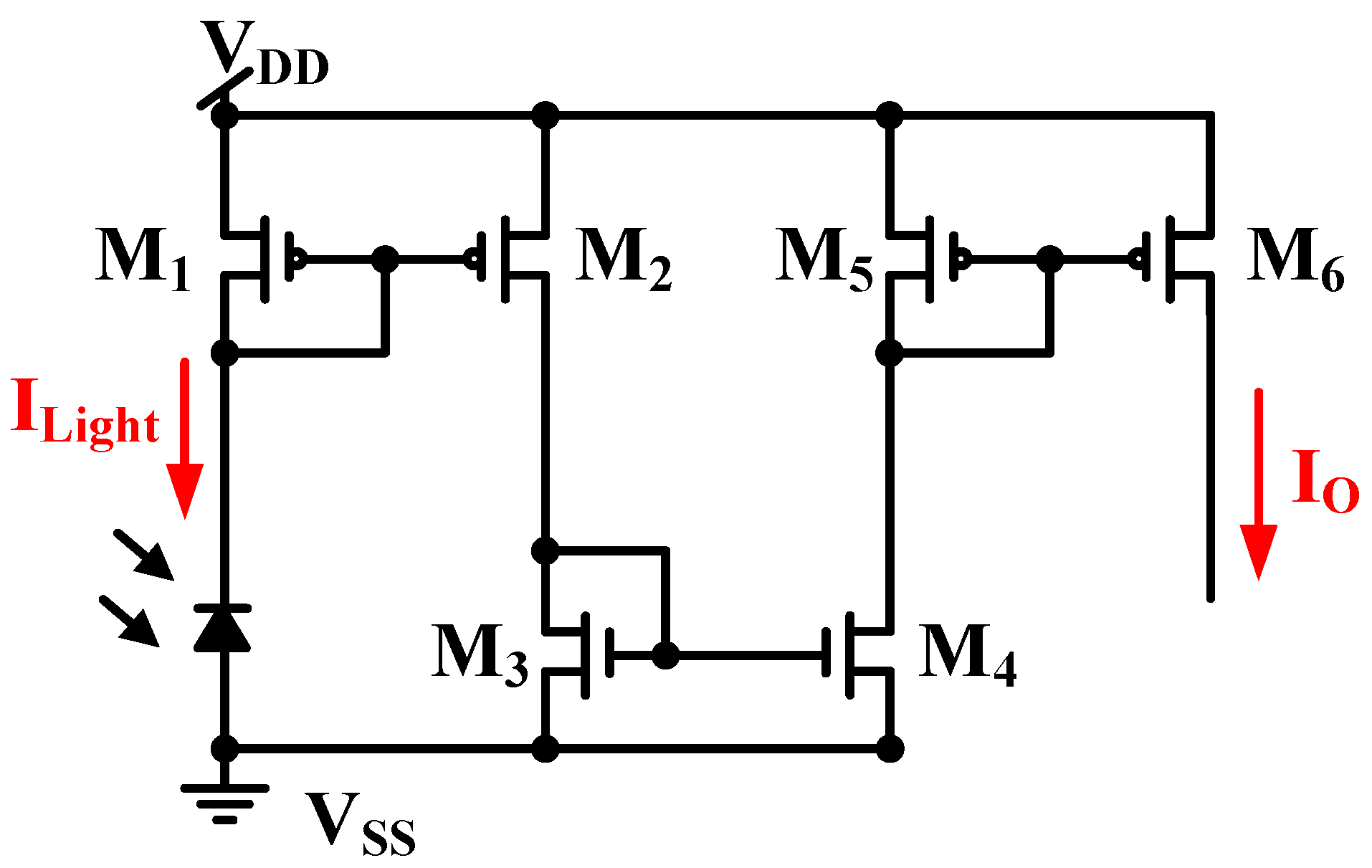
Figure 6 shows a CA with dark current cancellation that is composed of a dark diode (DD) and a PD [
10]. The DD senses the dark current
IDark in dark environments, while the PD senses the photodiode current
ILight in electric lighting. The photodiode size of PD (
APD) is two times of that of DD (A
DD); and the MOSFET size of
M2 is two times that of
M1, e.g.,
APD = 2 ×
ADD and (
W/
L)
M2 = 2 × (
W/
L)
M1. Thus, the drain current
ID3 of
M3 is equal to the illumination current
ILux and the output current I
O is expressed by:
where (
W/
L)
n is the metric ratio of transistor
Mn, and
B is the current gain. That is, (
W/
L)
M3 = (
W/
L)
M4 and (
W/
L)
M6 =
B × (
W/
L)
M5. The output current I
O operates without the dark current I
Dark. That is, the dark current is cancelled in
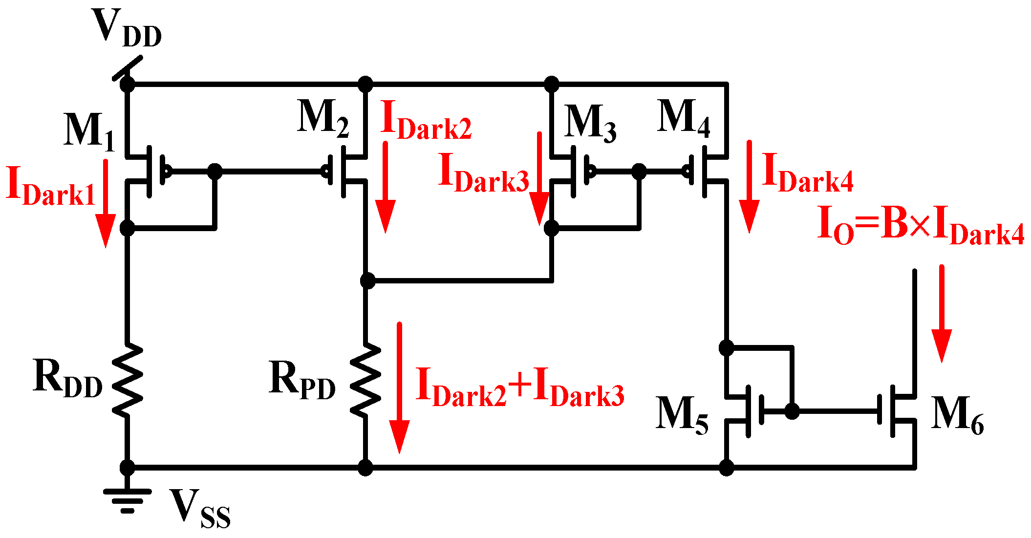
Figure 6. However, it is difficult to achieve a zero illumination current in light application because of the MOSFET mismatch in the CA. When both the DD and PD operate only with dark current, the two equivalent resistors of the DD and PD are expressed as R
DD and R
PD, respectively, and the current symbols,
IDark1,
IDark2,
IDark3, and
IDark4, denote the dark currents of
M1,
M2,
M3, and
M4, respectively, in dark conditions. As shown in
Figure 7, the output current I
O is achieved:
where
B is the current gain displayed in Equation (6) and is approximately 10,000 times. The output current
IO includes the amplified dark current of
M4. This circuit operates with a large dark current.
The dark current in
Figure 7 must be reduced.
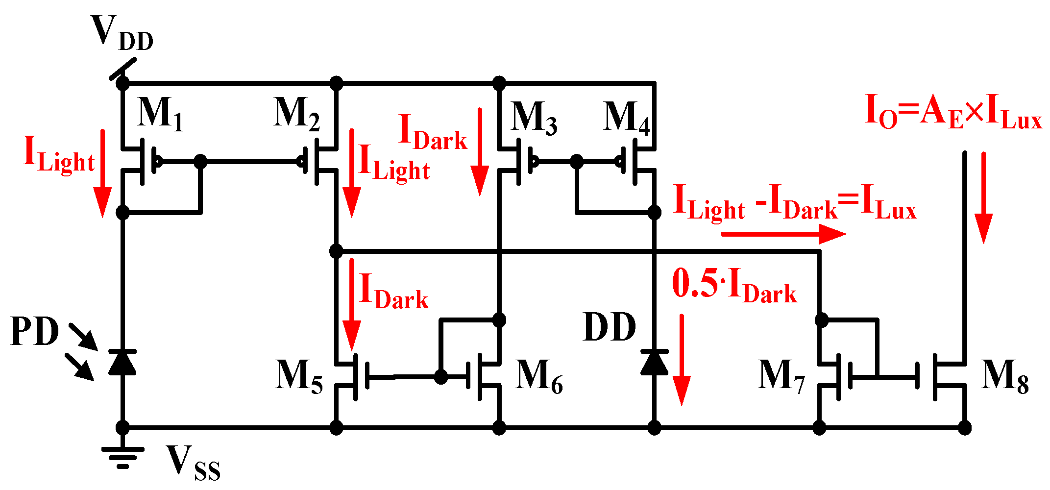
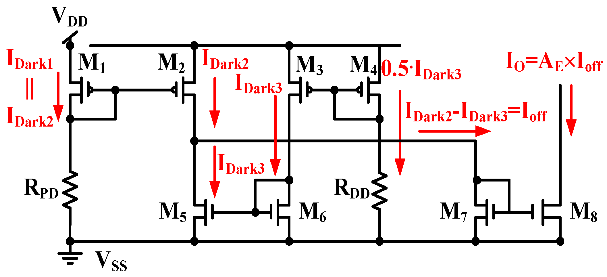
Figure 8 displays a CA with enhanced dark current cancellation. The MOSFET size of
M3 is two times of that of
M4, e.g., (
W/
L)
M3 = 2 × (
W/
L)
M4. As shown in
Figure 8, current steering is implemented to draw a different current,
ILight −
IDark, which is equal to the illumination current
ILux. The output current I
O can then be expressed with the total current gain
AE, if (
W/
L)
M1 = (
W/
L)
M2, (
W/
L)
M5 = (
W/
L)
M6, and (
W/
L)
M8 =
AE × (
W/
L)
M7. The output current I
O in
Figure 8 operates without the dark current.
When both the DD and PD operate only with dark currents, the two equivalent resistors of the DD and PD are expressed as R
DD and R
PD, and the current symbols,
IDark1,
IDark2, and
IDark3, denote the dark currents of
M1,
M2, and
M3, respectively. As shown in
Figure 9, the output current I
O is obtained.
where
AE is the current gain, as in Equation (7). The output current I
O can be reduced to approximately zero if the dark current of
M2 is approximately equal to that of
M3 (
IDark2 ≈
IDark3). The proposed circuit can also suppress the dark current induced by the environmental temperature, as described in Equation (3).
3. Simulated and Measured Results
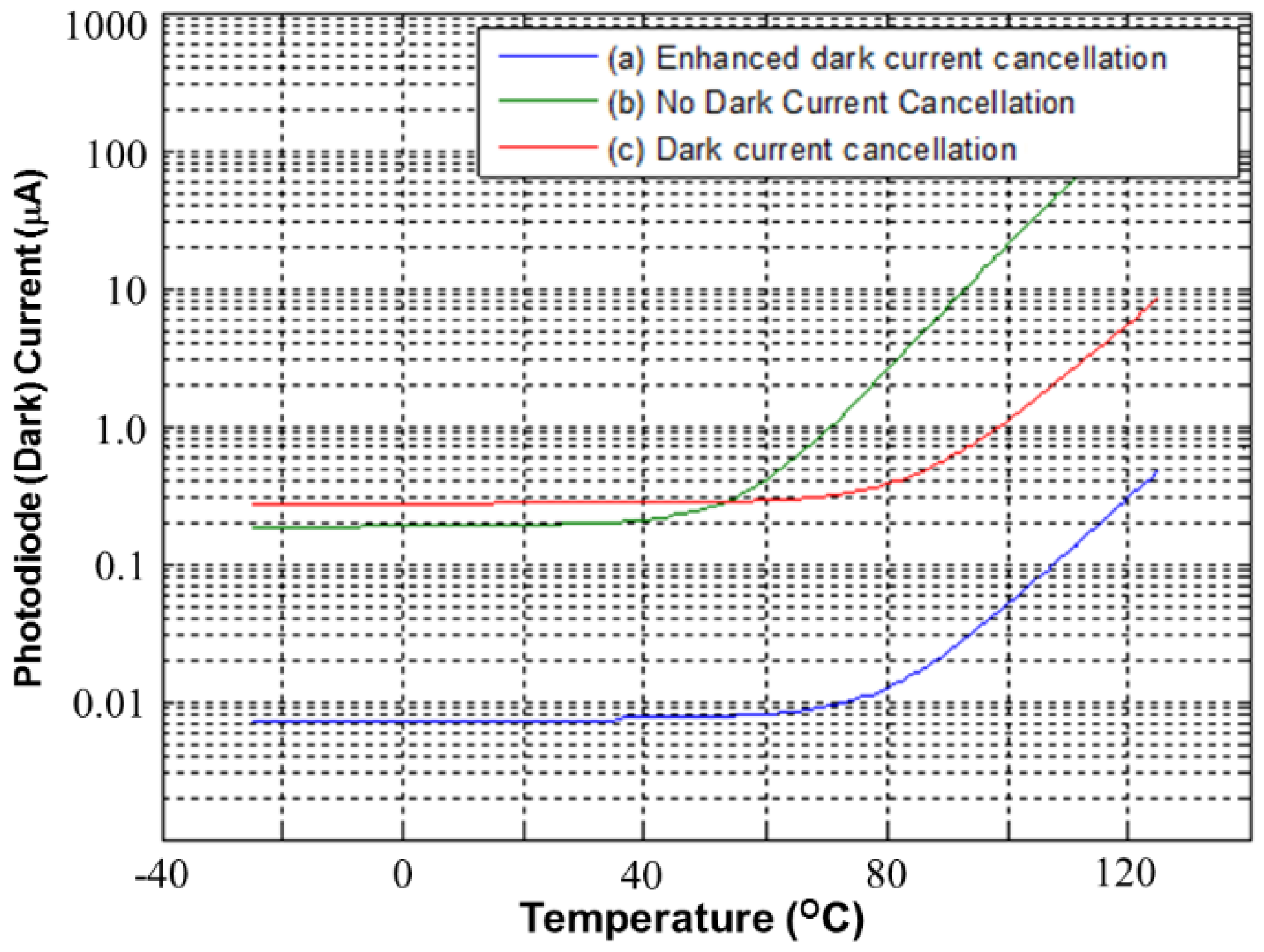
Figure 10 presents the simulated PD dark current versus temperature for CAs. Three types of CA were compared. First, the proposed CA with enhanced dark current cancellation is indicated by
Figure 10a. Next, a CA without dark current cancellation is denoted by
Figure 10b. Finally, a CA with dark current cancellation is denoted by
Figure 10c. According to the simulated results, the proposed CA with enhanced dark current cancellation operates with the lowest dark current. This means that the dark current can be cancelled perfectly with the proposed CA. The CA without dark current cancellation, which is denoted by
Figure 10b, operates with a larger dark current. Note that the dark current level of curve
Figure 10c is higher than that of
Figure 10b below approximately 50 °C, because the magnification of curve
Figure 10c is higher than that of curve
Figure 10b.
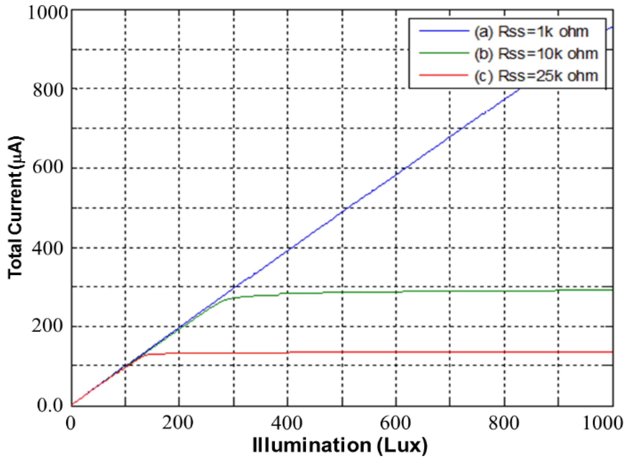
Figure 11 shows the simulated total current I
DD of the proposed CA as a function of illumination at three external resistances, namely
RSS = 1 kΩ,
RSS = 10 kΩ, and
RSS = 25 kΩ. As shown in
Figure 11, a lower
RSS expands the illumination detection range. Two higher resistances,
RSS = 10 kΩ and
RSS = 25 kΩ, sharply force the proposed CA into saturation at 280 lux and 140 lux, respectively. Thus, for wide application, selecting a low
RSS is beneficial.
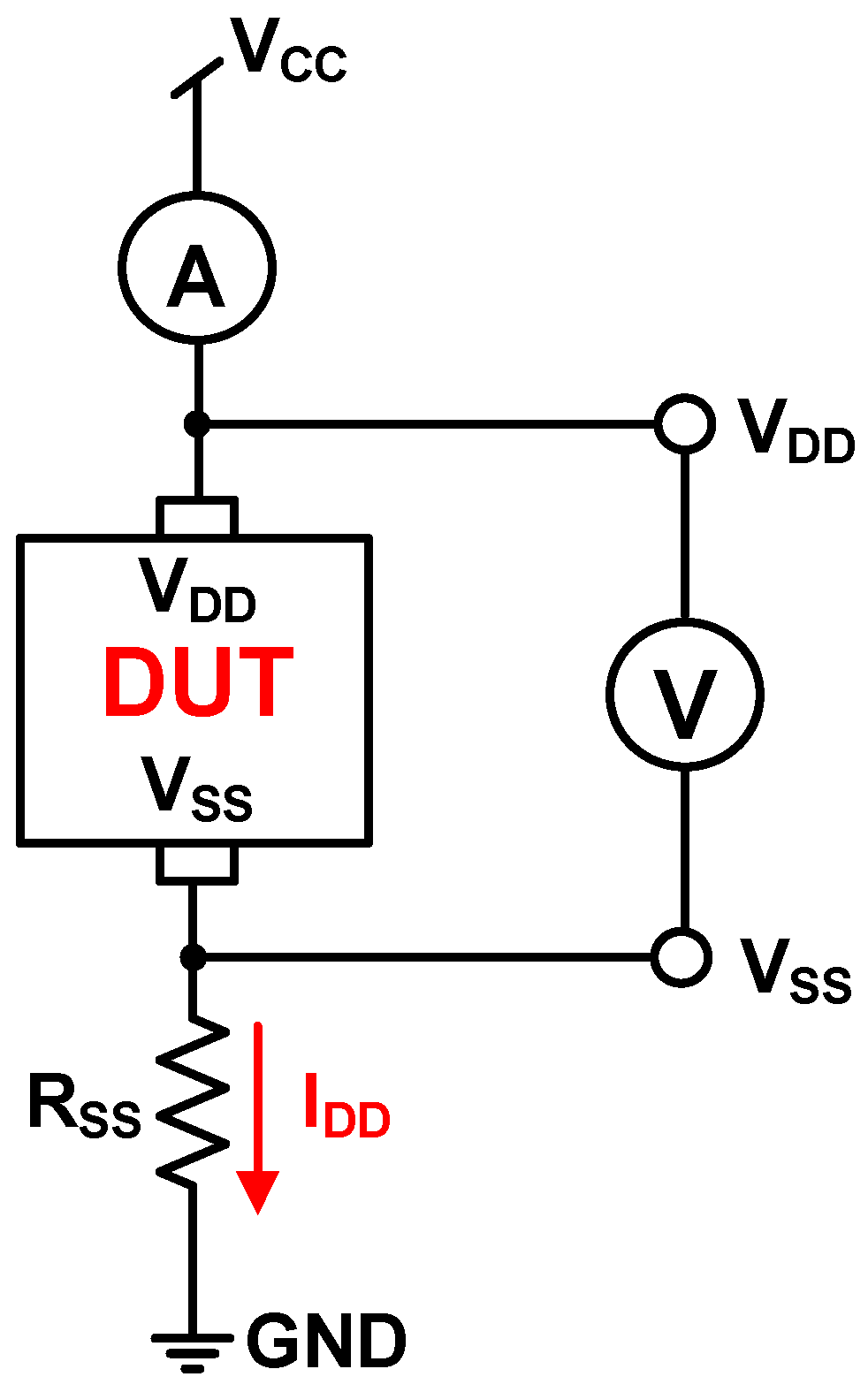
Figure 12 shows the setup of the proposed CA that was used for measurement, with a current meter (A), voltage meter (V), and the design under test (DUT) chip. The external resistance
RSS was used to measure the total current I
DD, which was varied by applying illumination (lux) with white LED light.
Table 1 and
Table 2 summarize the simulated and measured dark current
IDark and total current I
DD of the proposed CA with enhanced dark current cancellation at the PD area of 300 μm × 300 μm and a PD to DD area ratio of 2 times.
Table 1 indicates that the measured dark currents are smaller than those of the simulations. This is because the PD model was always adopted in the simulations, but is not proven in the silicon process. However, the measured total currents are larger than those of the simulations. The total light current is approximately linear as a function of illumination in the simulation and the measurements in
Table 2.
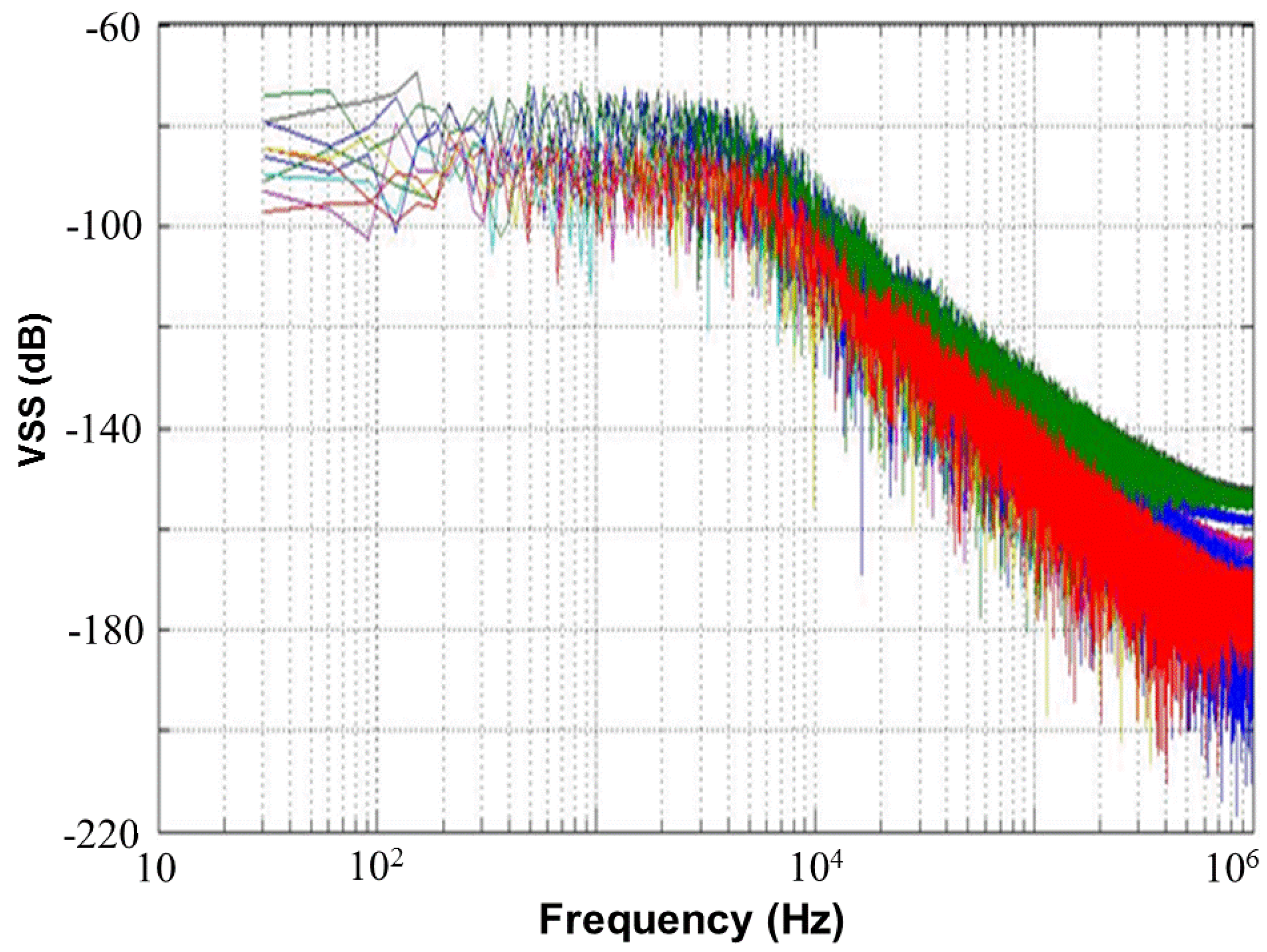
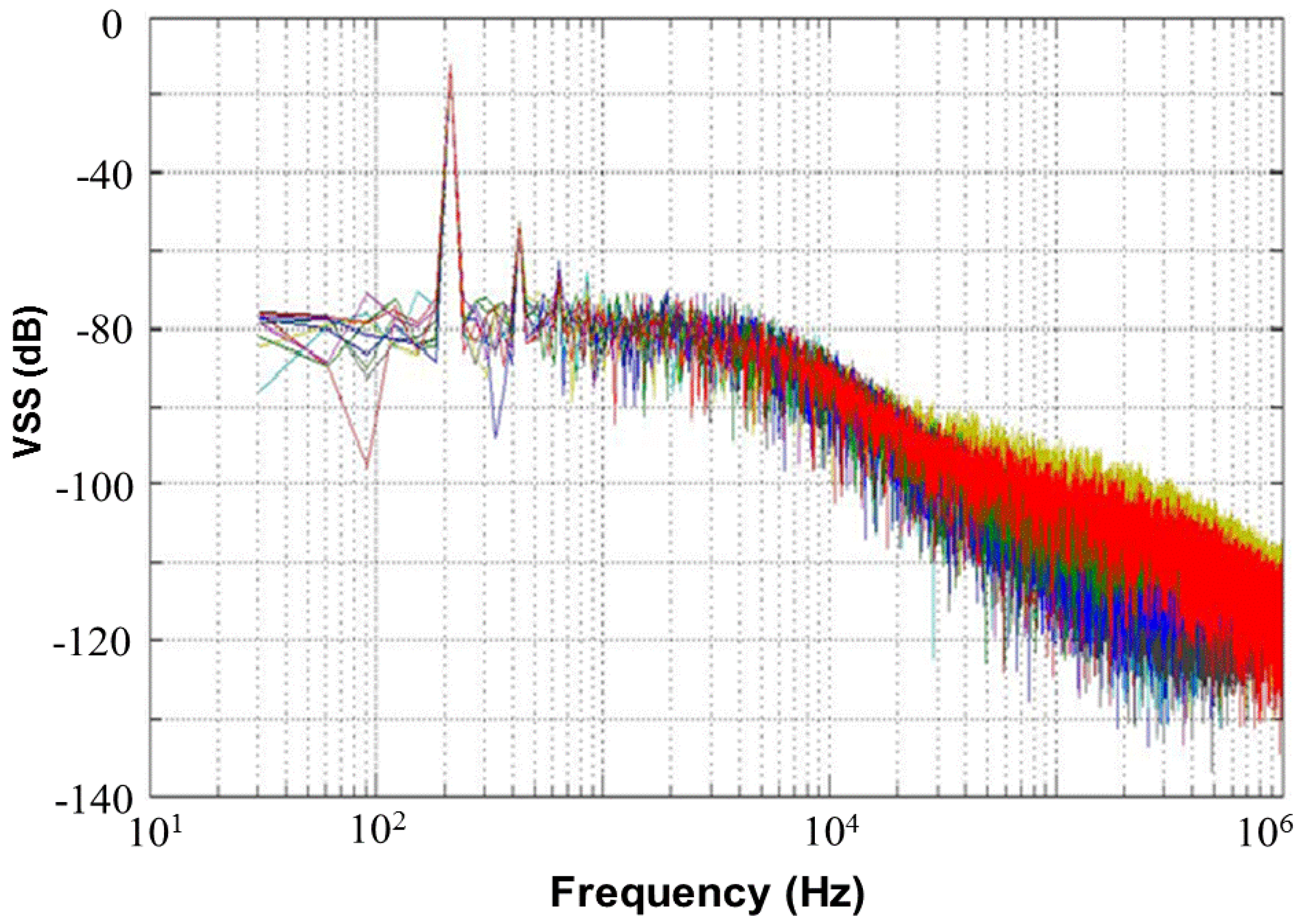
Figure 13 shows a 65,536-point FFT simulation with a noise level of 80 dB and an external resistor
RSS of 1 kΩ for the proposed CMOS light detector. This figure presents a simulated frequency response of 10 Monte Carlo samples with random noises at node
VSS, which is shown in
Figure 12. If a photodiode current signal, which is a superposition of a 250 lux (peak-to-peak) noiseless sine wave with a frequency of 210 Hz and a DC 500 lux, is fed to the proposed CMOS light detector, a plot of the frequency response of the simulated 10 Monte Carlo samples with random noises is made in
Figure 14 at node
VSS for the proposed light detector. The current signal with frequency of 210 Hz performs without any random noises.
Table 3 shows the simulated total harmonic distortions (THDs), signal-to-noise ratios (SNRs), and signal-to-noise+distortion ratios (SNDRs) of the 10 Monte Carlo samples with random noises at node
VSS of
Figure 14 for the proposed light detector. As shown in
Table 3, those simulated results of THD, SNR, and SNDR are roughly consistent. The Monte-Carlo approach can capture very nonlinear noise behaviors.
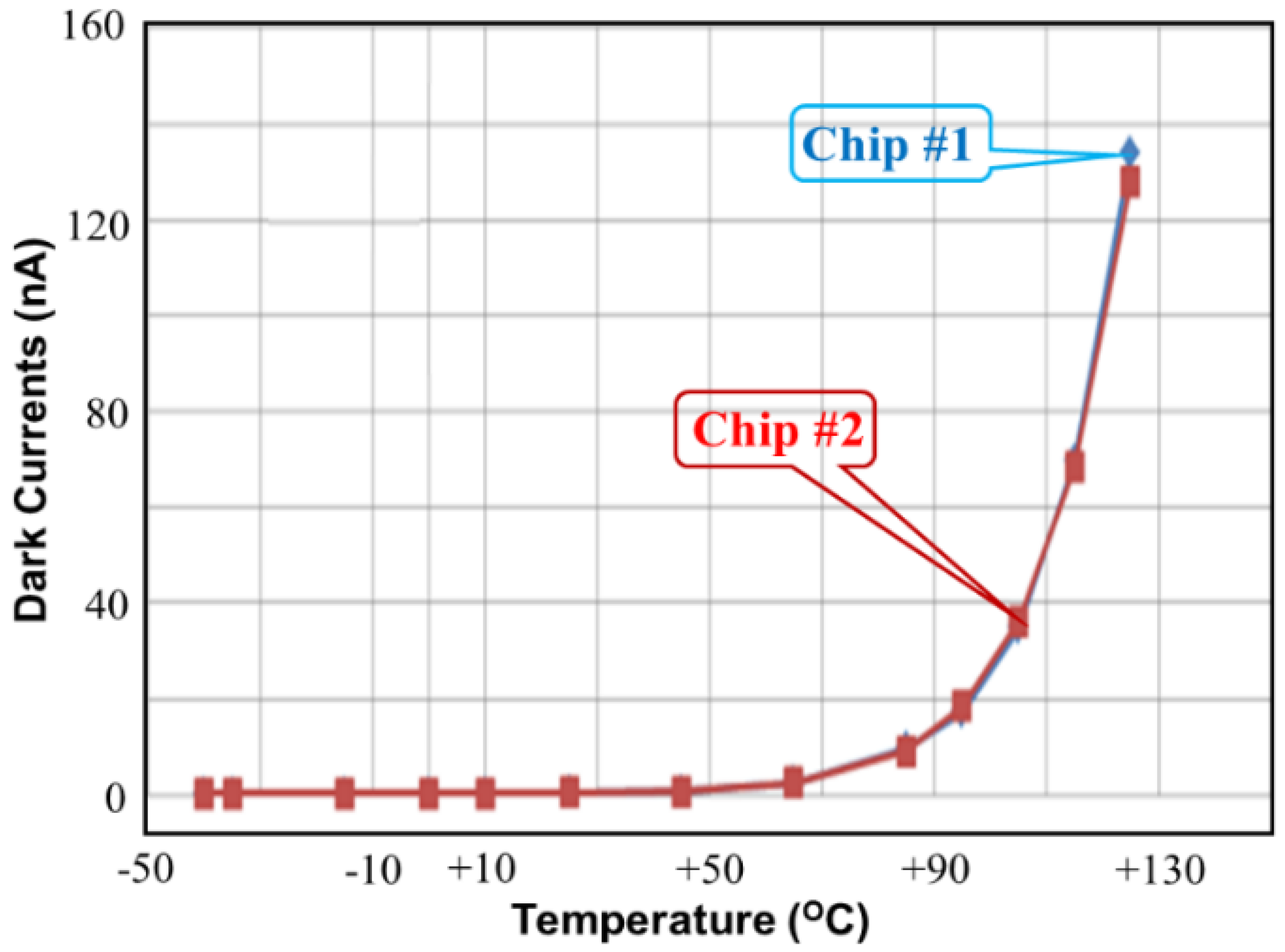
Figure 15 shows the measured dark current versus temperature for the proposed CA with enhanced dark current cancellation. The maximum dark current is approximately 135 nA at 125 °C. This measurement proves that the proposed CA performs with low dark current as a function of the environmental temperature. According to the measurements in
Figure 15, the device performs with zero dark current at temperatures lower than 50 °C and exhibits an exponential relation at temperatures higher than 50 °C. Notice that two measured dark currents are consistent in
Figure 15, although chip #1 and chip #2 perform with different maximum dark currents at 125 °C.
Table 4 summarizes the measured dark currents versus temperature of the proposed CAs, Chap #1 and Chip #2.
Table 5 summarizes the measured output currents with respect to the illumination of the proposed CAs. According to the measured output currents in
Table 5, the proposed CA performs with good linearity and wide illumination range.
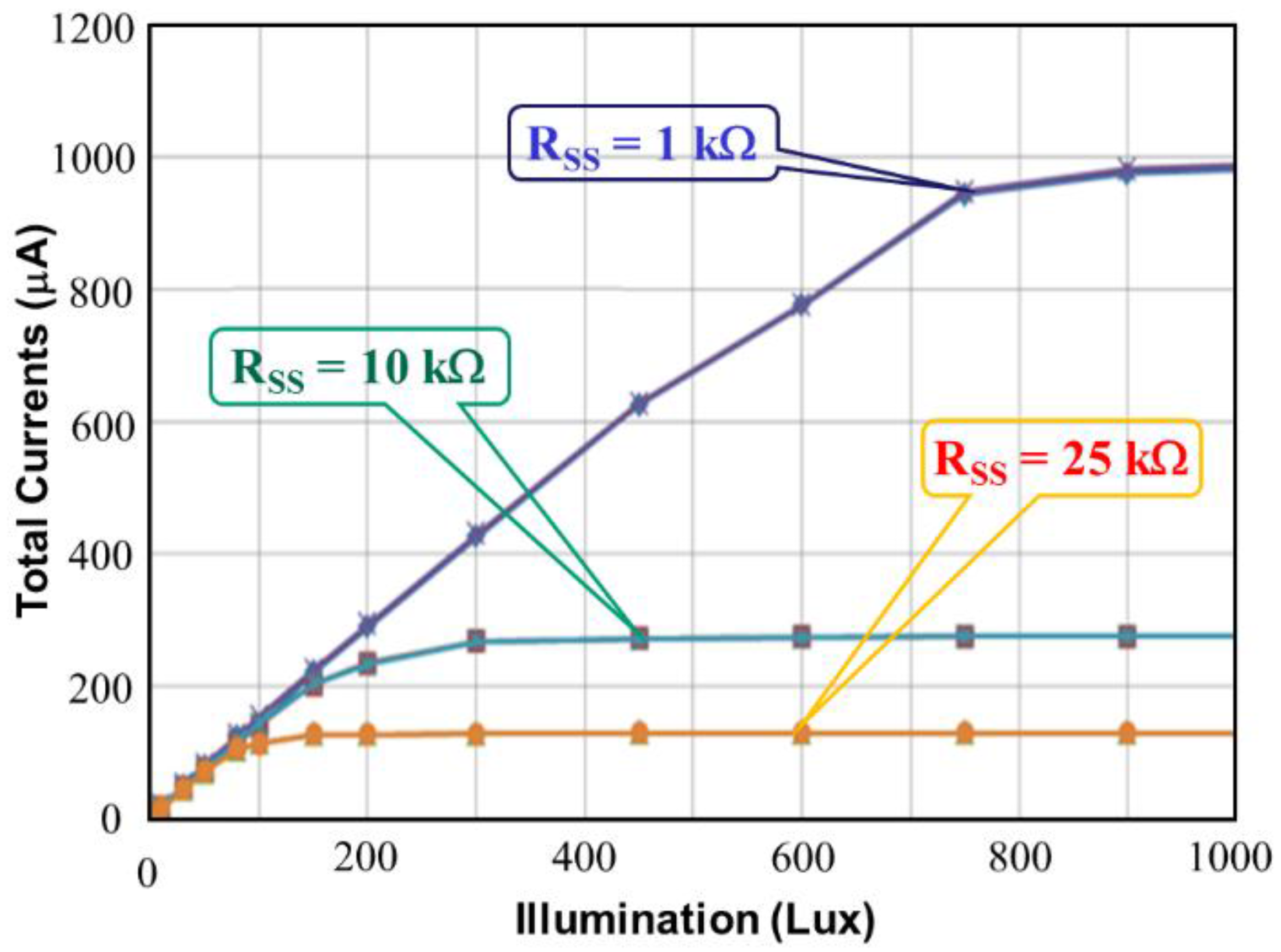
Figure 16 shows the total current as a function of illumination (lux) for the proposed CMOS light detector with dark current suppression at room temperature. The larger
RSS is, the lower the total current. As shown in
Figure 16, two curves with
RSS = 10 kΩ and
RSS = 25 kΩ indicate saturation at low illumination, but the curve with
RSS = 1 kΩ does not display saturation until 1000 lux. The measured total currents
IDD match those in
Figure 11.
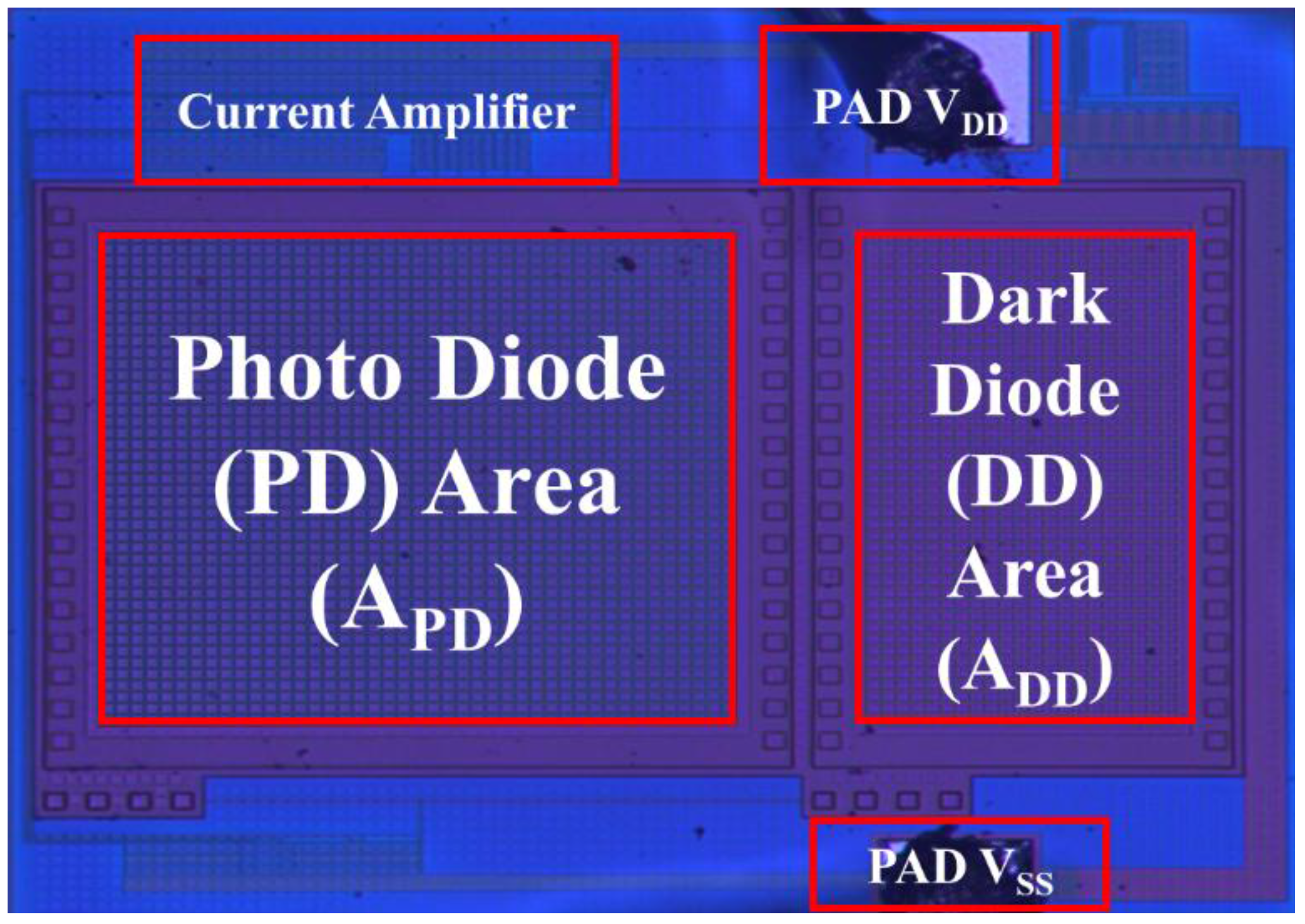
Figure 17 shows the microphotograph of the proposed CMOS light detector with dark current suppression in a variable-temperature system. Note that the PD area
APD is twice as large as the DD area
ADD. This arrangement not only lowers the dark current by contracting A
DD but also enhances the luminous efficiency by enlarging
APD.


