1. Introduction
The Hall plate is a major magnetic sensor, which is fabricated using CMOS technology, for sensing the magnetic induction perpendicular to the Hall plate surface and converting it into a corresponding electrical signals such as voltage, current, and frequency [
1,
2,
3]. To enhance the linear characteristics of a current-mode Hall sensor, various compensated techniques have been developed [
4,
5,
6]. The Hall plate performs with low-voltage-related magnetosensitivity compared with a magnetotransistor or magnetic MOSFET (MAGFET) [
7]. A split-drain MAGFET is widely used as a Hall sensor for sensing the magnetic induction perpendicular to the MAGFET plane, in which a current difference is obtained between two adjacent drains of the MAGFET [
8]. The relative sensitivity depends on the primary geometric parameters and biasing conditions of the applied magnetic device [
9,
10]. A symmetrical and differential structure performs with effective sensitivity [
8]. In addition, the strip approach is considered to transmit a biasing current of up to 500 mA, whereas in the coil approach, the biasing current is limited to 20 mA [
11]. The strip MAGFET with two sources is superior to that with a shared source in terms of the biasing current. In the present study, CSHP was used to detect the applied magnetic induction and to induce the differential Hall voltages, which was connected to two gates of two separated MOSFETs and generated two separated drain currents. An output voltage was obtained using a readout circuit. Notably, the magnetosensitivity was enhanced because the drain current of the MOSFET was a quadratic equation of the induced Hall voltage, which was equal to the gate voltage of the MOSFET, and the offset voltage will be effectively eliminated by the differential topology of the CSHP [
12].
Magnets and magnetic induction sensing devices are often attractive in instrumentation because they can be operated in noncontacting conditions and are small in size [
13]. However, the magnetic induction decays with distance according to the power–law relationship. A magnetic induction sensing device with a high sensitivity to small magnetic induction and linear response to human motion should be selected [
13]. Notably, the magnetic induction strength is in the order of tens of Gauss. The proposed device in [
13] could be useful in situations that require noncontacting displacement measurements. In addition, a linear bidirectional moving-magnet actuator with elastic magnetic force was presented in [
14], which is an arrangement of two linear radiometric Hall sensors and a small permanent magnet disc attached to the mobile actuator’s rod that moves between the two fixed sensors. An open-loop method, proposed by Arcire [
14], uses an analog flux density transducer based on the Hall effect with a microcontroller board for acquiring and processing the analog data delivered by the transducer. The determination of the displacement around a neutral equilibrium position is easy. Moreover, Netzer described two linear methods for noncontacting position measurement based on a relative movement between a Hall-element magnetic sensor and contact gradient static magnetic induction [
15]. The induction intensity at the edges of the linear range was approximately ±300 G, and the maximum error due to the earth’s magnetic induction of ±0.3 G was approximately 0.1%. In addition, a new position detecting system by using the magnetic flux of the magnet on the mover was proposed, in which a Hall element was considered in a flux sensor for a synchronous motor [
16]. Moreover, an intelligent odometer was studied using the Hall effect to avoid the mechanical odometer defect. The speed and mileage were measured using the Hall sensor through the pulse detection method [
17].
For distance detection, an unconventional method was proposed to identify the lane markings on a road surface through laser measurement system. This method was achieved using the reflection of the laser beam [
18]. Fall detection in elderly residents was performed using an infrared distance sensor [
19]. Furthermore, the Poisson distance image was acquired by solving the two-dimensional Poisson equations defined on the spatial–temporal accumulative image, and the action descriptors were fed into the nearest neighbor classifier to recognize daily actions, particularly to detect the abnormal fall action [
20]. In addition, an advanced driver assistance was presented to complete the measurement of the distance between a vehicle and the detected object. Particular attention has been given to the vision-based technique because it is considered one of the most accurate systems for identifying targets and measuring the distance from the target to the vehicle [
21]. In brief, distance measurement can be completed using techniques such as laser beam, infrared sensor, visual-based fall detection, and vision-based technique. However, both laser beam and infrared sensor are oriental sensors, and the visual-based fall detection and vision-based technique operate in a bright environment. The object to be measured cannot be detected if it is located in the dark or has diverged from the oriental range even when it is considerably closer to the sensor. To resolve these faults, the current study proposes a distance detecting method by using the strip MAGFET, which includes two separated MOSFETs, a differential polysilicon CSHP, and a readout circuit.
The proposed distance detector could detect the distance from the magnetic body (human) to the magnetic sensor by sensing the magnetic induction of the magnetic body perpendicular to the chip surface. The strip MAGFET not only increased the magnetosensitivity but also eliminated the offset voltage which is generated because of the device mismatch and Lorentz force [
22]. Moreover, a commercial instrumentation amplifier (IA) INA333 was applied to amplify the output voltage of the readout circuit and increase the detecting distance. The remainder of this paper is organized as follows.
Section 2 describes the operational principles of the proposed distance detector.
Section 3 presents the readout circuit for the distance detector.
Section 4 presents some simulated and measured results.
Section 5 presents discussion followed by conclusions.
2. Operational Principles of the Distance Detector
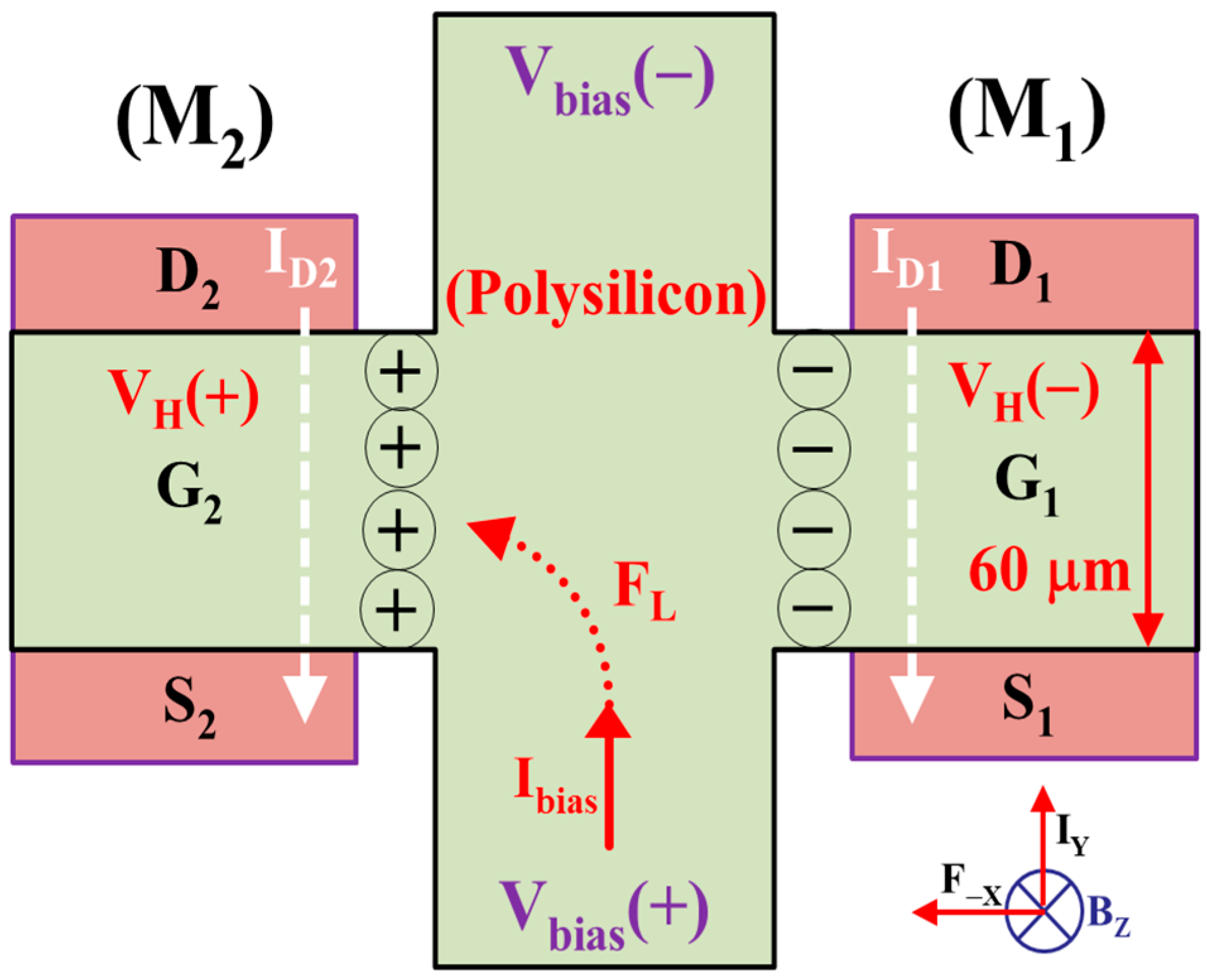
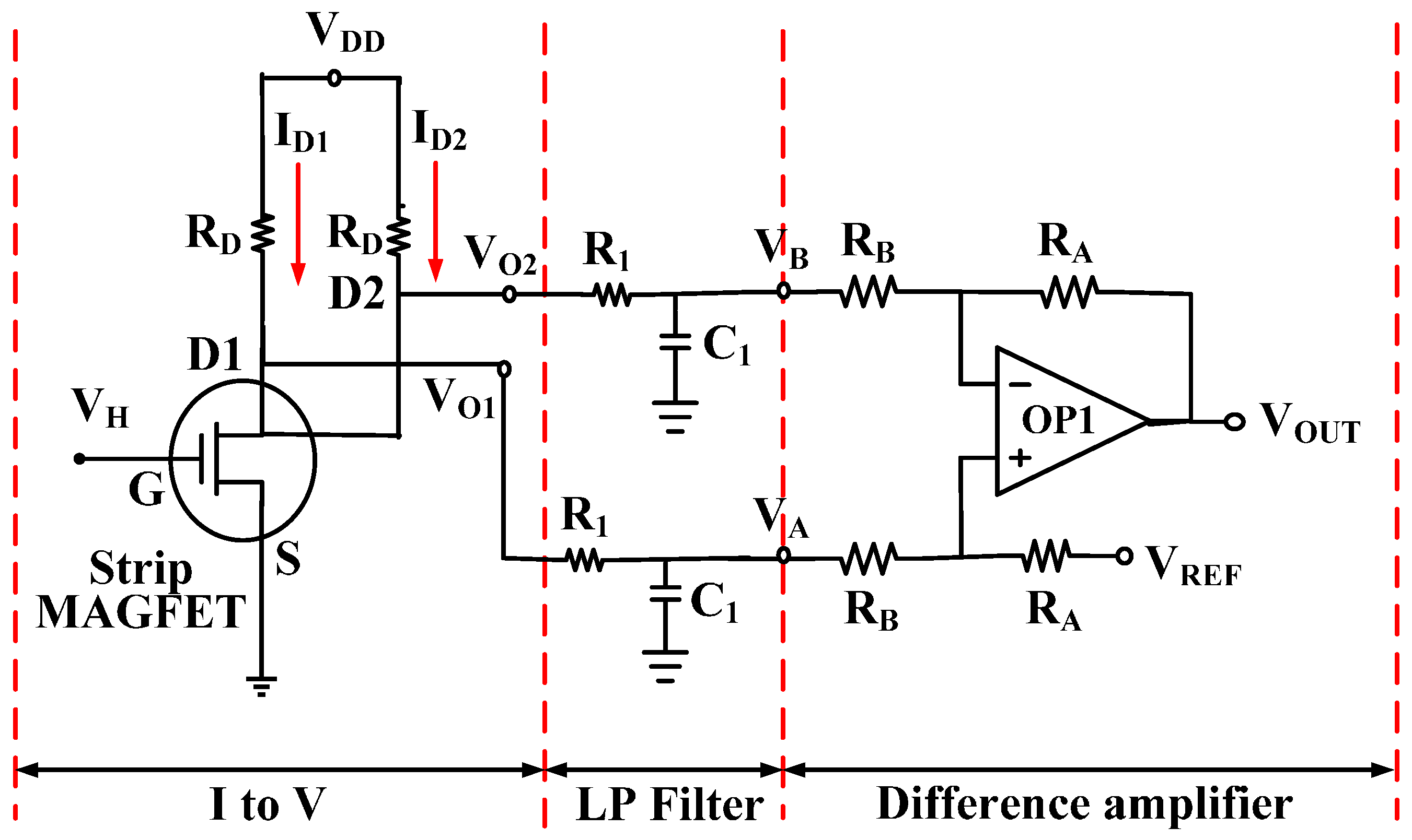
Figure 1 presents a strip MAGFET, which is composed of two separated MOSFETs, M1 and M2, and a differential polysilicon CSHP, for sensing the magnetic induction
BZ perpendicular to the chip surface. The distance from the magnetic body (human) to the magnetic device (strip MAGFET) can be easily detected using the proposed magnetic sensor.
Ibias is the biasing current in the
y-direction and
F−X is the Lorentz force in the
x-direction, reversely. The differential topology not only effectively cancels the offset but also doubly enhances the magnetosensitivity. A polysilicon CSHP is located on two identical MOSFETs to establish a strip MAGFET with high biasing current [
8]. In the absence of the applied magnetic induction
BZ, two drain currents,
ID1 and
ID2, are the same at D
1 and D
2 of the MOSFETs, M
1 and M
2, respectively. After passing through the readout circuit, which includes a current-to-voltage (I-to-V) converter, a low-pass filter (LPF), and a difference amplifier (DA), the output voltage
VOUT of the DA is constant. That is, ∆
VOUT = 0. By contrast, the output voltage
VOUT is a function of the bias current versus applied magnetic induction.
In general, the voltage-mode Hall devices can be biased in two modes: voltage biasing and current biasing. In the current biasing mode, the current-related sensitivity
SRI is calculated as follows [
23]:
where the unit of
SRI(B) is V·A
−1·T
−1,
Ibias represents the supply bias current,
∆B represents the change in the applied magnetic induction, and ∆
VOUT represents a variation in the DA output voltage [
23]. However, the proposed strip MAGFET detects the distance
∆D between the magnetic sensor and magnetic body. Thus, the current-related sensitivity should be redefined as follows:
where the unit of
SRI(D) is V·A
−1·m
−1. In addition, the nonlinearity error (
NLE) is defined as
where the unit of
NLE is % and ∆
V(0)OUT represents the calculated output voltage difference based on the slope of the straight line obtained from the best fit to the output characteristic [
24]. The operational principle of the strip MAGFET is described below.
As shown in
Figure 1, two identical MOSFETs, M
1 and M
2, are operated in the saturation mode. If a magnetic induction
BZ and a bias current
Ibias are applied to the polysilicon CSHP, the positive and negative Hall voltages,
VH(+) and
VH(−), are generated by Lorentz force
FL in the
x-direction reversely and
x-direction, respectively. In other words, the gate voltage of M
2 is larger than that of M
1. By grounding two sources, S
1 and S
2, two drain currents,
ID1 and
ID2, can be expressed as follows:
and
where
μn,
Cox,
W,
L, and
VTH represent the mobility of electrons, parasitic capacitance per unit gate area, width, length, and threshold voltage, respectively.
VGS1 and
VGS2 represent the differential gate-to-source voltages of M1 and M2, respectively, with magnetic induction, whereas
VGS represents the gate-to-source voltage without magnetic induction. Subsequently, the induced Hall voltage
VH is derived from the Lorentz force.
where
represents the Hall coefficient,
Ibias represents the bias current in the
y-direction,
BZ represents the magnetic induction in the z-direction, and
t and
G represent the polysilicon thickness and geometrical correction factor, respectively [
24]. Thus, the current difference between
ID1 and
ID2 can be expressed as follows:
Rewriting Equation (8), we have
As shown in Equation (9), the current difference ∆ID is directly proportional to the bias current Ibias and the magnetic induction BZ. If the bias current Ibias is set as constant, the larger the magnetic induction BZ is, the higher the drain current difference ∆ID is. The physical mechanism may be that the Lorentz force FL pushes the positive charge to the left to gather at the left side of the polysilicon CSHP, which is connected to the gate terminal G2 of the second MOSFET (M2). Moreover, the electron current is directly injected into the right side of the polysilicon CSHP, which is connected to the gate node G1 of the first MOSFET (M1), to reduce the drain current of the first MOSFET (ID1). By applying a magnetic induction (~mT) to the magnetic sensor, an output voltage VOUT is acquired at the output node of the readout circuit by multiplying the drain current difference ∆ID with a resistor RD in the I-to-V converter and then multiplying approximately 16 times by RA = 100 kΩ and RB = 6.2 kΩ.
3. Readout Circuit
Two drain currents,
ID1 and
ID2, obtained at two separated drains of two MAGFETs over the considered magnetic induction range, are of the order of few milliamperes (mA). By passing through the I-to-V converter with resistor
RD and LPF with resistor
R1 and capacitor
C1, the high-frequency noise will be filtered out before the entering the DA.
Figure 2 presents the readout circuit of the proposed distance detector, which includes the I-to-V converter, LPF, and DA. Notably, the offset voltage can be effectively removed using the DA, and the single output
VOUT obtained is easy to use.
As shown in
Figure 2, an I-to-V converter was selected to convert the induced drain current, obtained from the proposed strip MAGFET, into a Hall voltage with drain resistor
RD. Two output voltages,
VO1 and
VO2, of the I-to-V converter can be expressed as follows:
where
VDD represents the power supply. The output voltage of the DA,
VOUT, passing through the LPF with resistor
R1 and capacitor
C1, is given by
where
VREF represents a constant reference voltage, which is used to adjust the output level.
∆ID (=
ID1 −
ID2) is defined as the drain current difference between the first and second drains of the MAGFET. For a DC magnetic induction,
s = 0, the small-signal output voltage
vout is given by
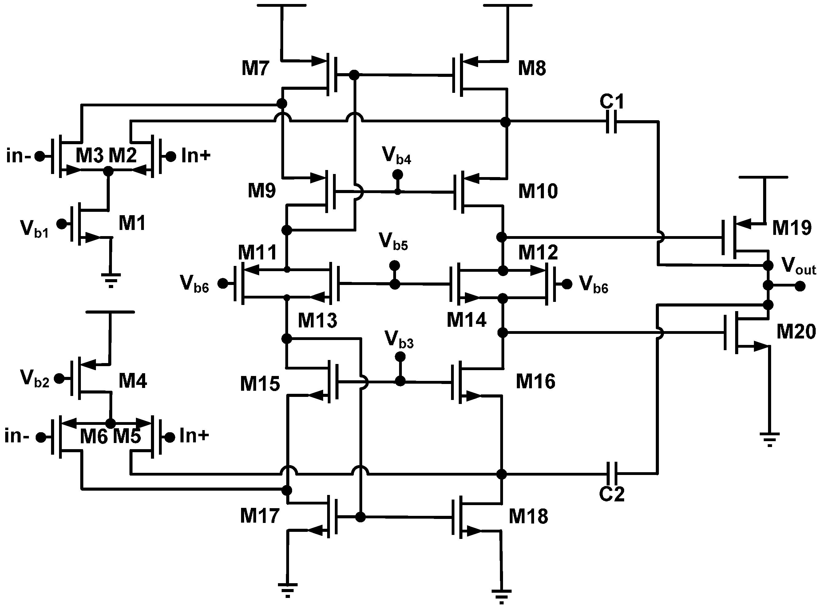
Figure 3 presents a low-voltage two-stage cascaded operational amplifier (opamp) with Miller compensation and compact class-AB output stage, which is composed of two common-source-connected output transistors, M
19 and M
20 [
25]. To make the quiescent current of the output transistors insensitive to supply voltage variations, the floating current source should have the same supply voltage dependency as the class-AB control. The value of the current source is set using two bias voltages, V
b5 and V
b6. The mirrors, M
7–M
10 and M
15–M
18, are loaded with the drain currents of the input pairs M
2–M
3 and M
5–M
6, respectively. These drain currents and the gate–source voltages of M7 and M17 change the common-mode input voltage. By adjusting two input bias currents with two bias voltages, V
b1 and V
b2, the common-mode input voltage approaches the positive supply rail or the negative supply rail. The opamp is compensated by using the conventional Miller technique including the cascode stages, M
12 and M
14, in the Miller loops. This compensation technique shifts the output pole to a frequency of approximately [
25].
where
gm0 represents the transconductance of the output transistors and
CL represents the load capacitor.
CM and
CGS,out represent the total Miller capacitor and the total gate–source capacitance of the output transistor, respectively.
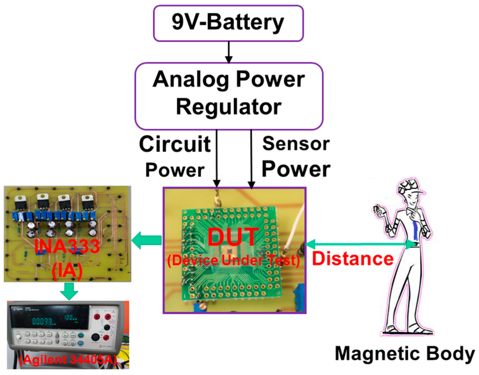
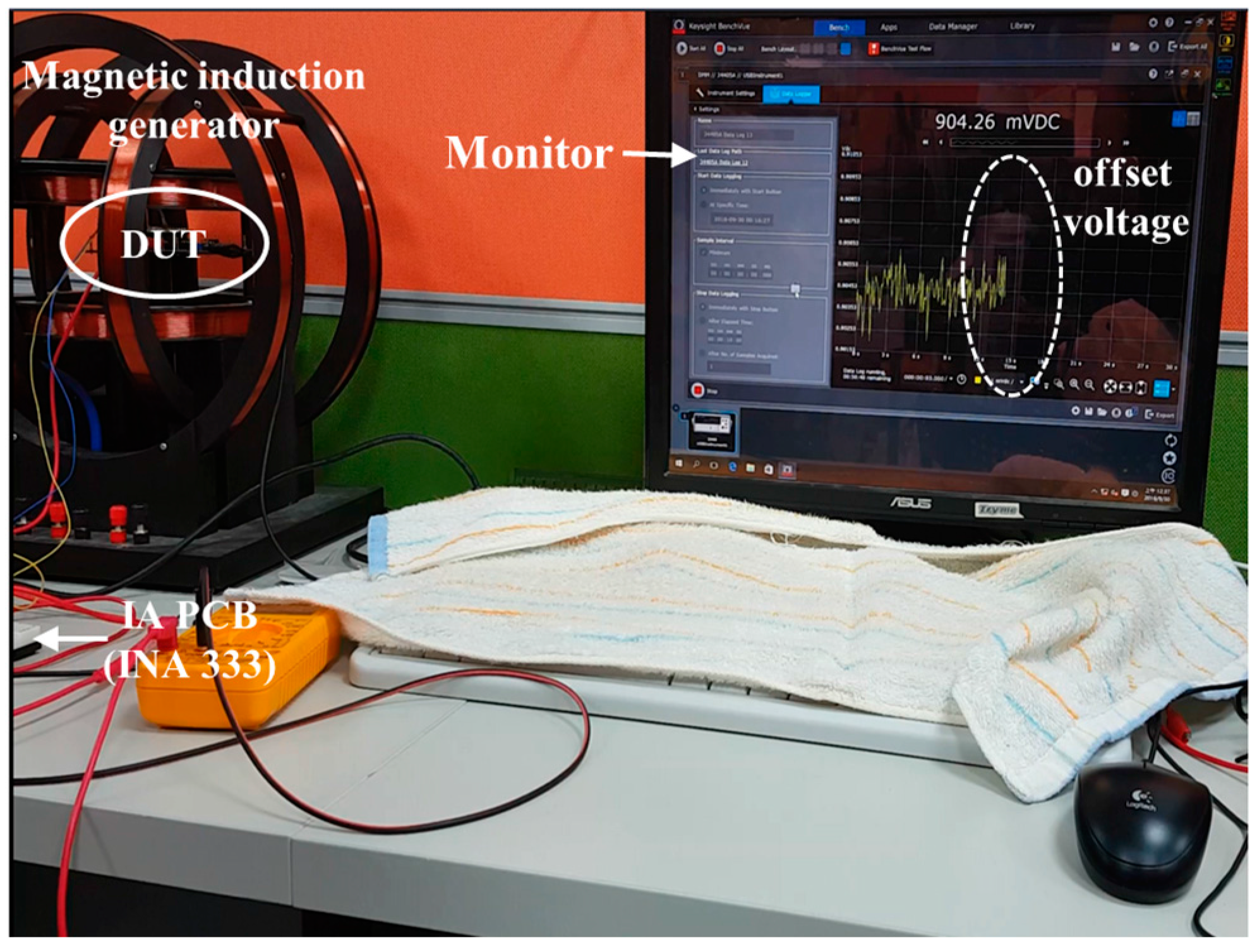
Figure 4 presents the experimental setup of the distance detector composed of a device under test (DUT), an IA (INA333, Texas Instruments, Dallas, TX, USA) printed circuit board (PCB), a digital multimeter (Agilent 34405A, Santa Clara, CA, USA), a magnetic body (human), and a power regulator with a 9-V battery. The DUT included the strip MAGFET and readout circuit, and the magnetic body was actually a human weighing approximately 65 kg. The distance was defined from the chip center of the DUT to the weight center of the magnetic body. Notably, the proposed distance detecting method is not only a universal detection method but also operates in dark conditions away from light emission. To enhance the sensitivity of the distance detection and to increase the detecting distance, a commercial IA (INA333) was applied to amplify the output voltage of the readout circuit.
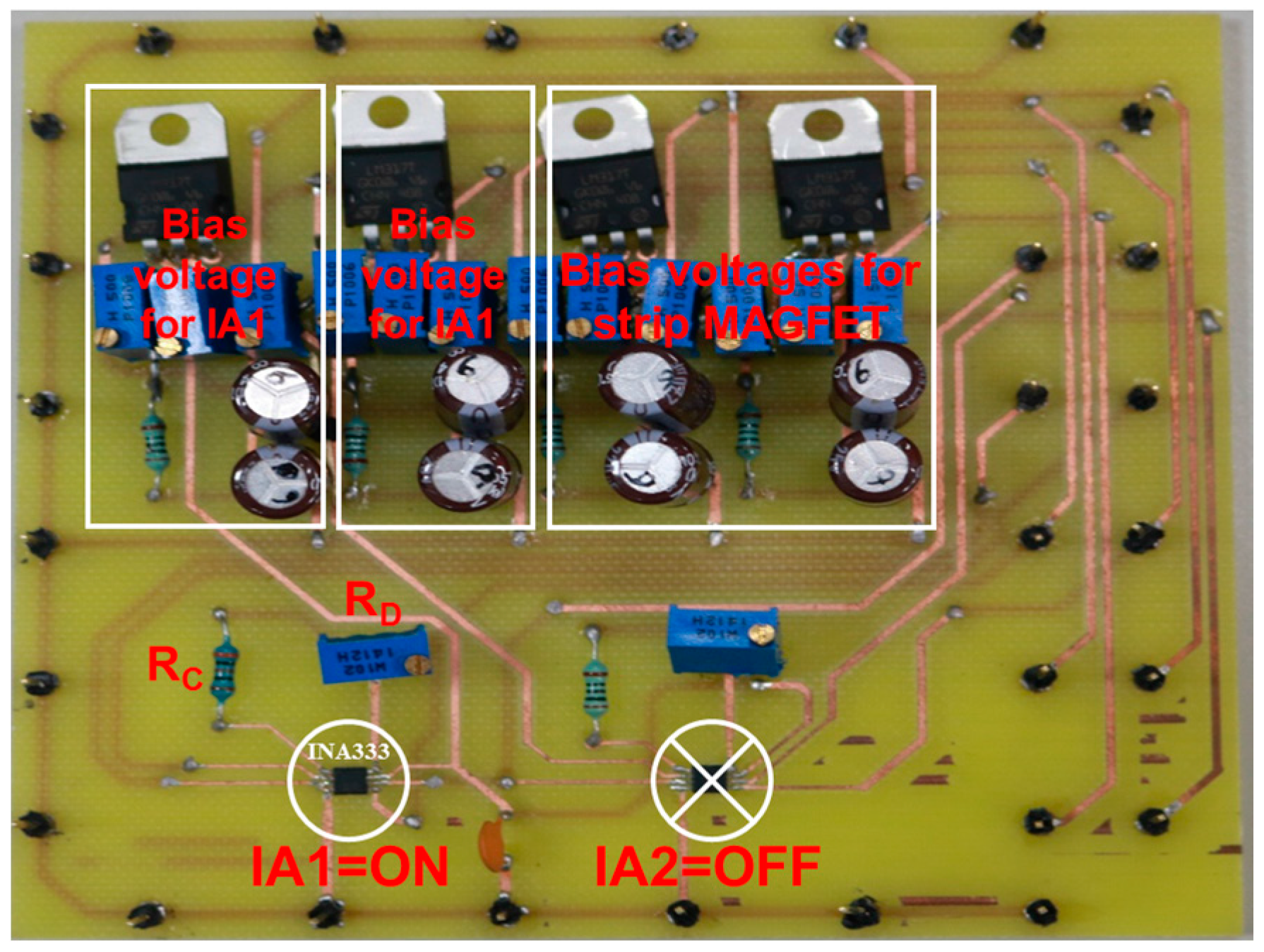
Figure 5 presents the applied PCB that includes two commercial IAs, two bias voltages for IAs, two bias voltages for the proposed strip MAGFET, and resistors,
RC and
RD. By adjusting the variable resistor
RD, the magnifying power of IA1 was set to 43 dB (approximately 150 times).
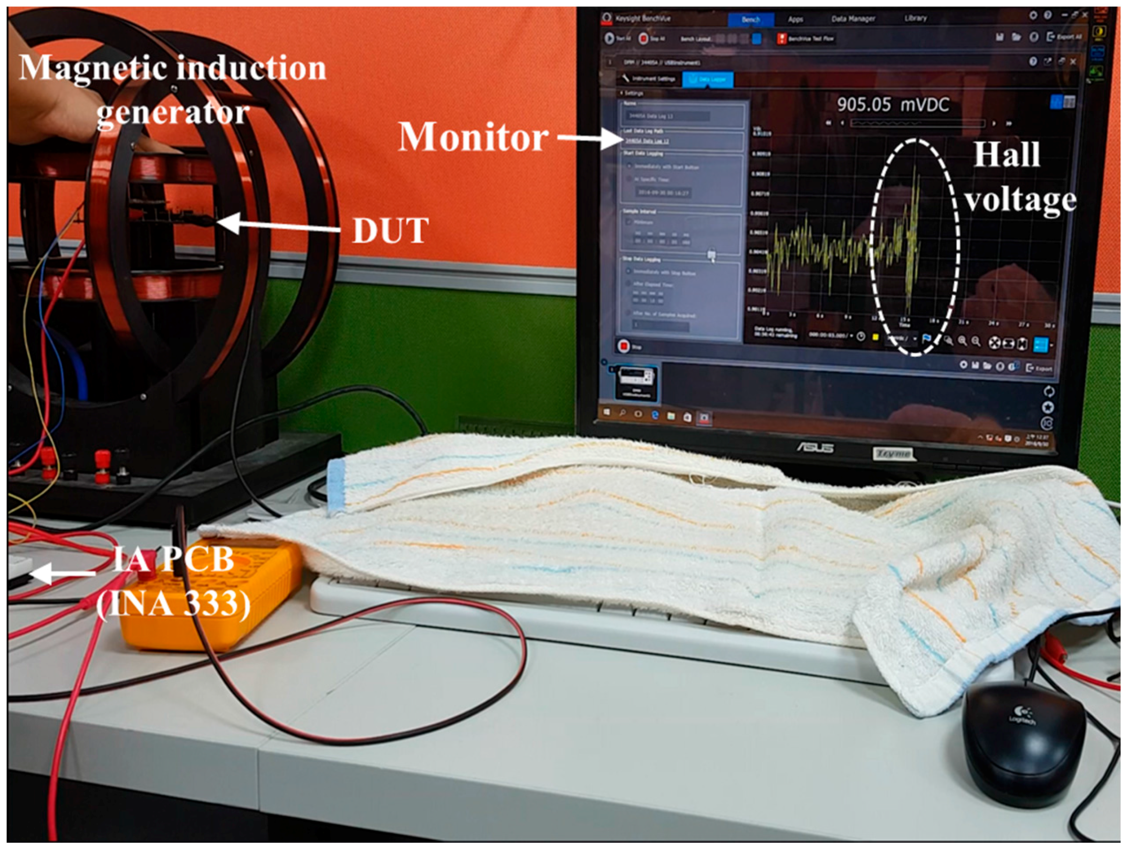
Figure 6 and
Figure 7 present the measured equipment that includes a magnetic induction generator, a commercial IA (INA333) PCB, and a display monitor. As shown in
Figure 6, only the offset voltage was displayed on the monitor and not the magnetic body. When the magnetic body contacts with the distance detector, Hall voltage evidently appeared on the monitor, as shown in
Figure 7. A quality analysis of the measured Hall voltage is presented in
Figure 7. To avoid bias, a digital multimeter (Agilent 34405A) was used for the quantity analysis of the distance detector that included a strip MAGFET, readout circuit, and IA PCB (INA333).
4. Simulated and Measured Results
This paper presents a low-voltage two-stage cascaded opamp with Miller compensation and compact class-AB output stage based on 0.18 μm CMOS technology for distance detection [
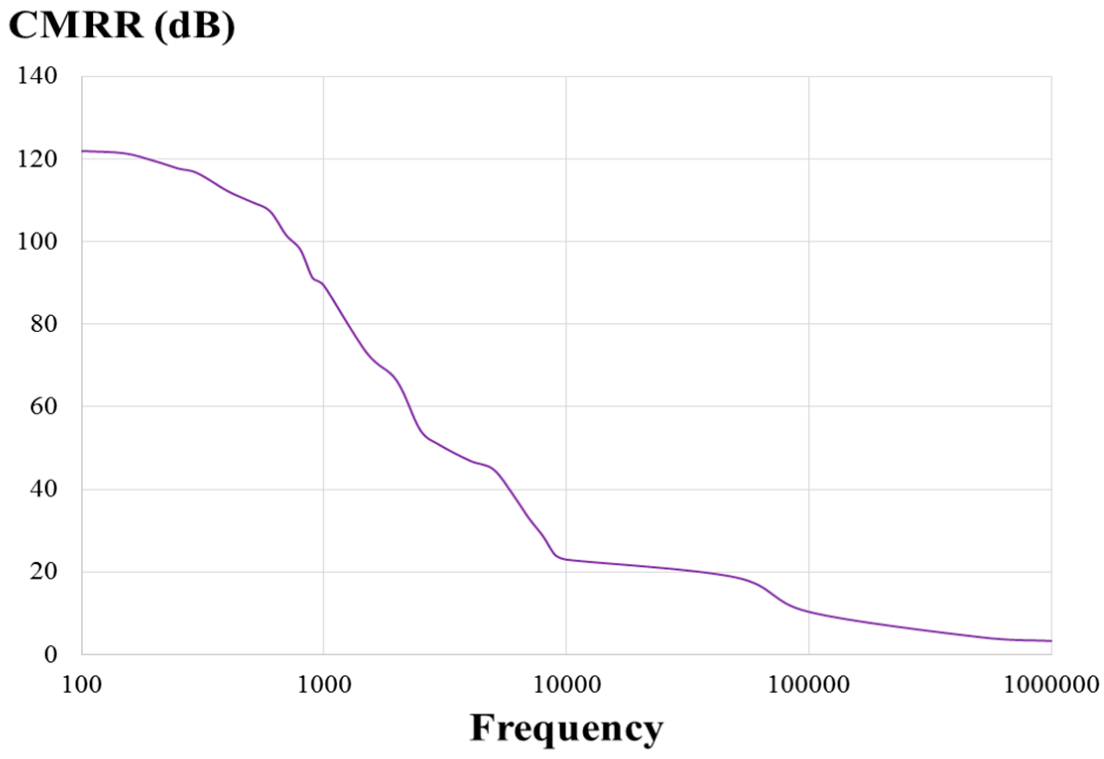
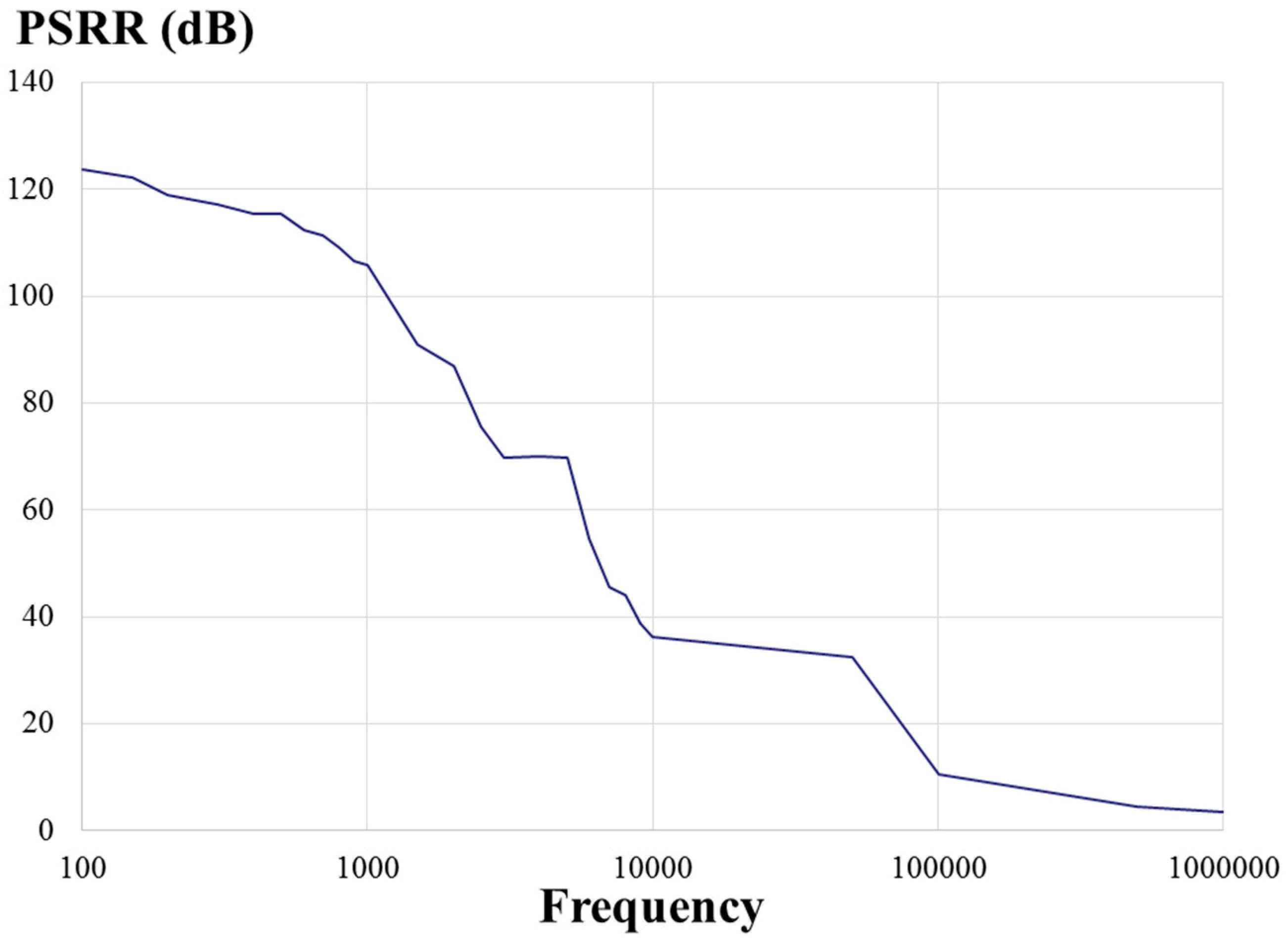
25]. The simulated results demonstrated that the designed two-stage cascaded opamp had an open-loop gain of 75.3 dB, a phase margin of 54.9°, a common-mode rejection ratio (CMRR) of 123 dB, a slew rate of 0.07 V/μs, an input common-mode range (ICMR) of 0.9 V, a power supply rejection ratio (PSRR) of 119 dB, an output swing of 1.70 V, power consumption of 179 μW for a power supply of 1.8 volts, and a load capacitor of 10 pF.
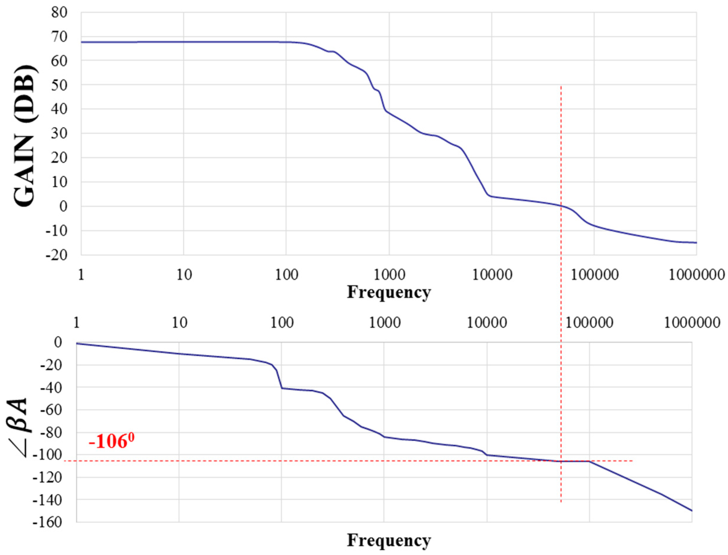
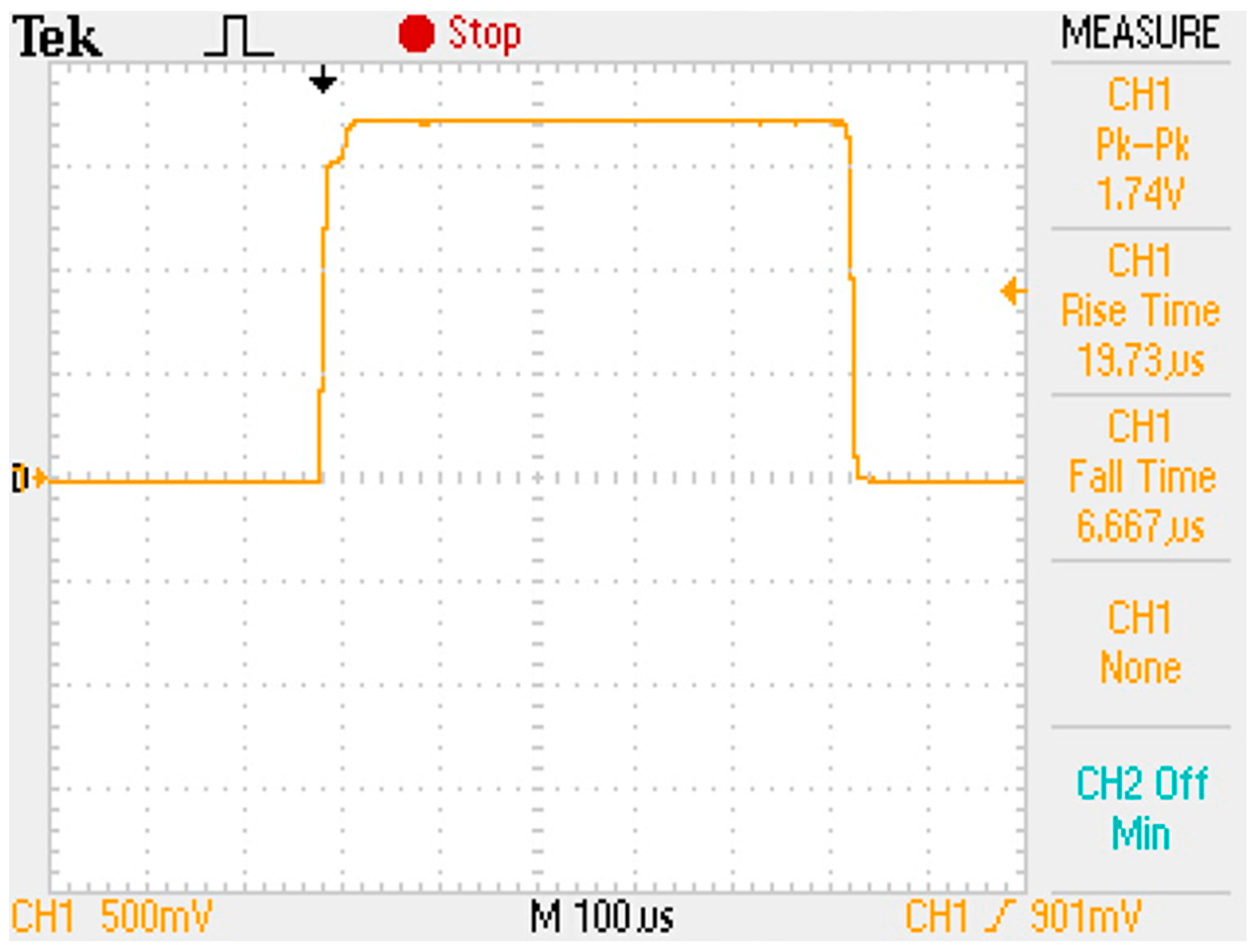
Figure 8 presents a measured open-loop gain of 67.7 dB and phase of 74° with respect to frequency. The measured open-loop gain was lower than that obtained through simulation, but the measured phase was higher than that obtained through simulation.
Figure 9 and
Figure 10 present the measured CMRR and PSRR, respectively, which were approximately equal to the relative simulated results. Furthermore,
Figure 11 presents a measured slew rate of 0.07 V/μs, rise time of 19.73 μs, and fall time of 6.67 μs at an operating frequency of 1 kHz. The simulated and measured results compared with those of previous studies are tabulated in
Table 1. Measured results of voltage gain, phase margin, CMRR, slew rate, ICMR, PSRR, and output swing, were more favorable than those obtained in previous studies [
26,
27]. Although these previous studies have not proved the efficiency, the measured data in the present study verified that the designed opamp worked as intended.
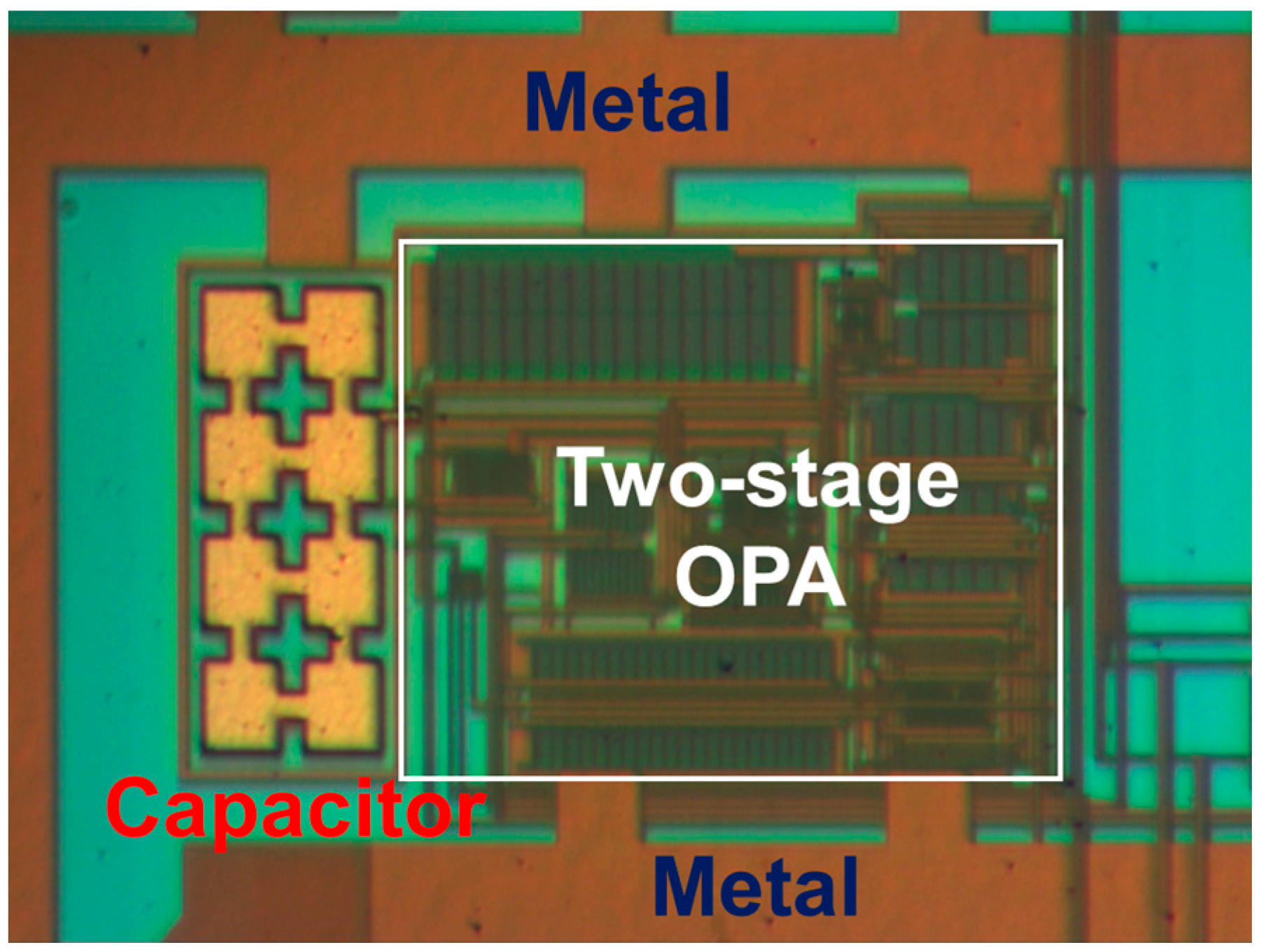
Figure 12 presents the microphotograph of the designed opamp without external resistors and capacitors. Notably, an output voltage
VOUT was acquired at the output node of the DA by multiplying the drain current difference ∆
ID with external resistors,
RA = 100 kΩ and
RB = 6.2 kΩ. That is, the voltage gain of the DA was approximately 17 times greater.
To elucidate the detection mechanism, the experimental setup can be divided into three categories: direct measurement without grounding (direct), grounding to earth with electrostatic discharge (ESD) wrist strap (Strap E-GND), and grounding to power supply with ESD wrist strap (Strap S-GND). The first category elucidates the influence of ESD without grounding. Next, ESD will be eliminated from the magnetic sensor by grounding it to earth. Finally, in the third category, the ESD wrist strap is grounded to the power supply, and not to earth. This connection will enable the removal of ESD from the magnetic sensor to the power supply; however, ESD always exists between the power supply and earth.
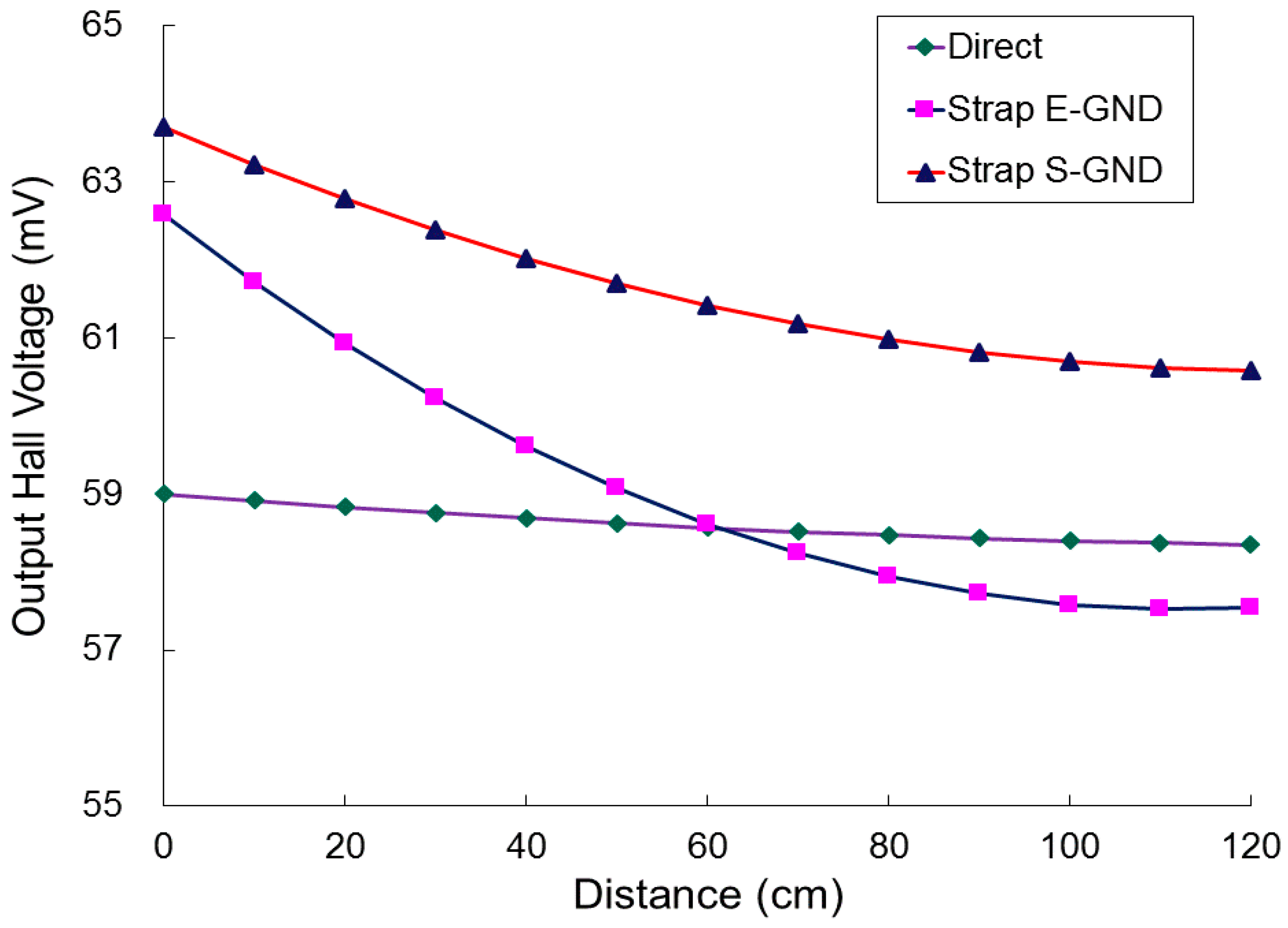
Figure 13 presents the measured output Hall voltages as a function of the distance, from 0 cm to 120 cm in steps of 10 cm, at a CSHP bias current (
Ibias) of 12 mA. In the first category, the measured output Hall voltage varied from 58.35 to 59.00 mA. The voltage variation was approximately 0.65 mV. In the second category, the variation in the measured output Hall voltage was approximately 5.04 mV, from 57.54 to 62.58 mV. In the third category, the variation in the measured output Hall voltage was approximately 3.12 mV, from 60.58 to 63.70 mV. According to the measured Hall voltage, the second category performed with a more efficient sensitivity than the other two, and the first category performed with minimum sensitivity of nearly zero. That is, ESD could be eliminated from the magnetic sensor by grounding it to earth; however, ESD will cancel the sensitivity out when the sensor is not grounded. Notably, saturation was observed in the second category. This result indicates that the magnetic influence can be ignored if the human stayed far from the DUT, which was grounded to earth by using the ESD wrist strap (Strap E-GND). However, the first and third categories were still influenced by the magnetic body (human). Both ‘no grounding’ and ‘grounding to power supply’ were unsuitable for measuring the induced Hall voltage although the magnetic body was far and away from the designed DUT.
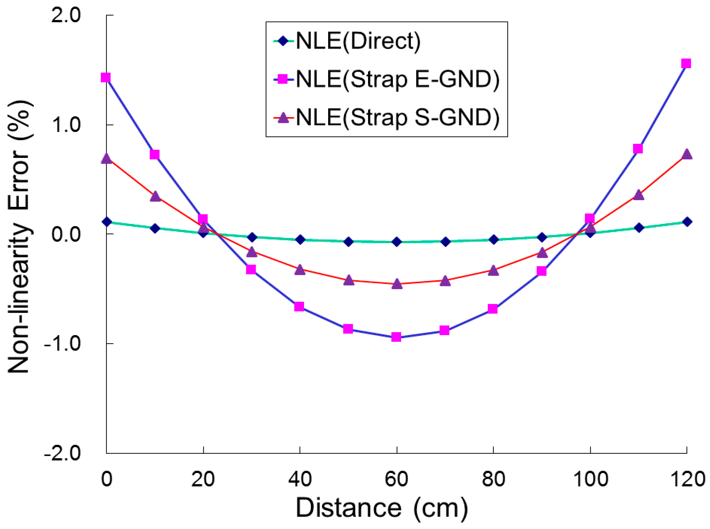
Figure 14 presents the measured
NLE as a function of distance, from 0 to 120 cm in steps of 10 cm, and various categories for the designed strip MAGFET with a readout circuit and an IA PCB. The variation in
NLE was large when the MAGFET was operated in category 2 conditions in which the measurement is completed by grounding the sensor to earth with an ESD wrist strap (Strap E-GND).
NLE was nearly constant when the measurement was finished without grounding. The sensor performed with a linear characteristic when operated in category 1, but yielded a quadratic curve in categories 2 and 3. Notably,
NLE was equal to zero at two distances, 20 and 100 cm. The measured output voltage difference ∆
VOUT was equal to the calculated output voltage difference ∆
V(0)OUT on the basis of the slope of the straight line obtained from the best fit to the output characteristic [
24].
Table 2 summarizes the measured results of the proposed strip MAGFET with a readout circuit and an IA PCB (INA333). The average nonlinearity
NLEave and the maximum nonlinearity
NLEmax were proportional to the measured Hall voltage difference ∆
VH and the current-related sensitivity
SRI(
D) with a bias current of 12 mA. The maximum current-related magnetosensitivity was 0.35 V/A·m at an output Hall voltage of 5.04 mV and a distance of 0 cm (i.e., the magnetic body contacts with DUT). The measured results demonstrated that the proposed strip MAGFET was an effective distance sensor; however, it presented poor linearity.
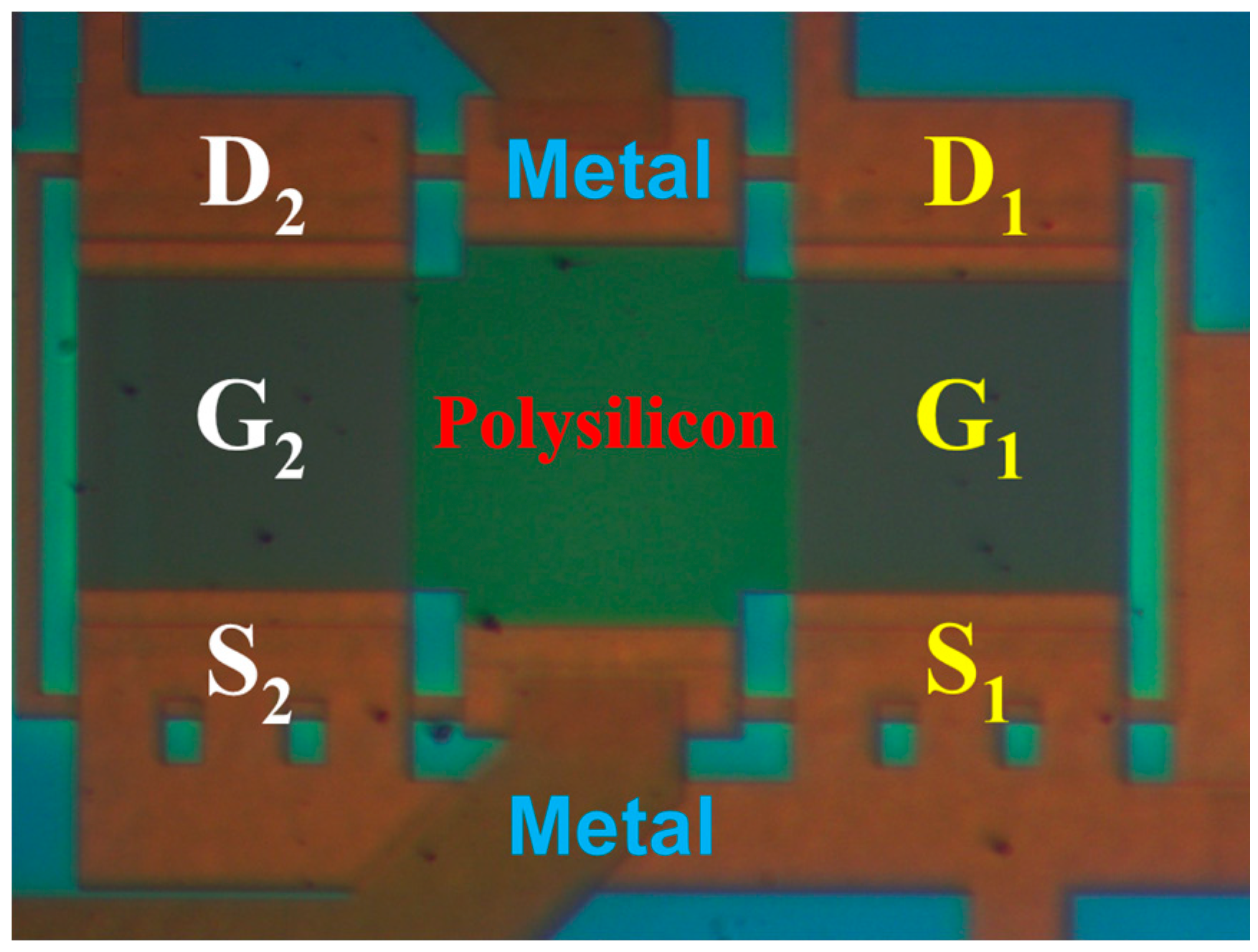
Figure 15 presents a microphotograph of the proposed strip MAGFET with a chip area of approximately 100 × 220 μm
2.


