
Large Out-of-Plane Displacement Bistable Electromagnetic Microswitch on a Single Wafer

Abstract
:1. Introduction
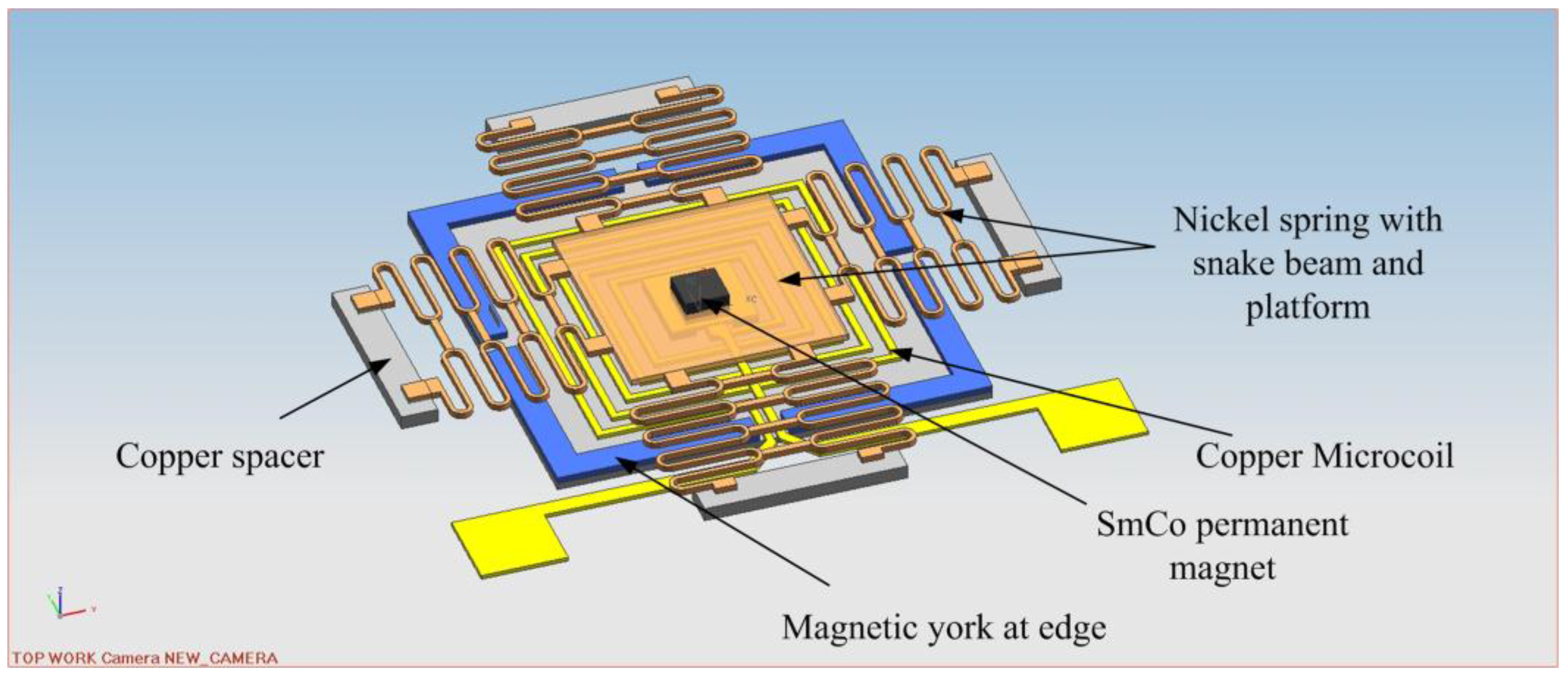
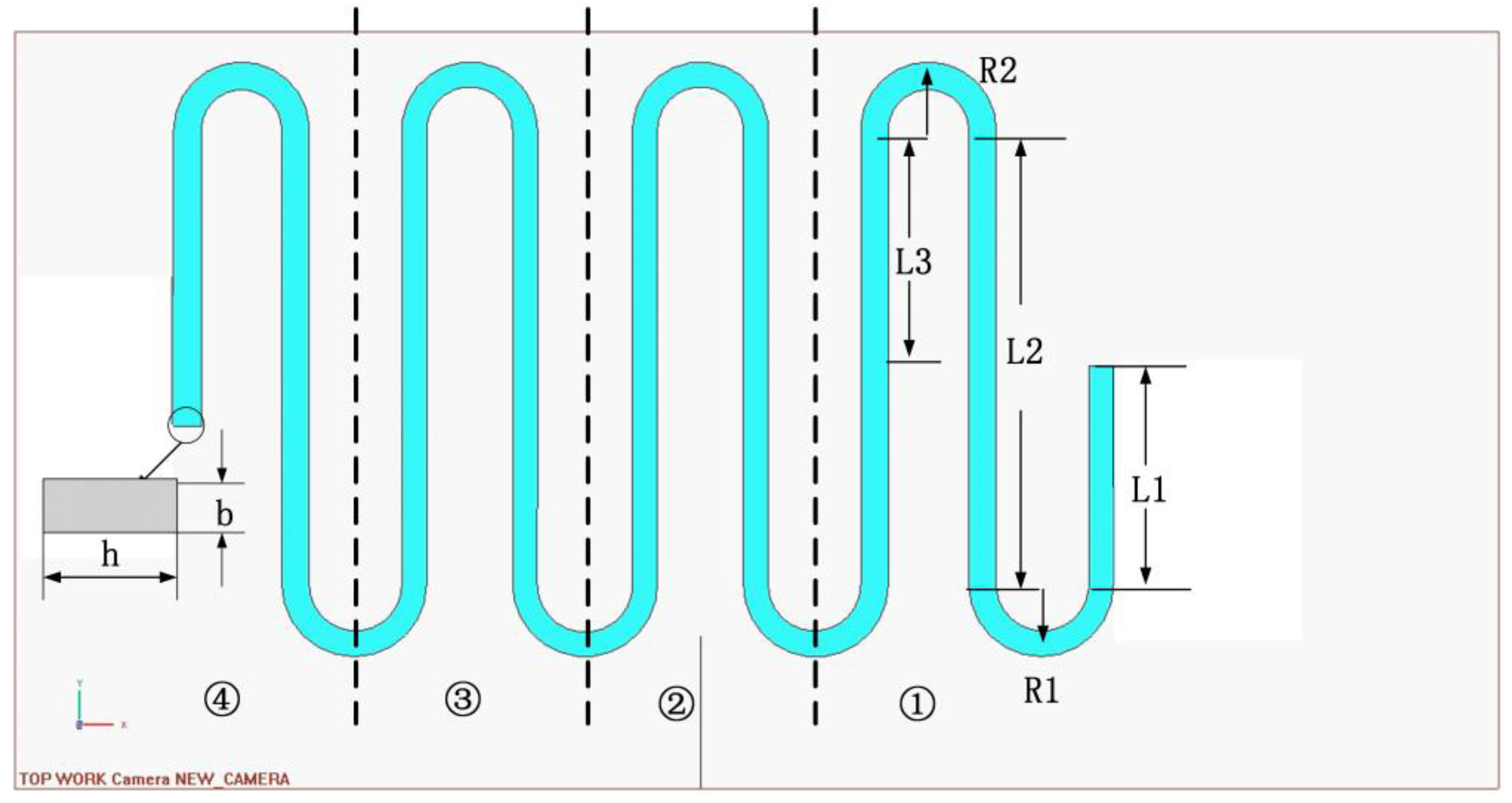
2. Design of the Microswitch
3. Analysis and Simulation of the Mechanical Force of the Spring
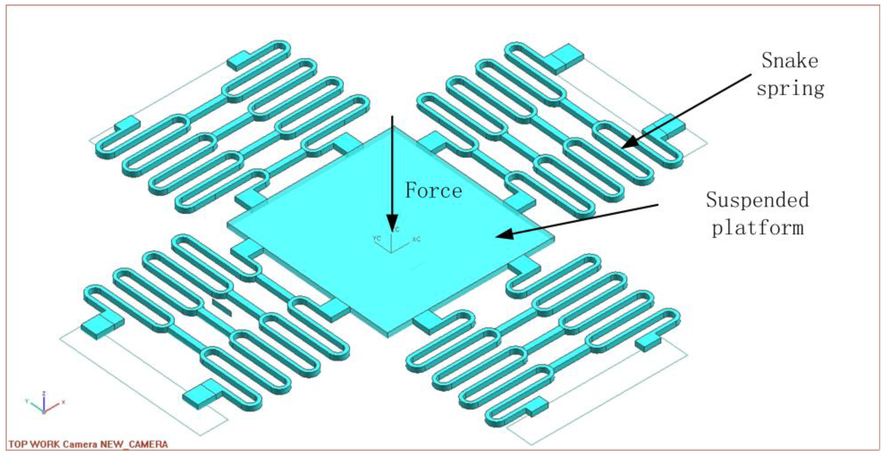
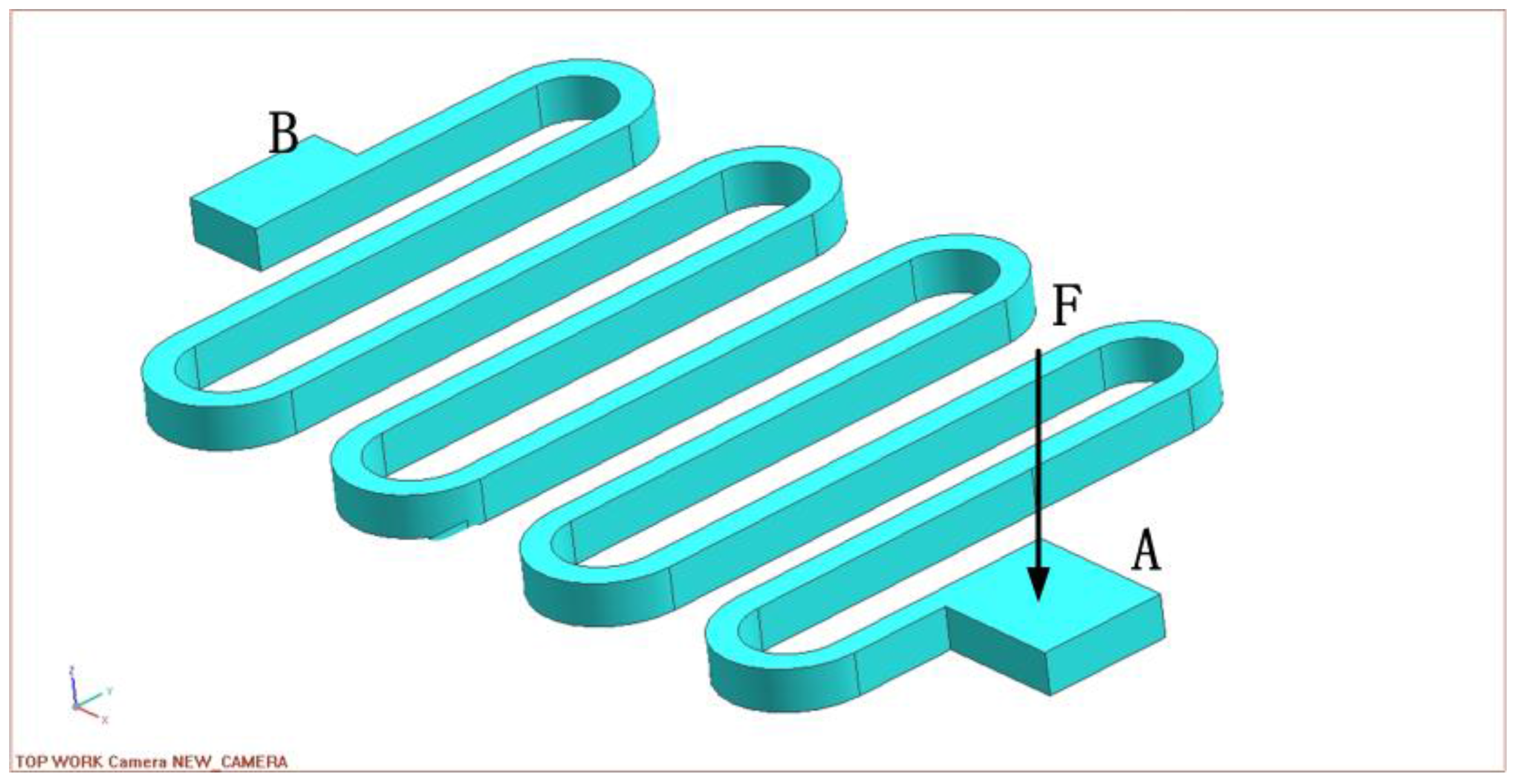
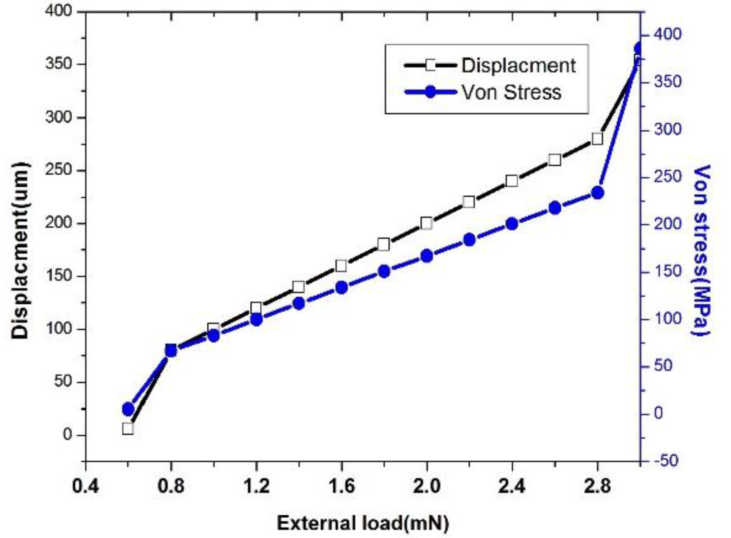
3.1. Theory Analysis
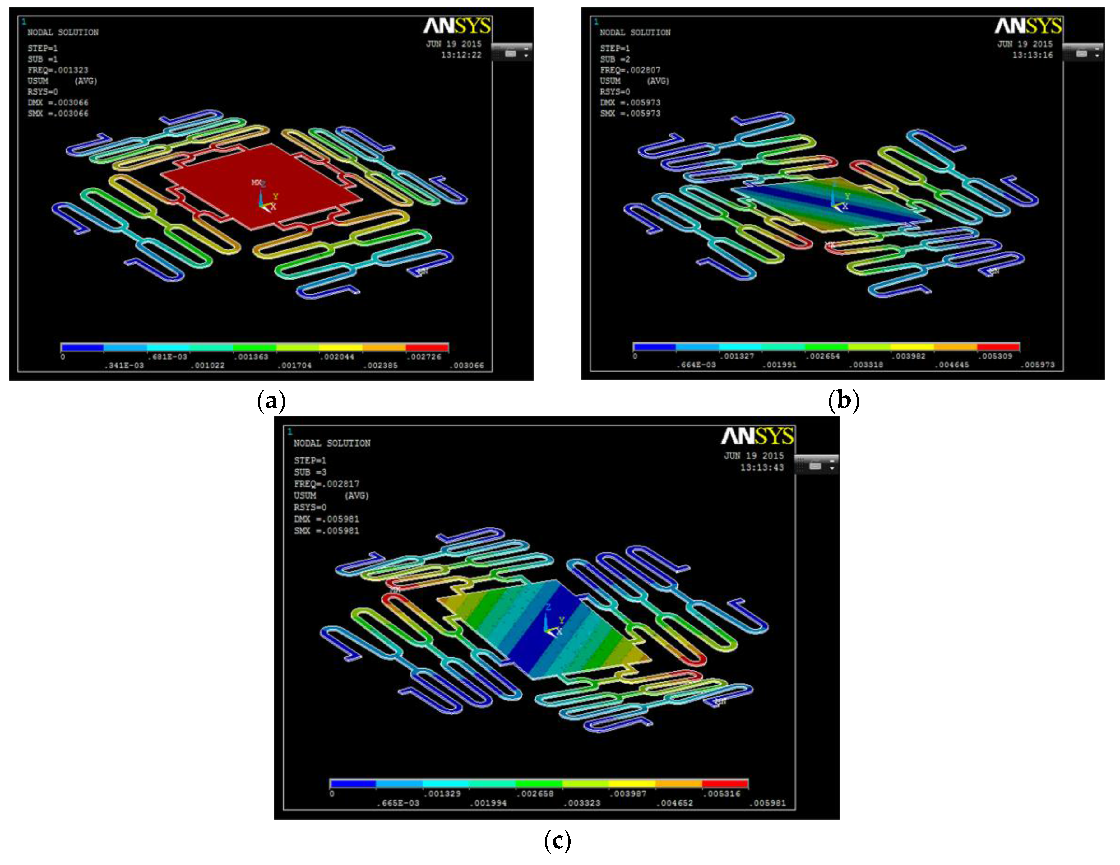
3.2. Finite Element Analysis
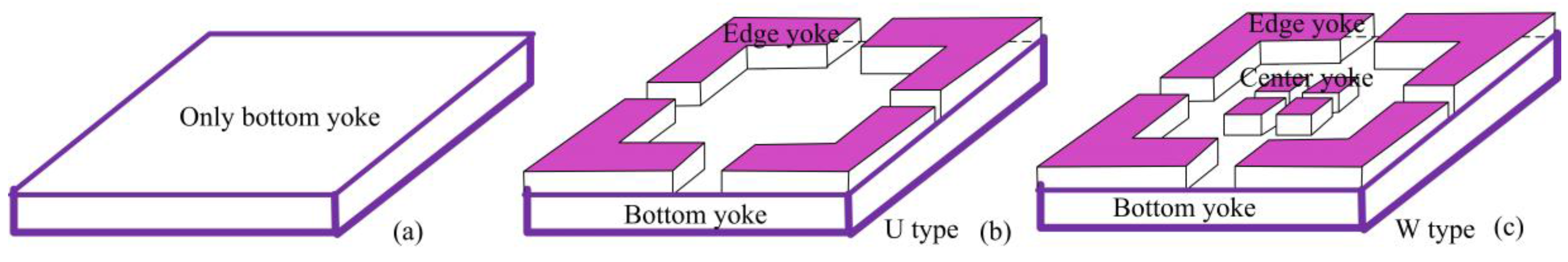
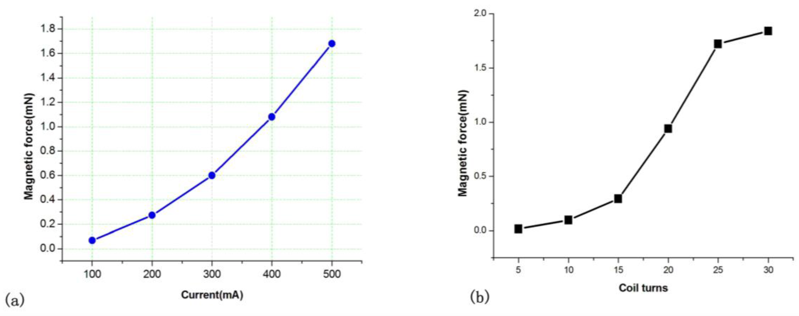
4. Analysis and Simulation of the Magnetic Force
4.1. Theory Analysis
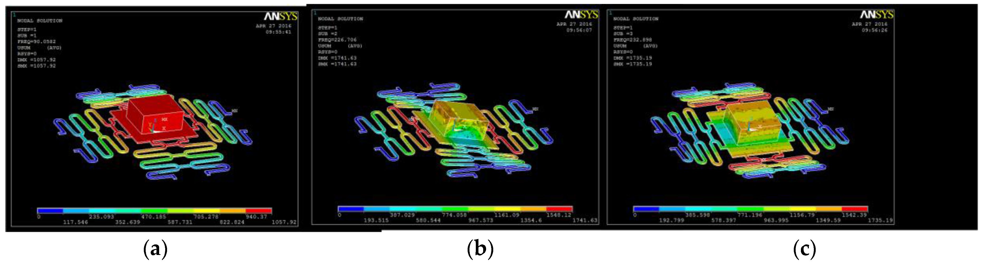
4.2. Finite Element Simulation
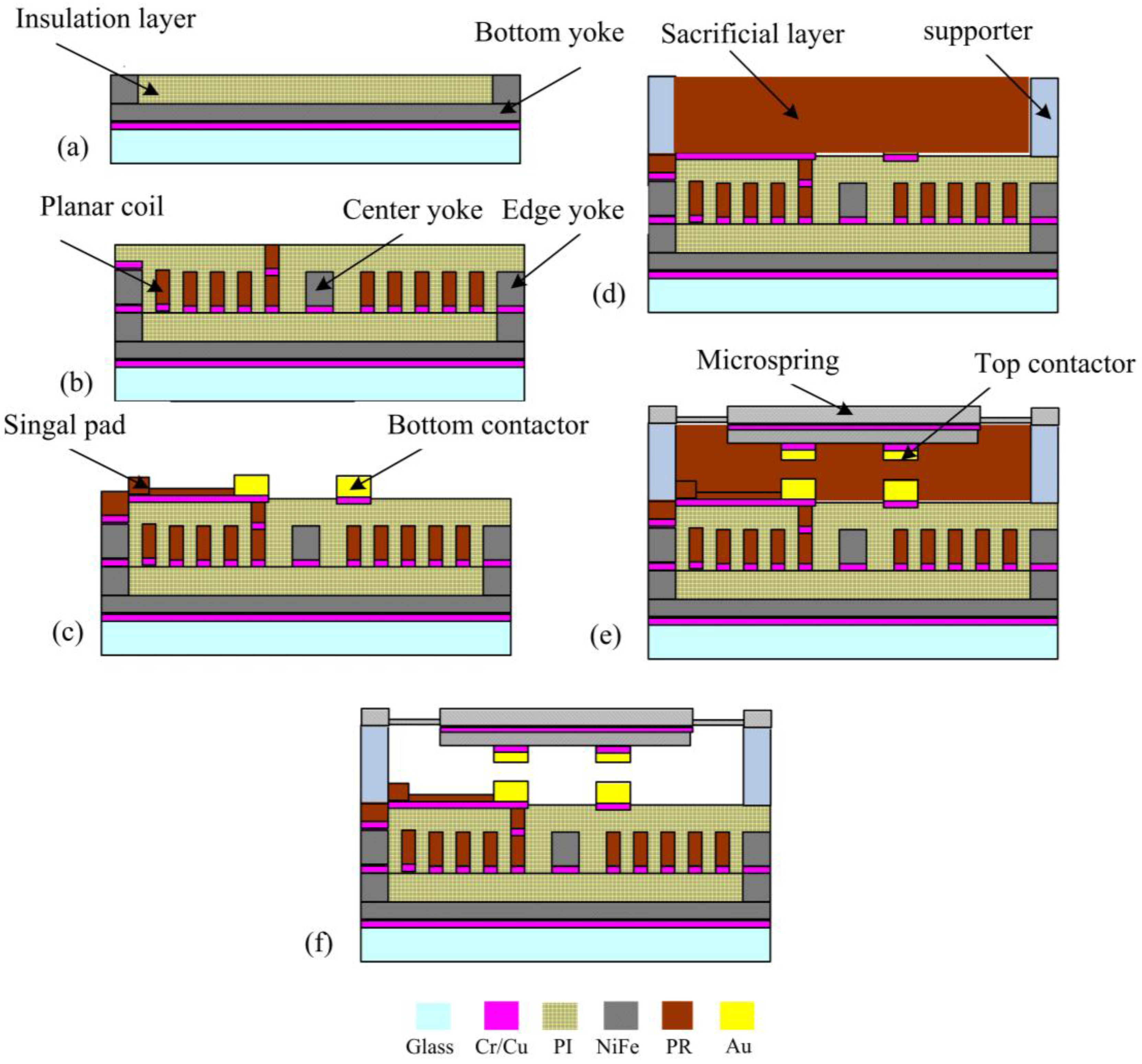
5. Microfabrication
- (a)
- Chromium/copper (Cr/Cu) was sputtered as the seed layer for plating of the device structure, then, the photoresist spin-coating and photoresist were carried out. The bottom magnetic yoke was created by electroplating the permalloy. After stripping the photoresist, the exposed seed layer was wet etched. Then, the polyimide was spin coated, thermal treated and planarized as insulation layer.
- (b)
- After secondly sputtering the Cr/Cu seed layer and spin-coating photoresist, the microcoil, via connection and one pad was created by photolithography and electroplating copper. After stripping the photoresist and wet etching the exposed seed layer, the polyimide layer was spin coated, thermally treated, and planarized.
- (c)
- The signal lines were created by spin-coating photoresist, photolithography, and electroplating copper after sputtering the Cr/Cu seed layer. Then the contactor on the signal line was formed by photolithography, and electroplating copper, nickel, and gold in sequence.
- (d)
- Two layers of 80 μm thick photoresist was spin coated and thermally treated step-by-step as sacrificial material. Then the nickel supporter was electroplated with high aspect ratio structure after photolithography.
- (e)
- The top contactors were formed by photolithography and electroplating gold, nickel, copper in sequence after sputtering Cr/Cu seed layer. Then the next Cr/Cu seed layer was sputtered, the photoresist was spin coated and the microspring was formed by photolithography, and electroplating permalloy, nickel step by step.
- (f)
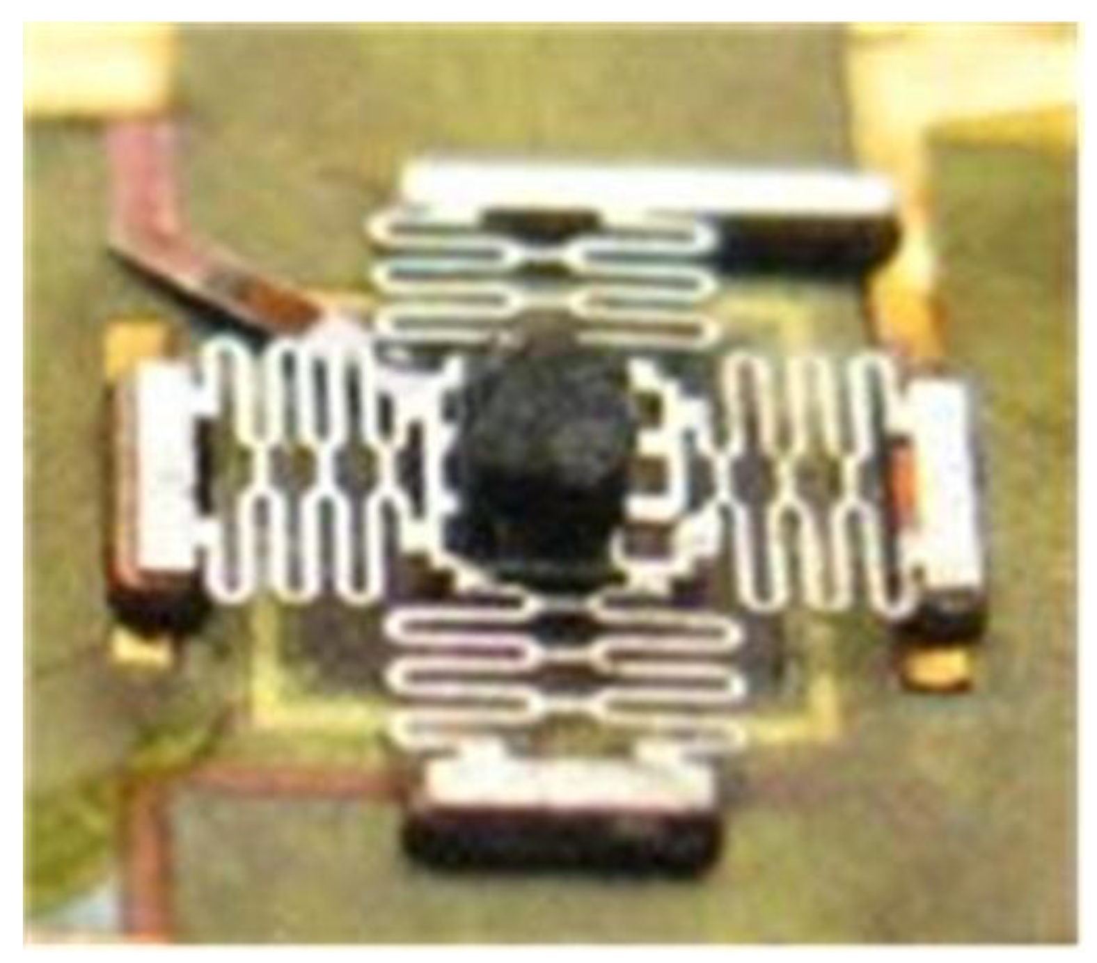
- The thick photoresist sacrificial layer underneath microspring was released in 2 wt % NaOH solution layer by layer and Cu seed layer was wet etched in ammonia solution with assistance of hydrogen peroxide and seed Cr layer was etched by an improved oxidizer etching solution. In order to avoid sticking, the wafer was immersed in ethyl alcohol for rapid evaporation to form the suspended microspring. Finally, the permanent magnet was assembled on the center of the microspring. The fabricated prototype was shown in Figure 11.
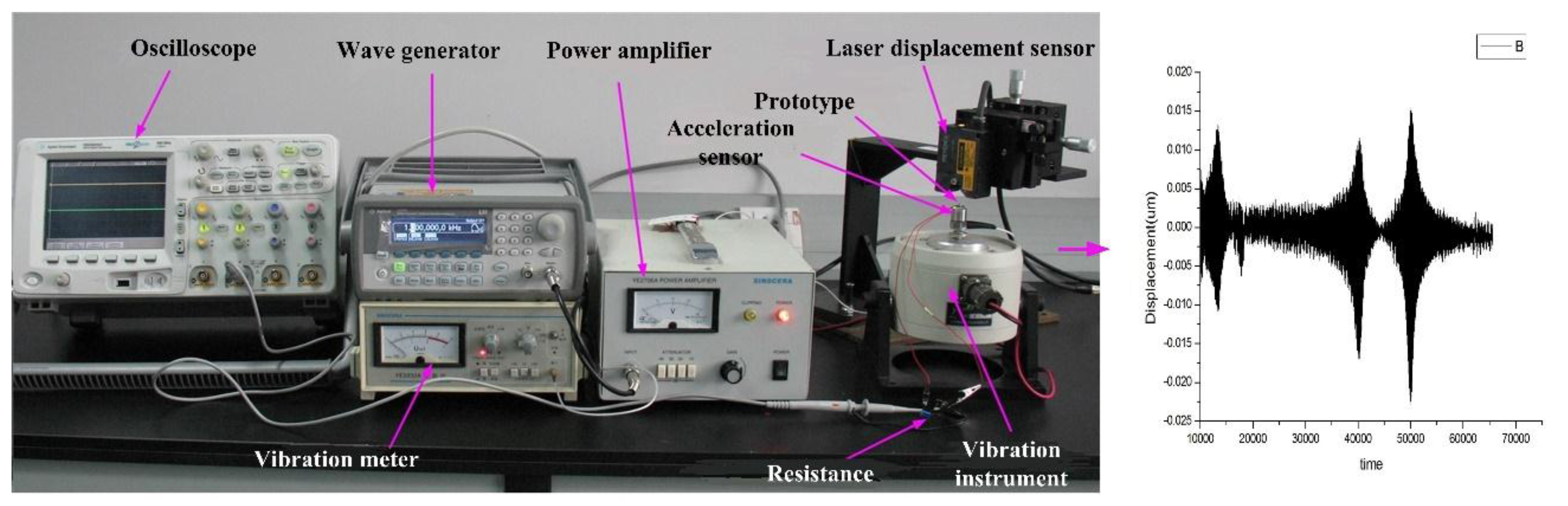
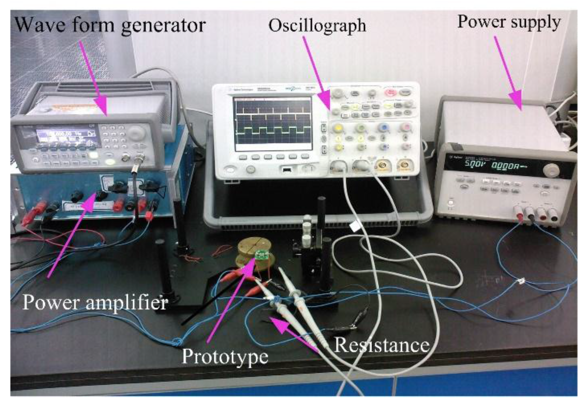
6. Characterization
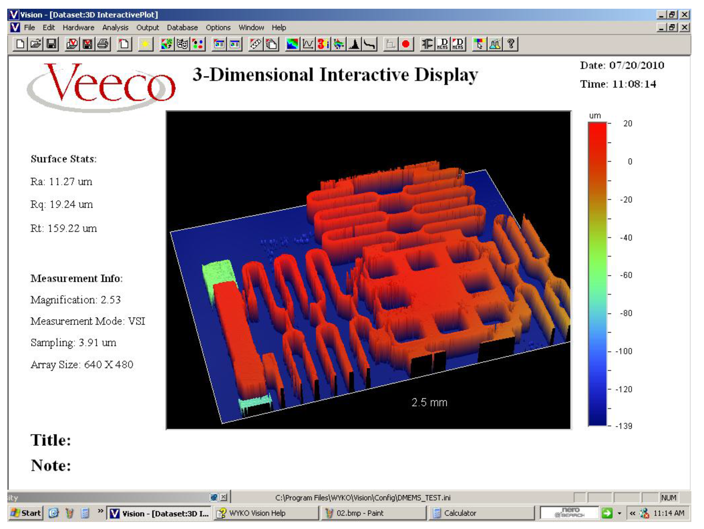
6.1. Static Surface
6.2. Dynamic Response Testing
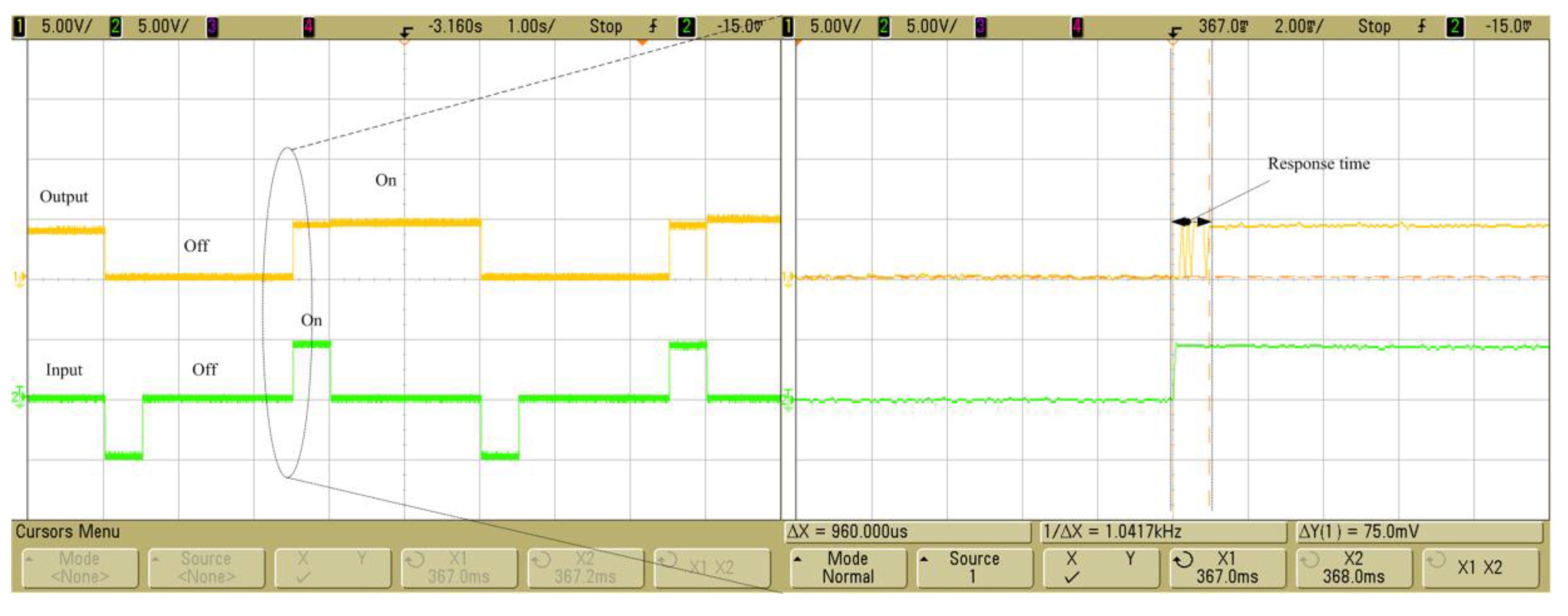
6.3. Bistable Mechanism Test
7. Conclusions
Acknowledgments
Author Contributions
Conflicts of Interest
References
- Bao, M.; Wang, W. Future of micro-electromechanical systems. Sens. Actuators A Phys. 1996, 56, 135–141. [Google Scholar] [CrossRef]
- Marinis, T.F. The Future of microelectromechanical systesms (MEMS). Strain 2009, 45, 208–220. [Google Scholar] [CrossRef]
- Judy, J.W. Microelectromechanical systems (MEMS): Fabrication, design and applications. Smart Mater. Struct. 2001, 10, 1115–1134. [Google Scholar] [CrossRef]
- Wu, L.; Xie, H.K. A large vertical displacement electrothermal bimorph microactuator with very small lateral shift. Sens. Actuators A Phys. 2008, 145, 371–379. [Google Scholar] [CrossRef]
- Bazaz, S.A.; Khan, F.; Shakoor, R.I. Design, simulation and testing of electrostatic SOI MUMPs based microgripper integrated with capacitive contact sensor. Sens. Actuators A Phys. 2011, 167, 44–53. [Google Scholar] [CrossRef]
- Jaafar, H.; Beh, K.S.; Yunus, N.A.M.; Hasan, W.Z.W.; Shafie, S.; Sidek, O. A comprehensive study on RF MEMS switch. Microsyst. Technol. 2014, 20, 2109–2121. [Google Scholar] [CrossRef]
- Wang, Y.; Li, Z.; McCormick, D.T.; Tien, N.C. A micromachined RF microrelay with electrothermal actuation. Sens. Actuators A Phys. 2003, 103, 231–236. [Google Scholar] [CrossRef]
- Cugat, O.; Delamare, J.; Reyne, G. Magnetic micro-actuators and systems. (MAGMAS). IEEE Trans. Magn. 2010, 39, 3607–3612. [Google Scholar] [CrossRef]
- Solgaard, O.; Godil, A.A.; Howe, R.T.; Lee, L.P.; Peter, Y.A.; Zappe, H. Optical MEMS: From micromirrors to complex systems. J. Microelectromech. Syst. 2014, 23, 517–538. [Google Scholar] [CrossRef]
- Kim, Y.S.; Dagalakis, N.G.; Gupta, S.K. Creating large out-of-plane displacement electrothermal motion stage by incorporating beams with step features. J. Micromech. Microeng. 2013, 23, 055008–055010. [Google Scholar] [CrossRef]
- Seki, T.; Uno, Y.; Narise, K.; Masuda, T.; Inoue, K.; Sato, S.; Sato, F.; Imanaka, K.; Sugiyama, S. Development of a large-force low-loss metal-contact RF MEMS switch. Sens. Actuators A Phys. 2006, 132, 683–688. [Google Scholar] [CrossRef]
- Han, J.S.; Ko, J.S.; Korvink, J.G. Structural optimization of a large-displacement electromagnetic Lorentz force microactuator for optical switching applications. J. Micromech. Microeng. 2004, 14, 1585–1596. [Google Scholar] [CrossRef]
- Lv, X.; Wei, W.; Mao, X.; Chen, Y.; Yang, J.; Yang, F. A novel MEMS electromagnetic actuator with large displacement. Sens. Actuators A Phys. 2015, 221, 22–28. [Google Scholar] [CrossRef]
- Glickman, M.; Tseng, P.; Harrison, J.; Niblock, T.; Goldberg, I.B.; Judy, J.W. high-performance lateral-actuating magnetic MEMS switch. J. Microelectromech. Syst. 2011, 20, 842–851. [Google Scholar] [CrossRef]
- Sawant, S.G.; Wang, N.; Hanna, M.S.; Taylor, C.R.; Arnold, D.P. Fabrication, characterizaiton, and modeling of fully-batch-fabricated pistion-type electrodynamic microactuators. J. Microelectromech. Syst. 2014, 23, 220–229. [Google Scholar] [CrossRef]
- Gray, G.D., Jr.; Kohl, P.A. Magnetically bistable actuator Part 1. Ultra-low switching energy and modeling. Sens. Actuators A Phys. 2005, 119, 489–501. [Google Scholar] [CrossRef]
- Gray, G.D., Jr.; Kohl, P.A. Magnetically bistable actuator Part 2. Fabrication and performance. Sens. Actuators A Phys. 2005, 119, 502–511. [Google Scholar] [CrossRef]
- Williams, J.D.; Yang, R.; Wang, W. Numerical simulation and test of a UV-LIGA-fabricated electromagnetic micro-relay for power applications. Sens. Actuators A Phys. 2005, 120, 154–162. [Google Scholar] [CrossRef]
- Fu, S.; Ding, G.; Wang, H.; Yang, Z.; Feng, J. Design and fabrication of a magnetic bi-stable electromagnetic MEMS relay. Microelectron. J. 2007, 38, 556–563. [Google Scholar] [CrossRef]
- Hartley, A.C.; Miles, R.E.; Corda, J.; Dimitrakopoulos, N. Large throw magnetic microactuator. Mechtronics 2008, 18, 459–465. [Google Scholar] [CrossRef]
- Miao, X.; Dai, X.; Huang, Y.; Ding, G.; Zhao, X. Segmented magnetic circuit simulation of the large displacement planar micro-coil actuator with enclosed magnetic yokes. Microelectron. Eng. 2014, 129, 38–45. [Google Scholar] [CrossRef]


| m = b/h | 1.0 | 1.2 | 1.5 | 2.0 | 2.5 | 3.0 | 4.0 | 6.0 | 8.0 |
|---|---|---|---|---|---|---|---|---|---|
| 0.140 | 0.199 | 0.294 | 0.457 | 0.622 | 0.790 | 1.123 | 1.789 | 2.456 |
| Elastic Modulus | 210 GPa |
|---|---|
| Passion ration | 0.3 |
| Density | 8.96 kg/cm3 |
| Name | Value (μm) |
|---|---|
| L1 | 190 |
| L2 | 520 |
| R | 83 |
| H | 31 |
| n | 15 |
| Magentic Yoke | Bottom Yoke (a) | U Yoke (b) | W Yoke (c) |
|---|---|---|---|
| Magnetic force (mN) | 0.23 | 1.36 | 1.68 |
© 2016 by the authors; licensee MDPI, Basel, Switzerland. This article is an open access article distributed under the terms and conditions of the Creative Commons Attribution (CC-BY) license (http://creativecommons.org/licenses/by/4.0/).
Share and Cite
Miao, X.; Dai, X.; Huang, Y.; Ding, G.; Zhao, X. Large Out-of-Plane Displacement Bistable Electromagnetic Microswitch on a Single Wafer. Sensors 2016, 16, 634. https://doi.org/10.3390/s16050634
Miao X, Dai X, Huang Y, Ding G, Zhao X. Large Out-of-Plane Displacement Bistable Electromagnetic Microswitch on a Single Wafer. Sensors. 2016; 16(5):634. https://doi.org/10.3390/s16050634
Chicago/Turabian StyleMiao, Xiaodan, Xuhan Dai, Yi Huang, Guifu Ding, and Xiaolin Zhao. 2016. "Large Out-of-Plane Displacement Bistable Electromagnetic Microswitch on a Single Wafer" Sensors 16, no. 5: 634. https://doi.org/10.3390/s16050634