
Fast Industrial Inspection of Optical Thin Film Using Optical Coherence Tomography

 ,
, 
Abstract
:1. Introduction
2. Materials and Methods
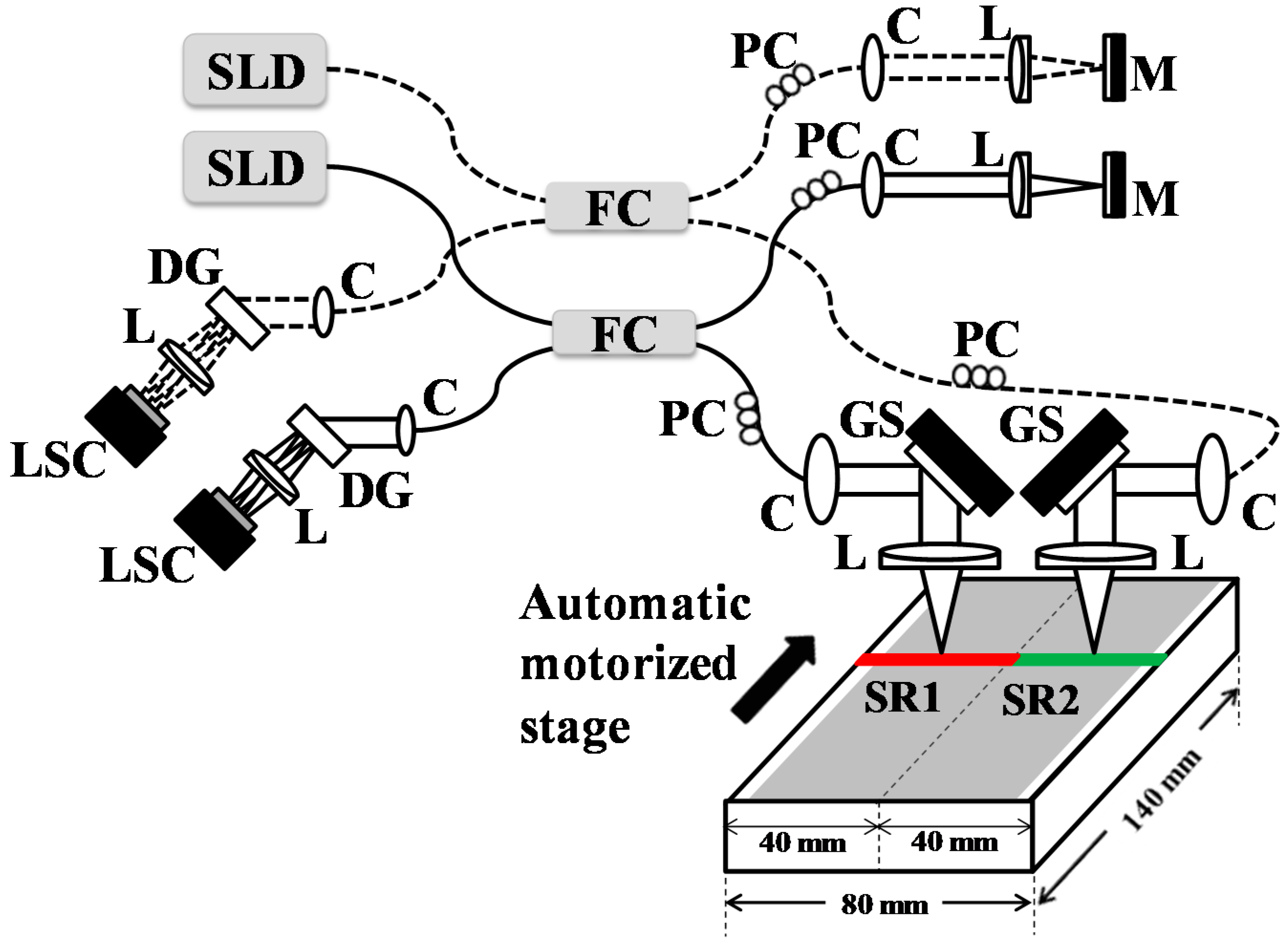
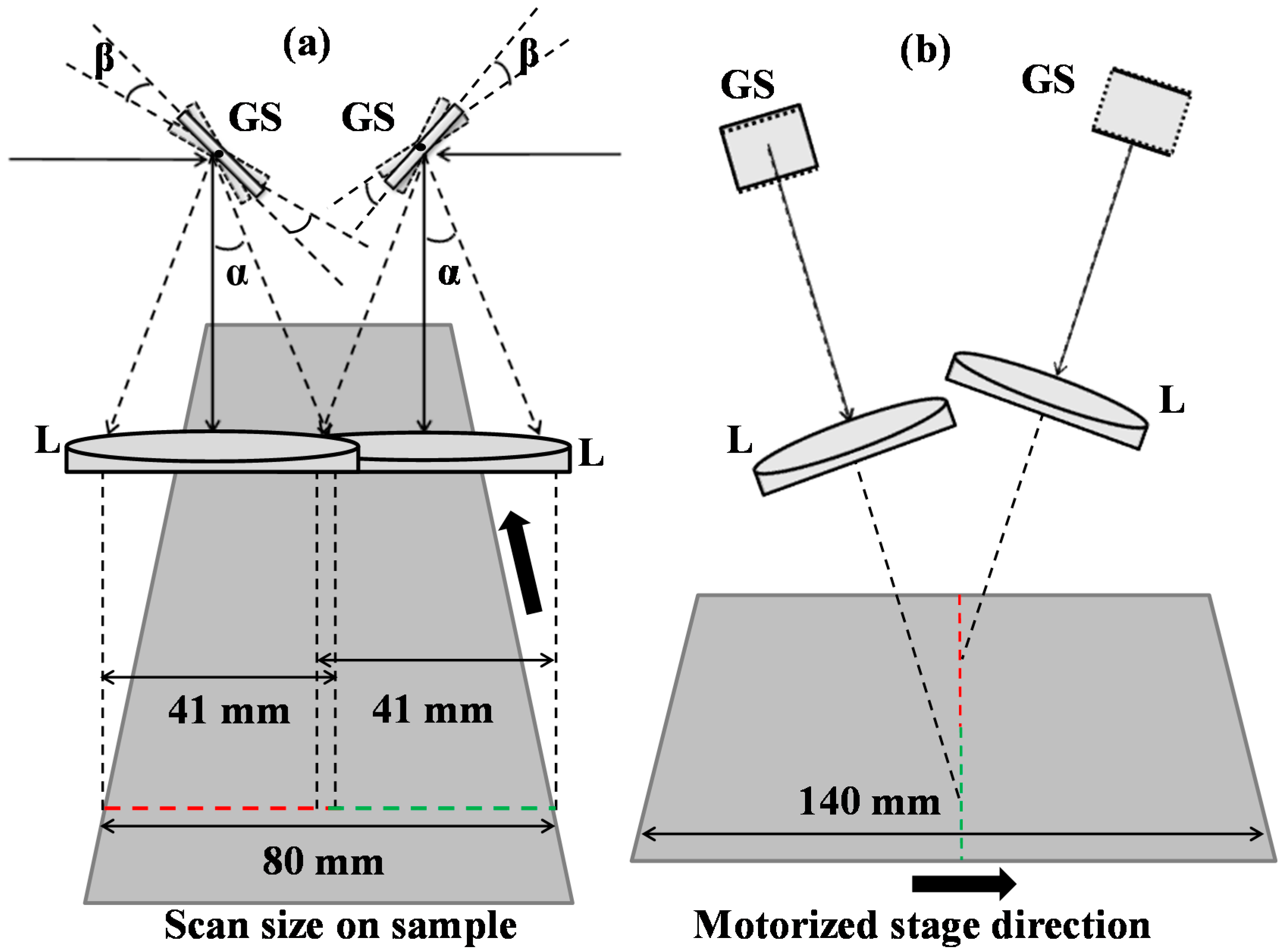
2.1. Hardware Setup
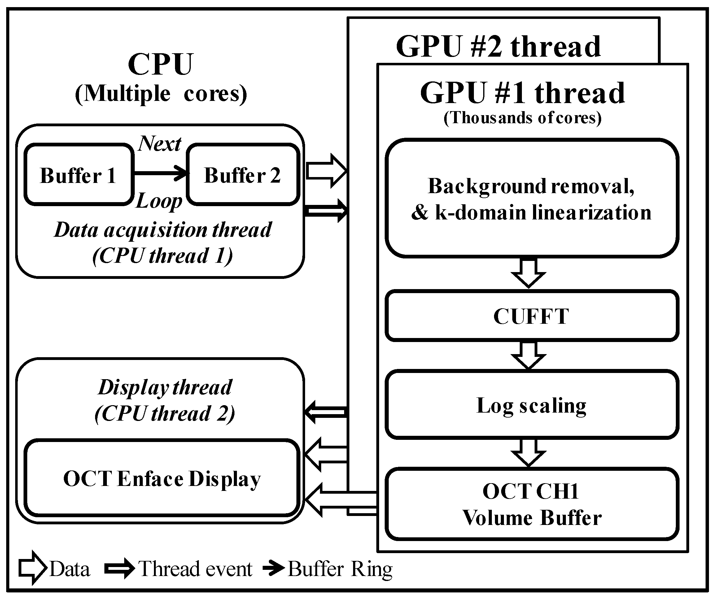
2.2. Software Setup
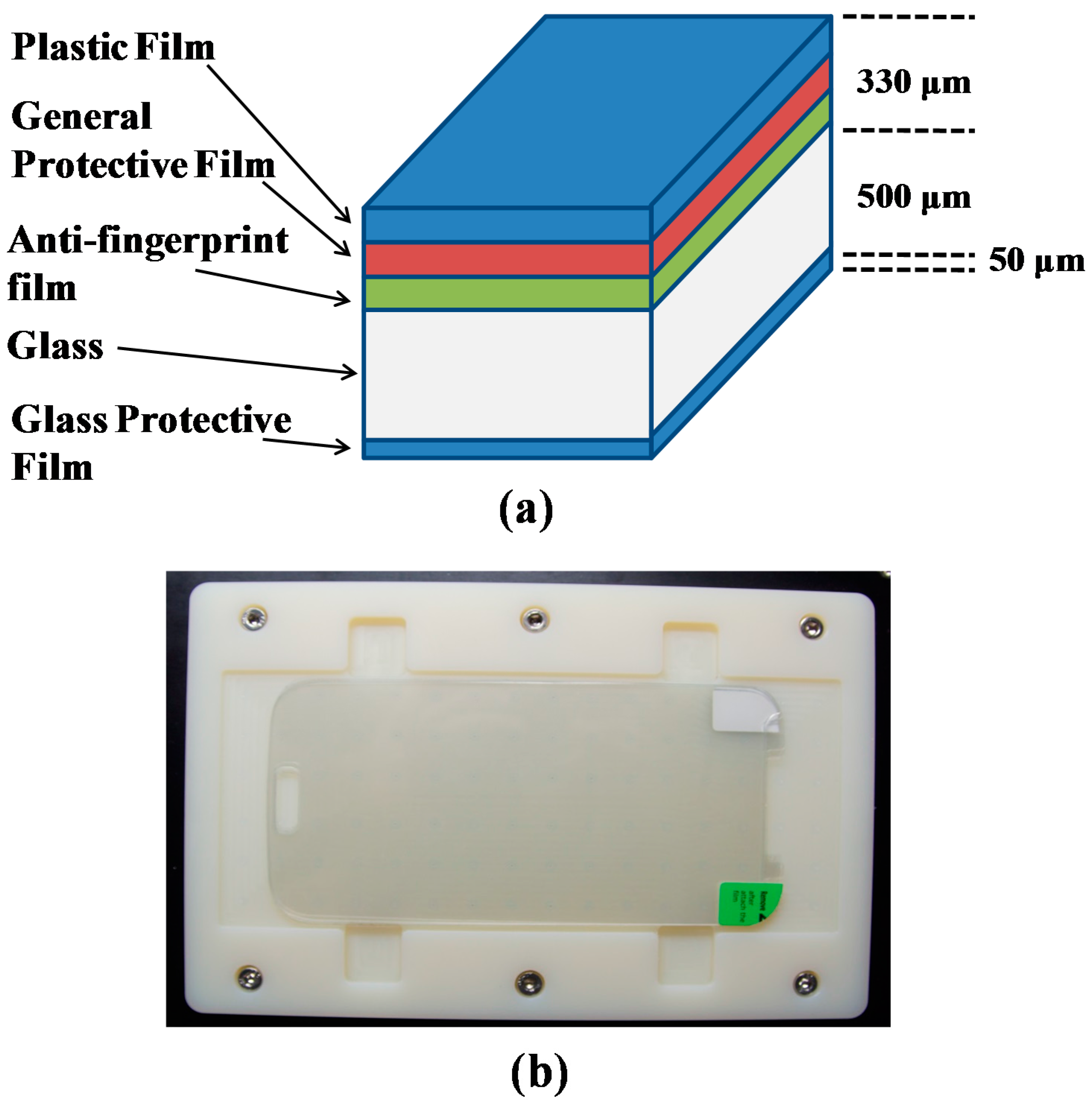
2.3. Materials
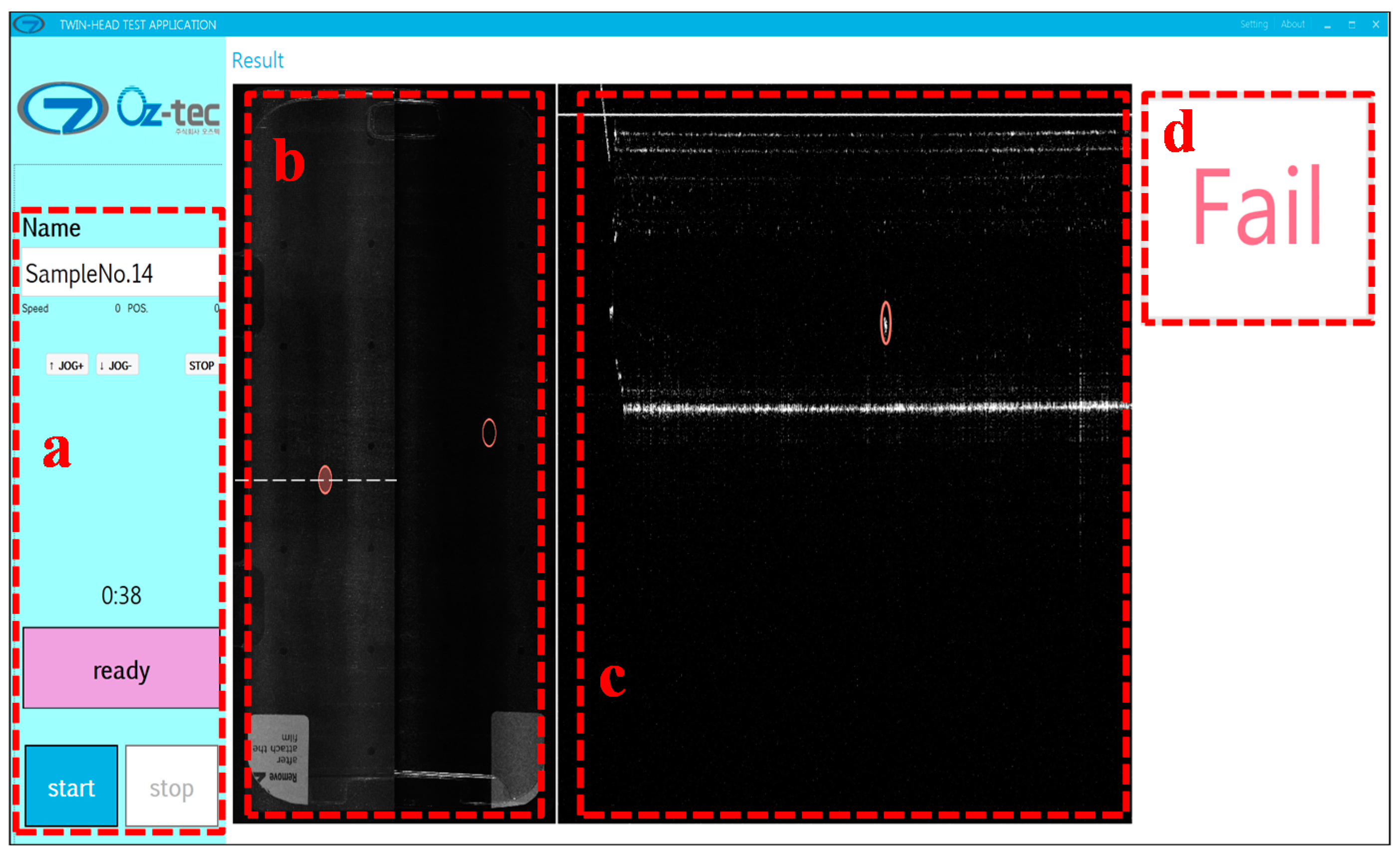
2.4. Graphical User Interface
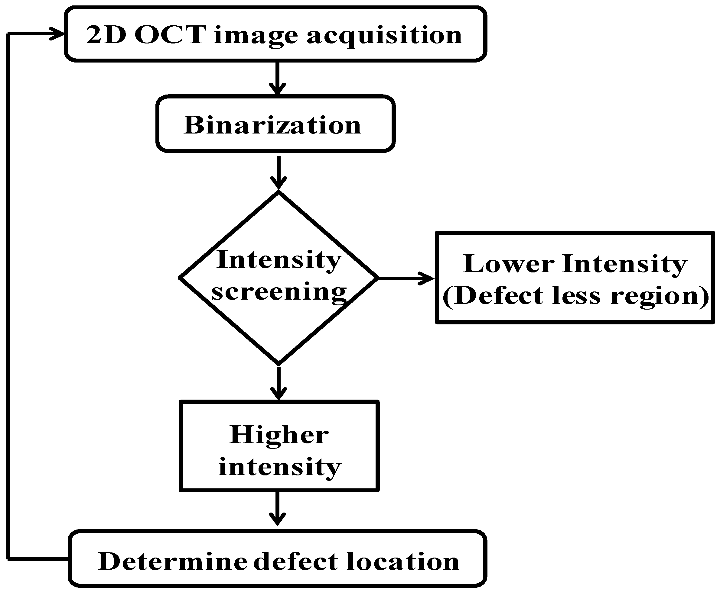
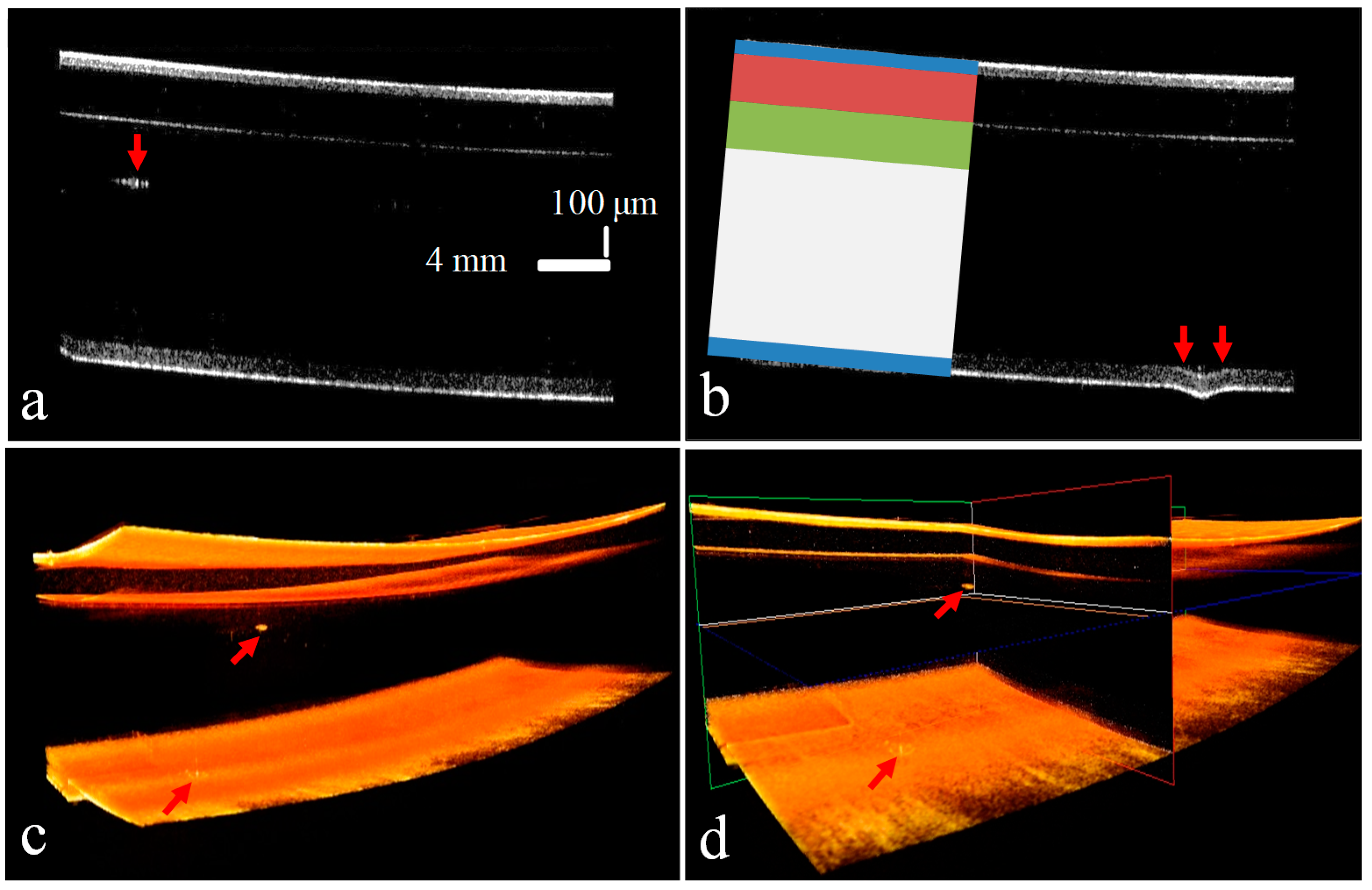
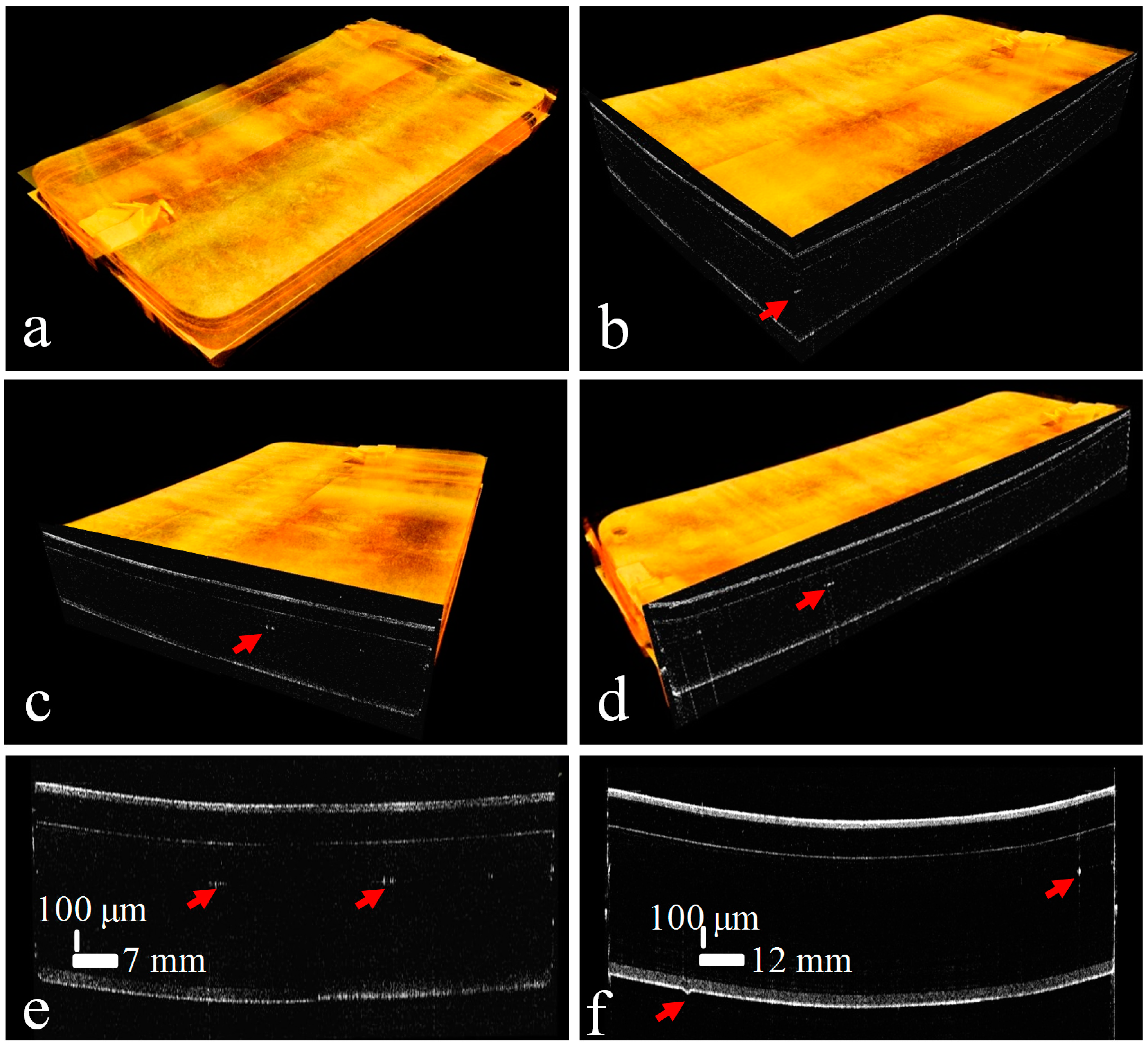
3. Results and Discussion
4. Conclusions
Acknowledgments
Author Contributions
Conflicts of Interest
References
- Rao, A.R. Future directions in industrial machine vision: A case study of semiconductor manufacturing applications. Image Vis. Comput. 1996, 14, 3–19. [Google Scholar] [CrossRef]
- Kim, J.-H.; Ahn, S.; Jeon, J.W.; Byun, J.-E. A high-speed high-resolution vision system for the inspection of TFT LCD. 2001. In Proceedings of the IEEE International Symposium on Industrial Electronics (ISIE 2001), Pusan, Korea, 12–16 June 2001; pp. 101–105.
- Lu, C.-J.; Tsai, D.-M. Automatic defect inspection for lcds using singular value decomposition. Int. J. Adv. Manuf. Technol. 2005, 25, 53–61. [Google Scholar] [CrossRef]
- Wen, Z.; Tao, Y. Building a rule-based machine-vision system for defect inspection on apple sorting and packing lines. Expert Syst. Appl. 1999, 16, 307–313. [Google Scholar] [CrossRef]
- Stojanovic, R.; Mitropulos, P.; Koulamas, C.; Karayiannis, Y.; Koubias, S.; Papadopoulos, G. Real-time vision-based system for textile fabric inspection. Real-Time Imaging 2001, 7, 507–518. [Google Scholar] [CrossRef]
- Baykut, A.; Atalay, A.; Erçil, A.; Güler, M. Real-time defect inspection of textured surfaces. Real-Time Imaging 2000, 6, 17–27. [Google Scholar] [CrossRef]
- Park, N.K.; Yoo, S.I. Evaluation of TFT-LCD defects based on human visual perception. Displays 2009, 30, 1–16. [Google Scholar] [CrossRef]
- Lee, J.Y.; Yoo, S.I. Automatic detection of region-mura defect in TFT-LCD. IEICE Trans. Inf. Syst. 2004, E87-D, 2371–2378. [Google Scholar]
- Gladden, L.F. Process tomography: Principles, techniques and applications. Meas. Sci. Technol. 1997, 8. [Google Scholar] [CrossRef]
- Salvo, L.; Cloetens, P.; Maire, E.; Zabler, S.; Blandin, J.J.; Buffière, J.Y.; Ludwig, W.; Boller, E.; Bellet, D.; Josserond, C. X-ray micro-tomography an attractive characterisation technique in materials science. Nucl. Instrum. Methods Phys. Res. Sect. B Beam Interact. Mater. Atoms. 2003, 200, 273–286. [Google Scholar] [CrossRef]
- Huang, D.; Swanson, E.A.; Lin, C.P.; Schuman, J.S.; Stinson, W.G.; Chang, W.; Hee, M.R.; Flotte, T.; Gregory, K.; Puliafito, C.A.; et al. Optical coherence tomography. Science 1991, 254, 1178–1181. [Google Scholar] [CrossRef] [PubMed]
- Drexler, W.; Morgner, U.; Ghanta, R.K.; Kärtner, F.X.; Schuman, J.S.; Fujimoto, J.G. Ultrahigh-resolution ophthalmic optical coherence tomography. Nat. Med. 2001, 7, 502–507. [Google Scholar] [CrossRef] [PubMed]
- Cui, D.; Liu, X.; Zhang, J.; Yu, X.; Ding, S.; Luo, Y.; Gu, J.; Shum, P.; Liu, L. Dual spectrometer system with spectral compounding for 1-μm optical coherence tomography in vivo. Opt. Lett. 2014, 39, 6727–6730. [Google Scholar] [CrossRef] [PubMed]
- Simavli, H.; Que, C.J.; Akduman, M.; Rizzo, J.L.; Tsikata, E.; de Boer, J.F.; Chen, T.C. Diagnostic capability of peripapillary retinal thickness in glaucoma using 3d volume scans. Am. J. Ophthalmol. 2014, 159, 545–556. [Google Scholar] [CrossRef] [PubMed]
- Braaf, B.; Vermeer, K.A.; de Groot, M.; Vienola, K.V.; de Boer, J.F. Fiber-based polarization-sensitive swept-source oct of the human retina at 1 μm. Investig. Ophtalmol. Vis. Sci. 2014, 55, 1626. [Google Scholar]
- Jung, W.; Kim, J.; Jeon, M.; Chaney, E.J.; Stewart, C.N.; Boppart, S.A. Handheld optical coherence tomography scanner for primary care diagnostics. IEEE Trans. Biomed. Eng. 2011, 58, 741–744. [Google Scholar] [CrossRef] [PubMed]
- Lee, C.; Kim, K.; Han, S.; Kim, S.; Lee, J.H.; Kim, H.K.; Kim, C.; Jung, W.; Kim, J. Stimulated penetrating keratoplasty using real-time virtual intraoperative surgical optical coherence tomography. J. Biomed. Opt. 2014, 19, 030502. [Google Scholar] [CrossRef] [PubMed]
- Gambichler, T.; Moussa, G.; Sand, M.; Sand, D.; Altmeyer, P.; Hoffmann, K. Applications of optical coherence tomography in dermatology. J. Dermatol. Sci. 2005, 40, 85–94. [Google Scholar] [CrossRef] [PubMed]
- Lee, R.C.; Kang, H.; Darling, C.L.; Fried, D. Automated assessment of the remineralization of artificial enamel lesions with polarization-sensitive optical coherence tomography. Biomed. Opt. Express 2014, 5, 2950–2962. [Google Scholar] [CrossRef] [PubMed]
- Cho, N.H.; Jang, J.H.; Jung, W.; Kim, J. In vivo imaging of middle-ear and inner-ear microstructures of a mouse guided by SD-OCT combined with a surgical microscope. Opt. Express 2014, 22, 8985–8995. [Google Scholar] [CrossRef] [PubMed]
- Cho, N.H.; Lee, J.W.; Cho, J.-H.; Kim, J.; Jang, J.H.; Jung, W. Evaluation of the usefulness of three-dimensional optical coherence tomography in a guinea pig model of endolymphatic hydrops induced by surgical obliteration of the endolymphatic duct. J. Biomed. Opt. 2015, 20, 036009. [Google Scholar] [CrossRef] [PubMed]
- Cho, N.H.; Lee, S.H.; Jung, W.; Jang, J.H.; Kim, J. Optical coherence tomography for the diagnosis and evaluation of human otitis media. J. Korean Med. Sci. 2015, 30, 328–335. [Google Scholar] [CrossRef] [PubMed]
- Kut, C.; Chaichana, K.L.; Xi, J.; Raza, S.M.; Ye, X.; McVeigh, E.R.; Rodriguez, F.J.; Quiñones-Hinojosa, A.; Li, X. Detection of human brain cancer infiltration ex vivo and in vivo using quantitative optical coherence tomography. Sci. Transl. Med. 2015, 7. [Google Scholar] [CrossRef] [PubMed]
- Lee, C.; Lee, S.-Y.; Kim, J.-Y.; Jung, H.-Y.; Kim, J. Optical sensing method for screening disease in melon seeds by using optical coherence tomography. Sensors 2011, 11, 9467–9477. [Google Scholar] [CrossRef] [PubMed]
- Ravichandran, N.K.; Wijesinghe, R.E.; Shirazi, M.F.; Park, K.; Lee, S.-Y.; Jung, H.-Y.; Jeon, M.; Kim, J. In vivo monitoring on growth and spread of gray leaf spot disease in capsicum annuum leaf using spectral domain optical coherence tomography. J. Spectrosc. 2016, 2016, 1093734. [Google Scholar] [CrossRef]
- Lee, S.-Y.; Lee, C.; Kim, J.; Jung, H.-Y. Application of optical coherence tomography to detect cucumber green mottle mosaic virus (CGMMV) infected cucumber seed. Hortic. Environ. Biotechnol. 2012, 53, 428–433. [Google Scholar] [CrossRef]
- Fujimoto, J.G. Optical coherence tomography for ultrahigh resolution in vivo imaging. Nat. Biotechnol. 2003, 21, 1361–1367. [Google Scholar] [CrossRef] [PubMed]
- Shirazi, M.F.; Cho, N.H.; Jung, W.; Kim, J. Lateral resolution enhancement using programmable phase modulator in optical coherence tomography. Bio-Med. Mater. Eng. 2015, 26, S1465–S1471. [Google Scholar] [CrossRef] [PubMed]
- Lee, S.W.; Jeong, H.W.; Kim, B.M.; Ahn, Y.C.; Jung, W.; Chen, Z. Optimization for axial resolution, depth range, and sensitivity of spectral domain optical coherence tomography at 1.3 microm. J. Korean Phys. Soc. 2009, 55, 2354–2360. [Google Scholar] [PubMed]
- Cho, N.H.; Park, K.; Kim, J.-Y.; Jung, Y.; Kim, J. Quantitative assessment of touch-screen panel by nondestructive inspection with three-dimensional real-time display optical coherence tomography. Opt. Lasers Eng. 2015, 68, 50–57. [Google Scholar] [CrossRef]
- Ju, M.J.; Lee, S.J.; Kim, Y.; Shin, J.G.; Kim, H.Y.; Lim, Y.; Yasuno, Y.; Lee, B.H. Multimodal analysis of pearls and pearl treatments by using optical coherence tomography and fluorescence spectroscopy. Opt. Express 2011, 19, 6420–6432. [Google Scholar] [CrossRef] [PubMed]
- Choi, W.-J.; Min, G.-H.; Lee, B.-H.; Eom, J.-H.; Kim, J.-W. Counterfeit detection using characterization of safety feature on banknote with full-field optical coherence tomography. J. Opt. Soc. Korea 2010, 14, 316–320. [Google Scholar] [CrossRef]
- Kim, S.-H.; Kim, J.-H.; Kang, S.-W. Nondestructive defect inspection for LCDs using optical coherence tomography. Displays 2011, 32, 325–329. [Google Scholar] [CrossRef]
- Stifter, D. Beyond biomedicine: A review of alternative applications and developments for optical coherence tomography. Appl. Phys. B 2007, 88, 337–357. [Google Scholar] [CrossRef]
- Chen, Z.; Zhao, C.; Shen, Y.; Li, P.; Wang, X.; Ding, Z. Ultrawide-field parallel spectral domain optical coherence tomography for nondestructive inspection of glass. Opt. Commun. 2015, 341, 122–130. [Google Scholar] [CrossRef]
- Bashkansky, M.; Duncan, M.; Kahn, M.; Lewis, D.; Reintjes, J. Subsurface defect detection in ceramics by high-speed high-resolution optical coherent tomography. Opt. Lett. 1997, 22, 61–63. [Google Scholar] [CrossRef] [PubMed]
- Duncan, M.D.; Bashkansky, M.; Reintjes, J. Subsurface defect detection in materials using optical coherence tomography. Opt. Express 1998, 2, 540–545. [Google Scholar] [CrossRef] [PubMed]
- Cho, N.H.; Jung, U.; Kim, S.; Kim, J. Non-destructive inspection methods for leds using real-time displaying optical coherence tomography. Sensors 2012, 12, 10395–10406. [Google Scholar] [CrossRef] [PubMed]
- Suehira, N.; Ooto, S.; Hangai, M.; Matsumoto, K.; Tomatsu, N.; Yuasa, T.; Yamada, K.; Yoshimura, N. Three-beam spectral-domain optical coherence tomography for retinal imaging. J. Biomed. Opt. 2012, 17, 106001. [Google Scholar] [CrossRef] [PubMed]
- Jeon, M.; Kim, J.; Jung, U.; Lee, C.; Jung, W.; Boppart, S.A. Full-range k-domain linearization in spectral-domain optical coherence tomography. Appl. Opt. 2011, 50, 1158–1163. [Google Scholar] [CrossRef] [PubMed]
- Jung, U.-S.; Cho, N.-H.; Kim, S.-H.; Jeong, H.-S.; Kim, J.-H.; Ahn, Y.-C. Simple spectral calibration method and its application using an index array for swept source optical coherence tomography. J. Opt. Soc. Korea 2011, 15, 386–393. [Google Scholar] [CrossRef]
- Bradu, A.; Maria, M.; Podoleanu, A.G. Demonstration of tolerance to dispersion of master/slave interferometry. Opt. Express 2015, 23, 14148–14161. [Google Scholar] [CrossRef] [PubMed]
- Jeong, H.; Cho, N.H.; Jung, U.; Lee, C.; Kim, J.-Y.; Kim, J. Ultra-fast displaying spectral domain optical doppler tomography system using a graphics processing unit. Sensors 2012, 12, 6920–6929. [Google Scholar] [CrossRef] [PubMed]


© 2016 by the authors; licensee MDPI, Basel, Switzerland. This article is an open access article distributed under the terms and conditions of the Creative Commons Attribution (CC-BY) license (http://creativecommons.org/licenses/by/4.0/).
Share and Cite
Shirazi, M.F.; Park, K.; Wijesinghe, R.E.; Jeong, H.; Han, S.; Kim, P.; Jeon, M.; Kim, J. Fast Industrial Inspection of Optical Thin Film Using Optical Coherence Tomography. Sensors 2016, 16, 1598. https://doi.org/10.3390/s16101598
Shirazi MF, Park K, Wijesinghe RE, Jeong H, Han S, Kim P, Jeon M, Kim J. Fast Industrial Inspection of Optical Thin Film Using Optical Coherence Tomography. Sensors. 2016; 16(10):1598. https://doi.org/10.3390/s16101598
Chicago/Turabian StyleShirazi, Muhammad Faizan, Kibeom Park, Ruchire Eranga Wijesinghe, Hyosang Jeong, Sangyeob Han, Pilun Kim, Mansik Jeon, and Jeehyun Kim. 2016. "Fast Industrial Inspection of Optical Thin Film Using Optical Coherence Tomography" Sensors 16, no. 10: 1598. https://doi.org/10.3390/s16101598