
Influences of an Aluminum Covering Layer on the Performance of Cross-Like Hall Devices

Abstract
:1. Introduction
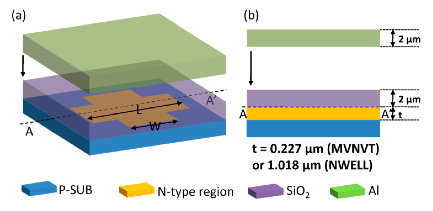
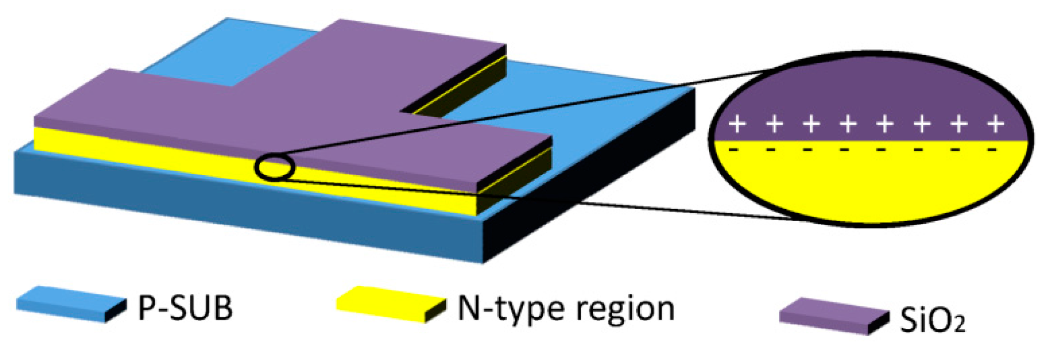
2. Design and Experiment

3. Results and Discussion
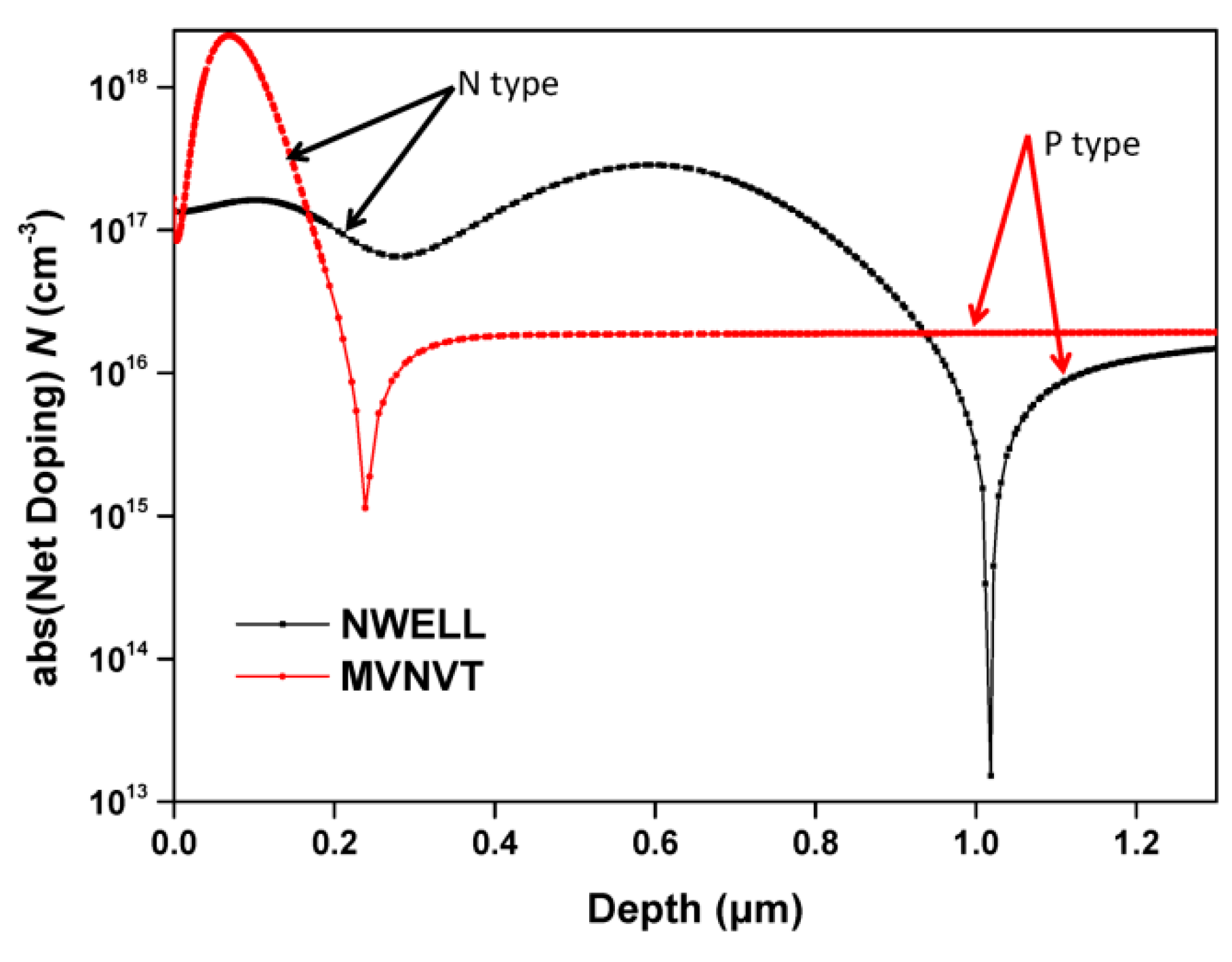
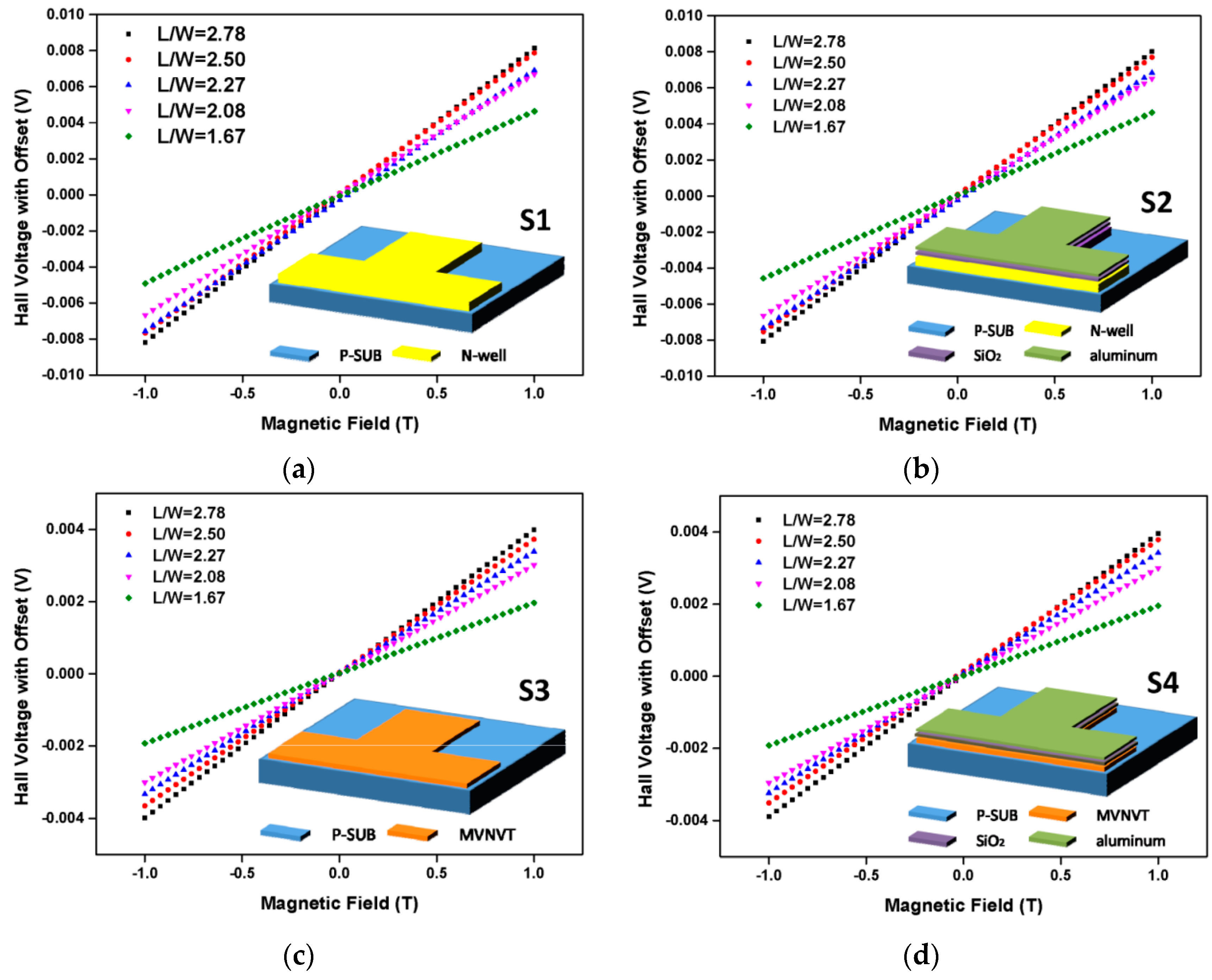
3.1. Hall Device

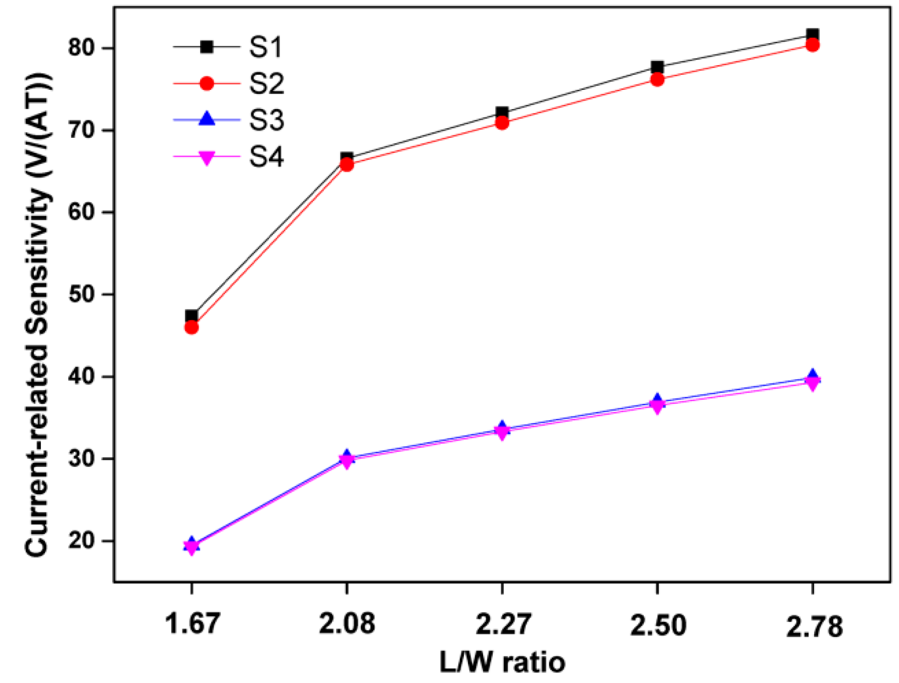
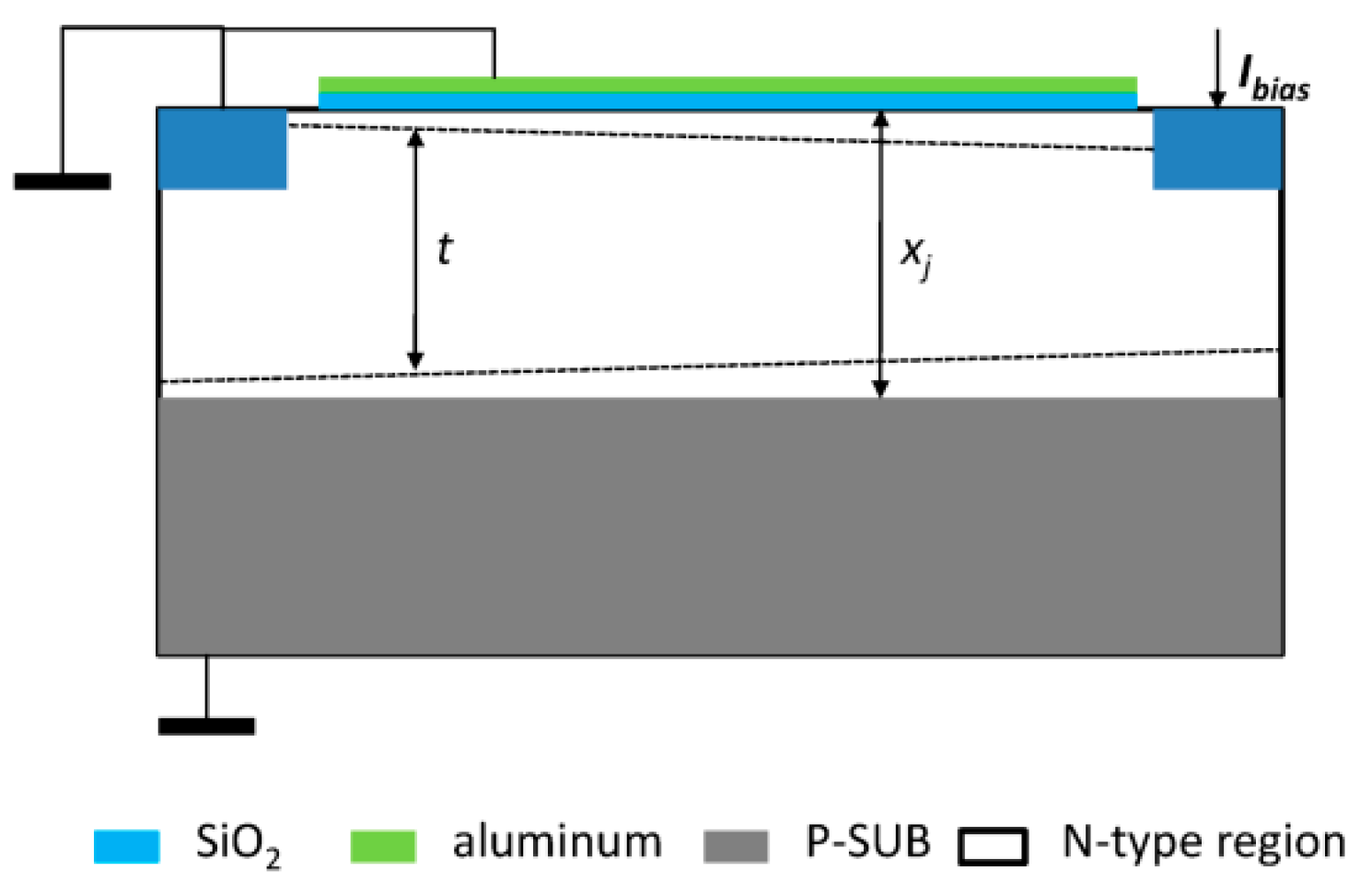
3.2. Current-Related Sensitivity


| Bp (T) | D (m) | P (Ω·m) | D (kg/m3) |
|---|---|---|---|
| 0~1 | 2 × 10⁻⁶ | 2.83 × 10⁻⁸ | 2.7 × 10³ |
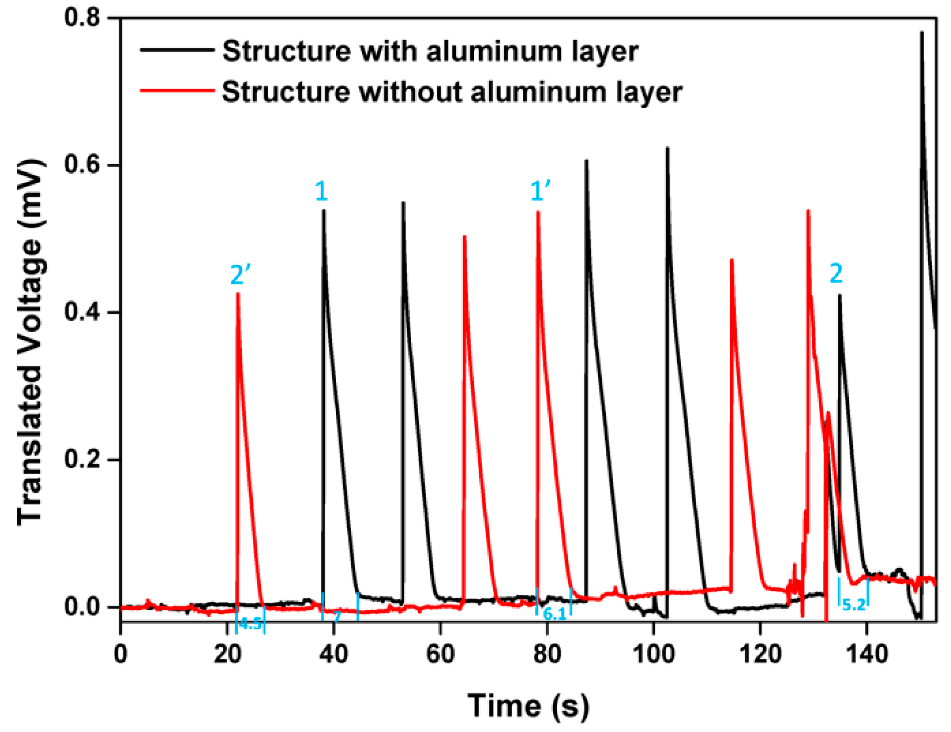
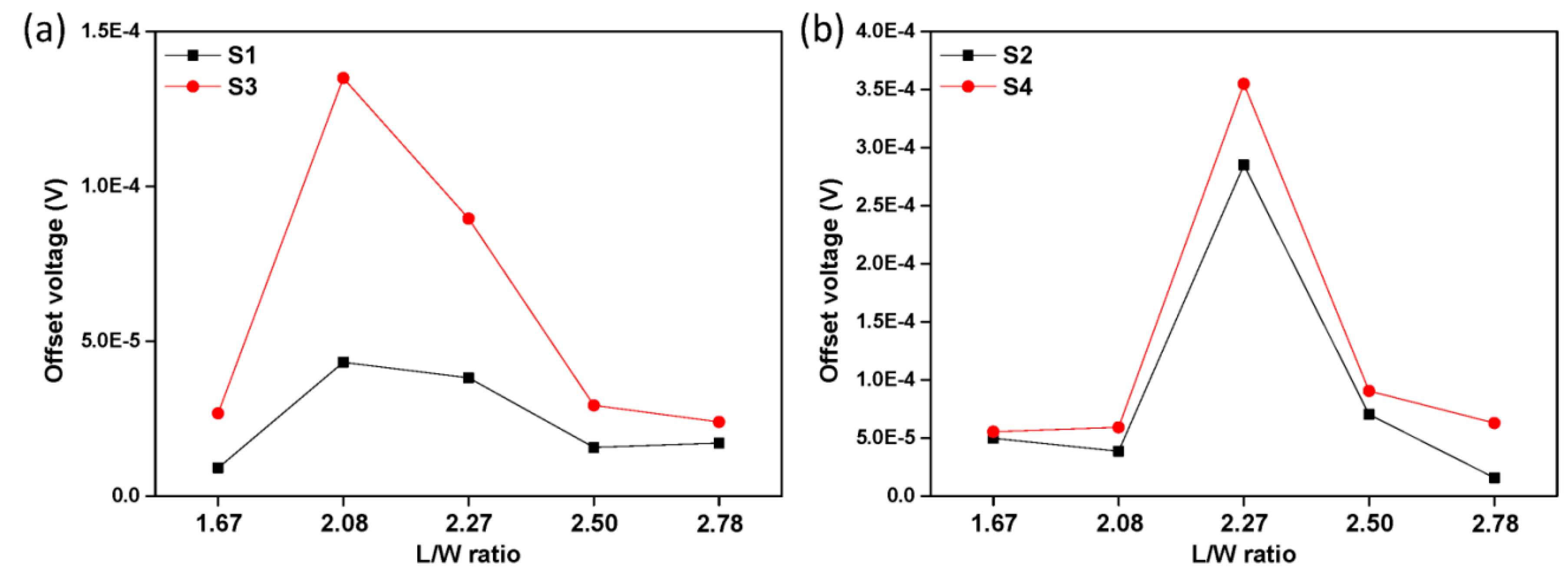
3.3. Offset Voltage

4. Conclusions
Acknowledgments
Author Contributions
Conflicts of Interest
References
- Ramsden, E. Hall-Effect Sensors: Theory and Application; Elsevier: Philadelphia, PA, USA, 2011. [Google Scholar]
- Popovic, R.S. Hall Effect Devices; CRC Press: Boca Raton, FL, USA, 2003. [Google Scholar]
- Boero, G.; Demierre, M.; Popovic, R. Micro-Hall devices: Performance, technologies and applications. Sens. Actuators A Phys. 2003, 106, 314–320. [Google Scholar] [CrossRef]
- Paun, M.-A.; Sallese, J.-M.; Kayal, M. Comparative study on the performance of five different Hall effect devices. Sensors 2013, 13, 2093–2112. [Google Scholar] [CrossRef] [PubMed]
- Paun, M.-A.; Sallese, J.-M.; Kayal, M. Offset and drift analysis of the Hall Effect sensors. The geometrical parameters influence. Dig. J. Nanomater. Biostruct 2012, 7, 883–891. [Google Scholar]
- Paun, M.-A.; Sallese, J.-M.; Kayal, M. Geometrical Parameters Influence on the Hall Effect Sensors Offset and Drift. In Proceedings of the 7th Conference on Ph.D. Research in Microelectronics and Electronics (PRIME), Trento, Italy, 3–7 July 2011; pp. 145–148.
- Paun, M.-A.; Sallese, J.-M.; Kayal, M. Hall effect sensors design, integration and behavior analysis. J. Sens. Actuator Netw. 2013, 2, 85–97. [Google Scholar] [CrossRef]
- Paun, M.-A.; Sallese, J.-M.; Kayal, M. A specific parameters analysis of CMOS Hall effect sensors with various geometries. In Proceedings of the 19th International Conference Mixed Design of Integrated Circuits and Systems (MIXDES), Warsaw, Poland, 24–26 May 2012; pp. 335–339.
- Paun, M.-A.; Sallese, J.-M.; Kayal, M. Hall effect sensors performance investigation using three-dimensional simulations. In Proceedings of the 18th International Conference on Mixed Design of Integrated Circuits and Systems (MIXDES), Gliwice, Poland, 16–18 June 2011; pp. 450–455.
- Versnel, W. Analysis of symmetrical Hall plates with finite contacts. J. Appl. Phys. 1981, 52, 4659–4666. [Google Scholar] [CrossRef]
- Versnel, W. The geometrical correction factor for a rectangular Hall plate. J. Appl. Phys. 1982, 53, 4980–4986. [Google Scholar] [CrossRef]
- Heidari, H.; Gatti, U.; Bonizzoni, E.; Maloberti, F. Low-noise low-Offset current-mode Hall sensors. In Proceedings of the 9th Conference on Ph. D. Research in Microelectronics and Electronics (PRIME), Villach, Austria, 24–27 June 2013; pp. 325–328.
- Heidari, H.; Bonizzoni, E.; Gatti, U.; Maloberti, F. A CMOS Current-Mode Magnetic Hall Sensor with Integrated Front-End. IEEE Trans. Circuits Syst. I Regul. Pap. 2015, 62, 1270–1278. [Google Scholar] [CrossRef]
- Heidari, H.; Bonizzoni, E.; Gatti, U.; Maloberti, F. A 0.18-μm CMOS Current-Mode Hall Magnetic Sensor with Very Low Bias Current and High Sensitive Front-End. In Proceedings of the IEEE SENSORS, Valencia, Spain, 2–5 November 2014; pp. 1467–1470.
- Heidari, H.; Bonizzoni, E.; Gatti, U.; Maloberti, F.A. Current-Mode CMOS integrated microsystem for current spinning magnetic hall sensors. In Proceedings of the IEEE International Symposium on Circuits and Systems (ISCAS), Melbourne, Australia, 1–5 June 2014; pp. 678–681.
- Paun, M.-A. Three-dimensional simulations in optimal performance trial between two types of Hall sensors fabrication technologies. J. Magn. Magn. Mater. 2015, 391, 122–128. [Google Scholar] [CrossRef]
- Huang, H.; Wang, D.; Xu, Y. A Monolithic CMOS Magnetic Hall Sensor with High Sensitivity and Linearity Characteristics. Sensors 2015, 15, 27359–27373. [Google Scholar] [CrossRef] [PubMed]
- Schweda, J.; Riedling, K. A nonlinear simulation model of integrated Hall devices in CMOS silicon technology. In Proceedings of the IEEE International Workshop on Behavioral Modeling and Simulation, Santa Rosa, CA, USA, 6–8 October 2002; pp. 14–20.
- Popović, R. Hall-effect devices. Sens. Actuators 1989, 17, 39–53. [Google Scholar] [CrossRef]
- Lyu, F.; Zhang, Z.; Toh, E.-H.; Liu, X.; Ding, Y.; Pan, Y.; Li, C.; Li, L.; Sha, J.; Pan, H. Performance Comparison of Cross-Like Hall Plates with Different Covering Layers. Sensors 2014, 15, 672–686. [Google Scholar] [CrossRef] [PubMed]
- Xu, Y.; Pan, H.-B. An improved equivalent simulation model for CMOS integrated Hall plates. Sensors 2011, 11, 6284–6296. [Google Scholar] [CrossRef] [PubMed]
- Miessler, G. DA Tarr Inorganic Chemistry; Prentice Hall: Upper Saddle River, NJ, USA, 2013. [Google Scholar]
- Chakravarty, A.S. Introduction to the Magnetic Properties of Solids; John Wiley & Sons: Hoboken, NJ, USA, 1981. [Google Scholar]
- Anderson, B.; Anderson, R. Fundamentals of Semiconductor Devices; McGraw-Hill: New York, NY, USA, 2005. [Google Scholar]
- Fiorillo, F. Measurement and Characterization of Magnetic Materials; Elsevier: Amsterdam, Holland, 2004. [Google Scholar]
- Bellekom, S. CMOS versus bipolar Hall plates regarding offset correction. Sens. Actuators A Phys. 1999, 76, 178–182. [Google Scholar] [CrossRef]
© 2016 by the authors; licensee MDPI, Basel, Switzerland. This article is an open access article distributed under the terms and conditions of the Creative Commons by Attribution (CC-BY) license (http://creativecommons.org/licenses/by/4.0/).
Share and Cite
Lyu, F.; Liu, X.; Ding, Y.; Toh, E.-H.; Zhang, Z.; Pan, Y.; Wang, Z.; Li, C.; Li, L.; Sha, J.; et al. Influences of an Aluminum Covering Layer on the Performance of Cross-Like Hall Devices. Sensors 2016, 16, 106. https://doi.org/10.3390/s16010106
Lyu F, Liu X, Ding Y, Toh E-H, Zhang Z, Pan Y, Wang Z, Li C, Li L, Sha J, et al. Influences of an Aluminum Covering Layer on the Performance of Cross-Like Hall Devices. Sensors. 2016; 16(1):106. https://doi.org/10.3390/s16010106
Chicago/Turabian StyleLyu, Fei, Xinfu Liu, Yinjie Ding, Eng-Huat Toh, Zhenyan Zhang, Yifan Pan, Zhen Wang, Chengjie Li, Li Li, Jin Sha, and et al. 2016. "Influences of an Aluminum Covering Layer on the Performance of Cross-Like Hall Devices" Sensors 16, no. 1: 106. https://doi.org/10.3390/s16010106