
Low-Actuation Voltage MEMS Digital-to-Analog Converter with Parylene Spring Structures

Abstract
:1. Introduction
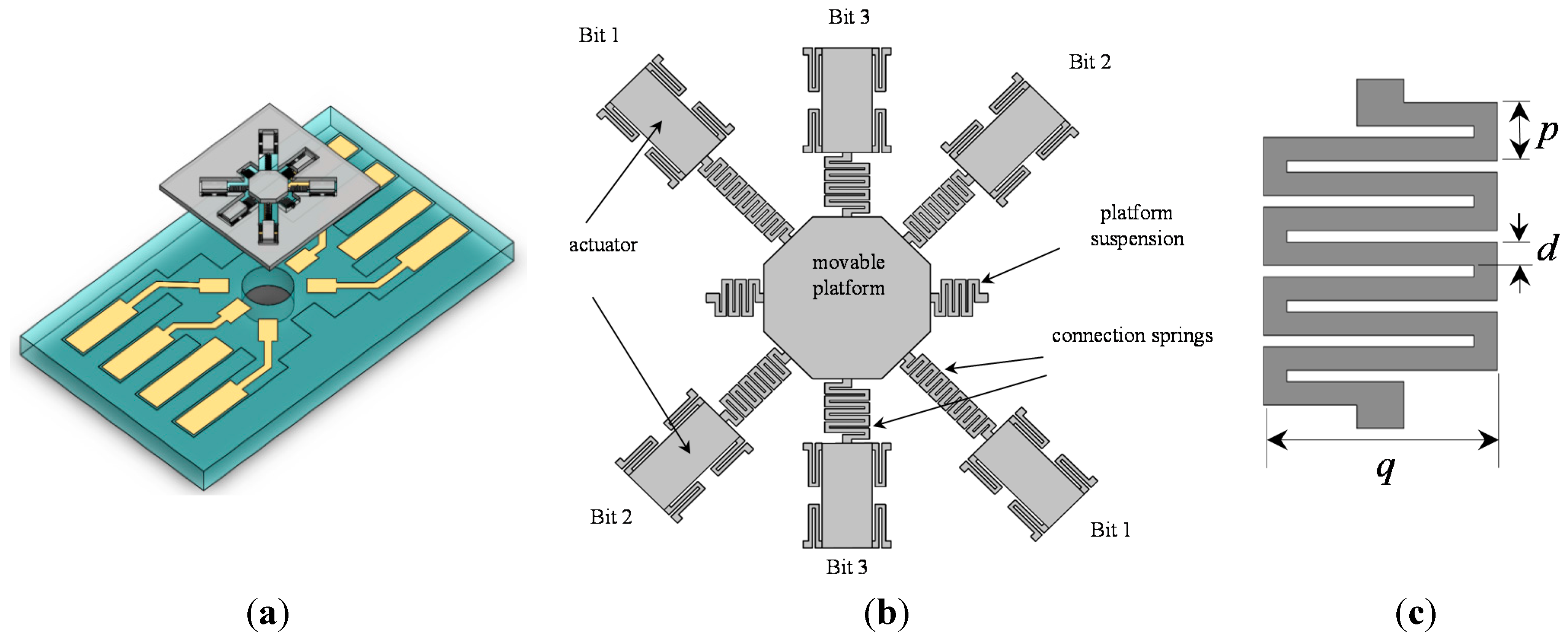
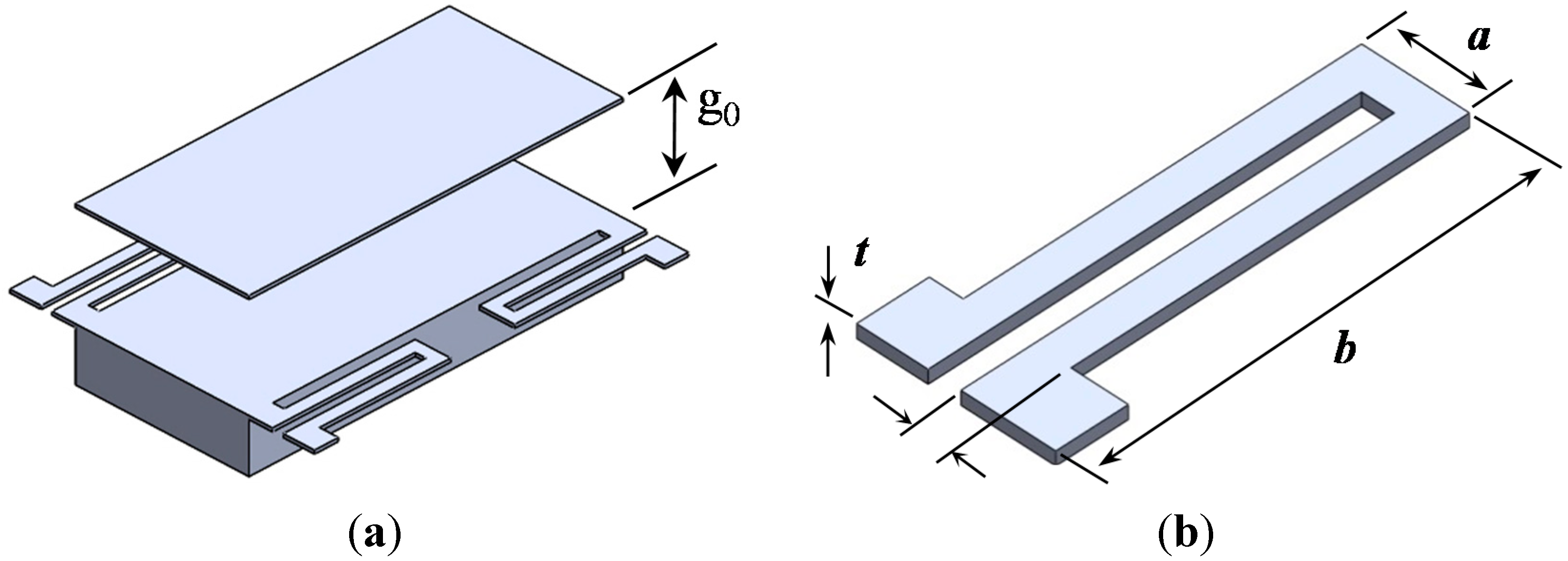
2. M-DAC Design

| Description | Parameters | Definitions/Values |
|---|---|---|
| Length of the spring in x-axis | (μm) | 50 |
| Length of the spring in y-axis | (μm) | 250 |
| Width of the spring | (μm) | 20 |
| Thickness of the spring | (μm) | 10 |
| Plate area | (μm2) | 350,000 |
| Moment of inertia (x-axis) | (μm4) | |
| Torsion constant | (μm4) | [15] |
| Material | Silicon [16] | Parylene-C [17] |
|---|---|---|
| Young’s modulus () | 130.919 GPa | 4 GPa |
| Shear modulus () | 79.92 GPa | 1.67 GPa |
| Material | Silicon | Parylene-C | ||||
|---|---|---|---|---|---|---|
| (N/m) | 226.5810 | 6.0986 | ||||
| (μm) | 2 | 3 | 4 | 2 | 3 | 4 |
| (V) | 13.165 | 24.185 | 37.235 | 2.159 | 3.967 | 6.108 |
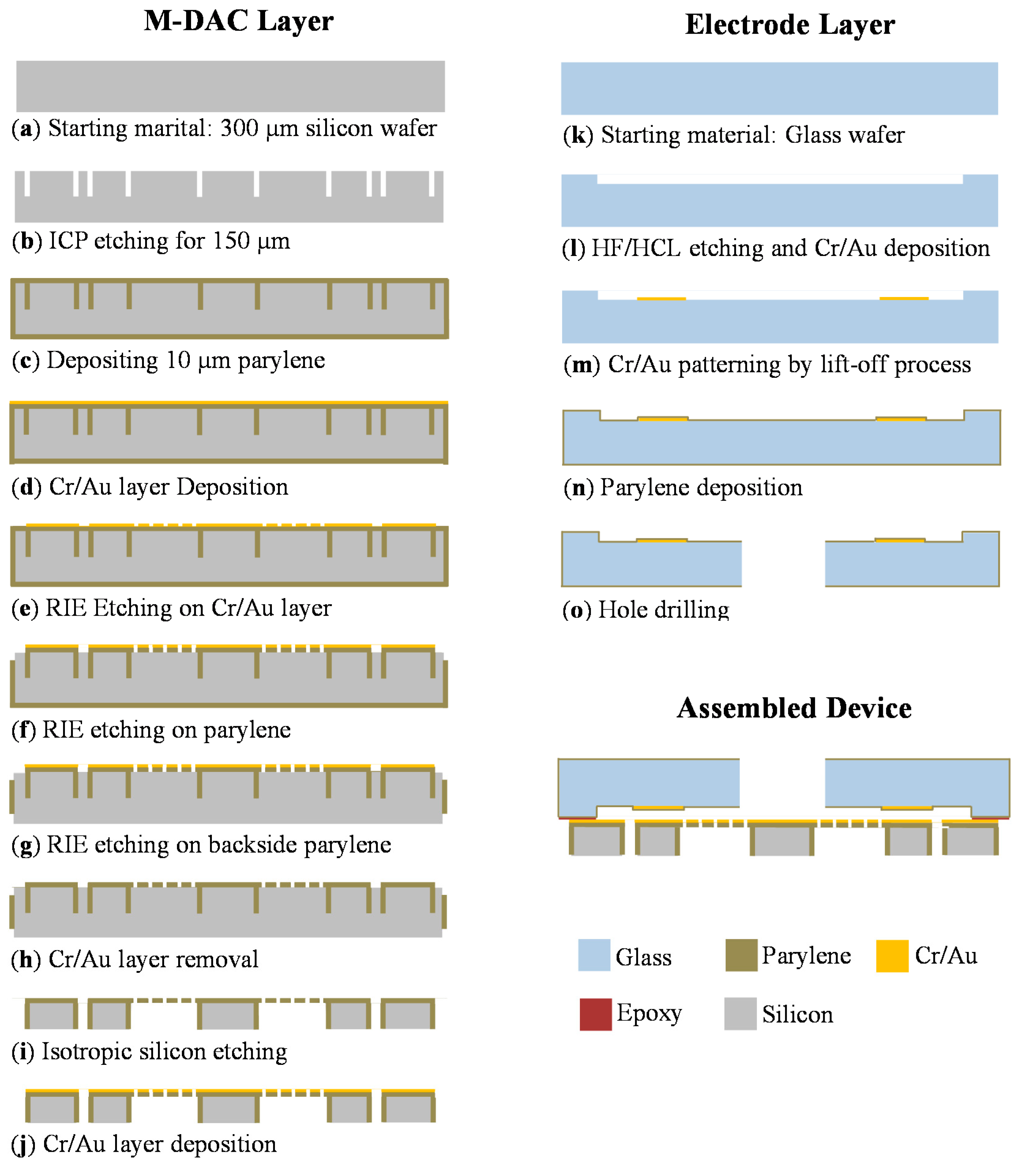
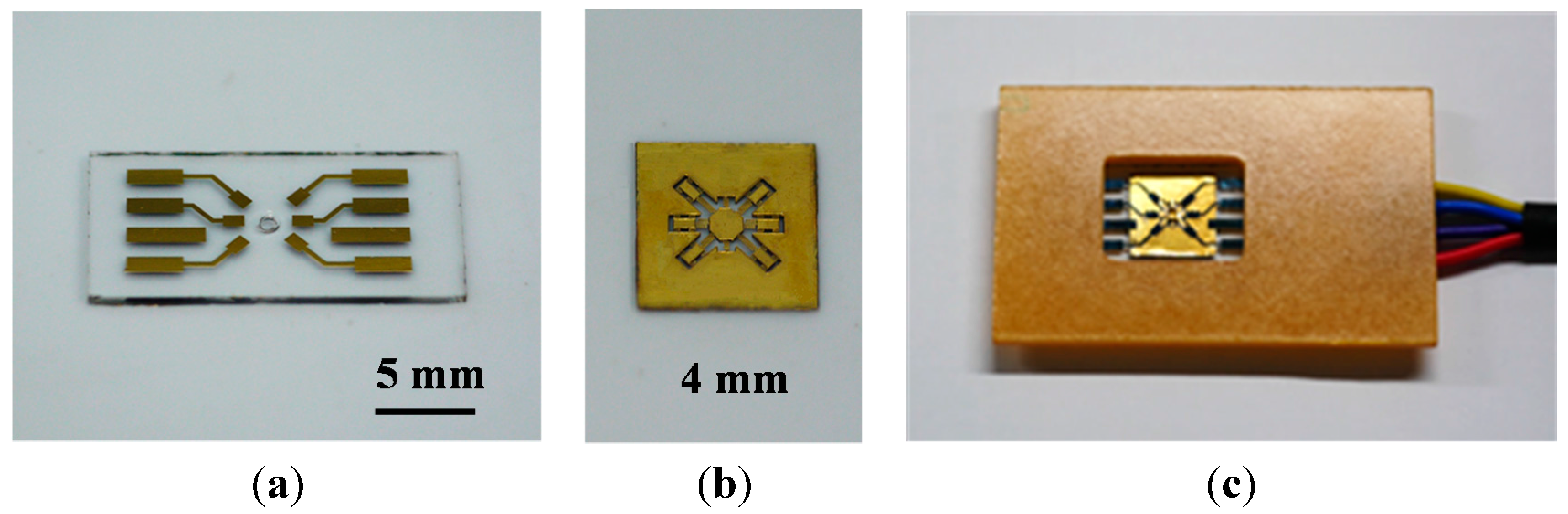
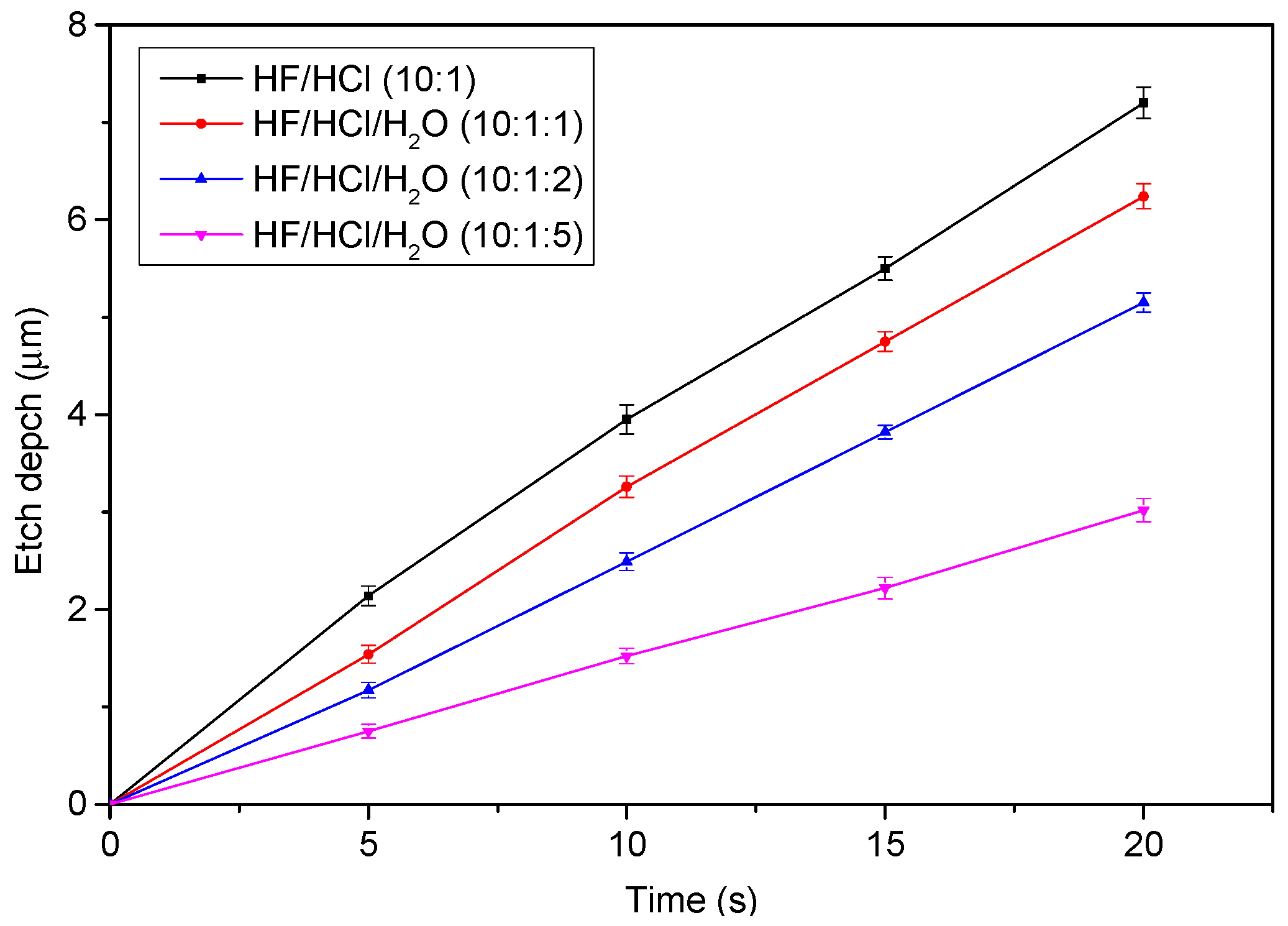
3. Fabrication
3.1. Platform Layer
3.2. Electrode Layer and Device Assembly


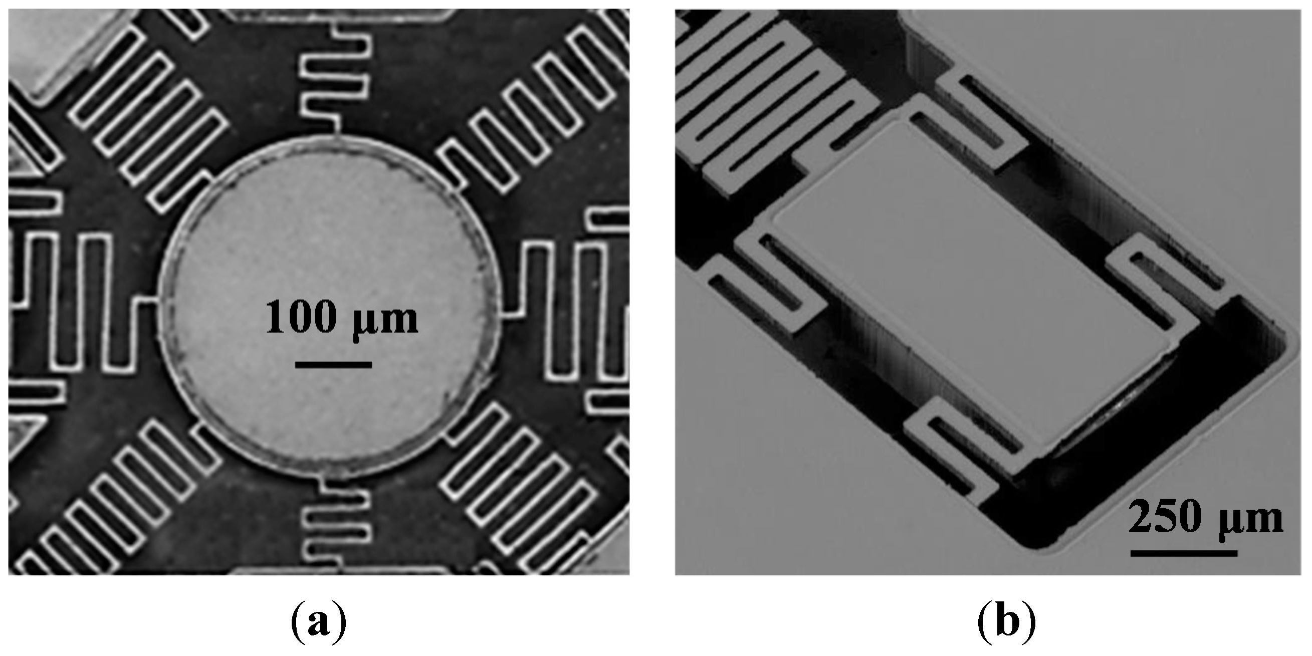
4. Measurement and Discussion
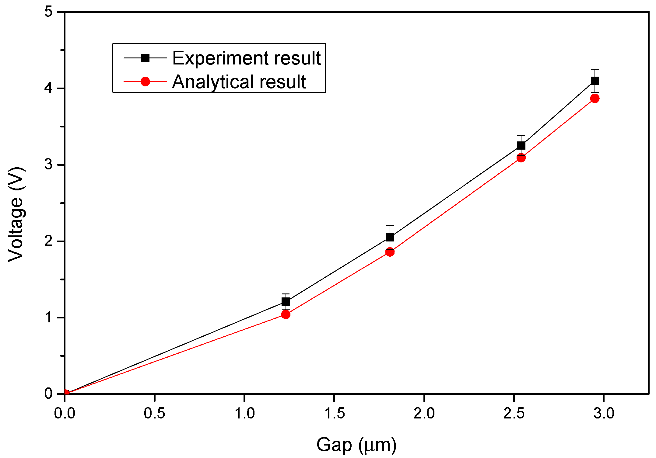
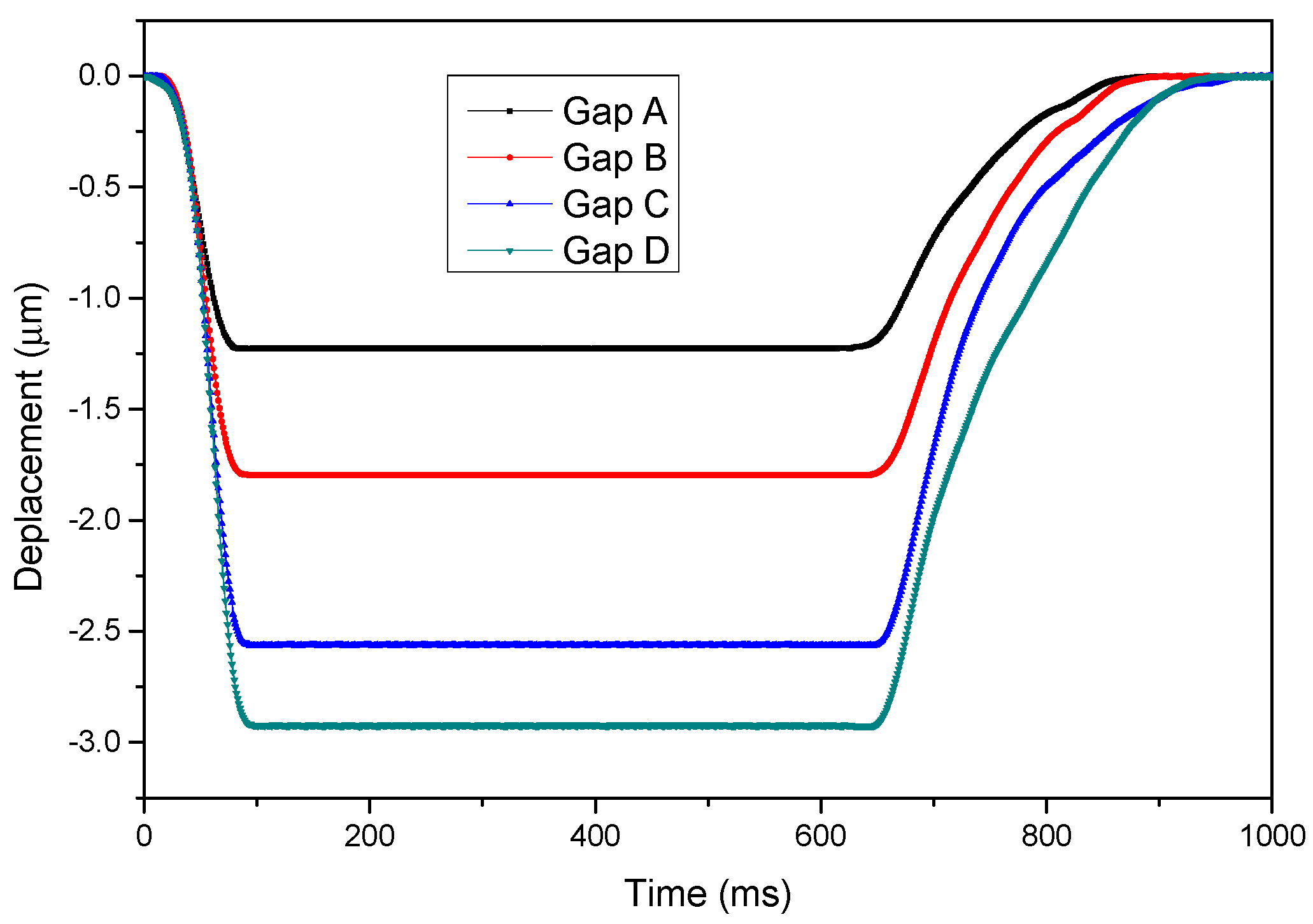
4.1. Electrostatic Actuators


| Mode No. | 1 | 2 | 3 |
|---|---|---|---|
| Resonant frequencies (Hz) | 445 | 651 | 1143 |
| Generalized Mass (kg) | 2.831 × 10⁻⁷ | 6.059 × 10⁻⁸ | 7.415 × 10⁻⁸ |
4.2. Application Demonstration for a White-Light Interferometry System
| Description | Bit 1 Springs | Bit 2 Springs | Bit 3 Springs | Platform Suspensions |
|---|---|---|---|---|
| Length in x-axis p (μm) | 40 | 40 | 50 | 40 |
| Length in y-axis q (μm) | 125 | 150 | 205 | 95 |
| Number of repeated patterns n | 6 | 4 | 2 | 2 |
| Width d (μm) | 10 | 8 | 8 | 8 |
| Calculated spring constant k (N/m) | 0.088 | 0.173 | 0.346 | 1.618 |
5. Conclusions
Acknowledgments
Author Contributions
Conflicts of Interest
References
- Toshiyoshi, H.; Kobayashi, D.; Mita, M.; Hashiguchi, G.; Fujita, H.; Endo, J.; Wada, Y. Microelectromechanical digital-to-analog converters of displacement for step motion actuators. J. Microelectromech. Syst. 2000, 9, 218–225. [Google Scholar] [CrossRef]
- Sarajlic, E.; Collard, D.; Toshiyoshi, H.; Fujita, H. 12-Bit Microelectromechanical Digital-to-Analog Converter of Displacement: Design, Fabrication and Characterization. In Proceedings of the IEEE 20th International Conference on Micro Electro Mechanical Systems, Hyogo, Japan, 21–25 January 2007; pp. 679–682.
- Zhou, G.; Tay, F.E.H.; Chau, F.S.; Zhao, Y.; Logeeswaran, V.J. Micromechanical torsional digital-to-analog converter for open-loop angular positioning applications. J. Micromech. Microeng. 2004, 14, 737–745. [Google Scholar] [CrossRef]
- Han, W.; Lee, W.C.; Cho, Y.H. High-accuracy digital-to-analog actuators using load springs compensating fabrication errors. J. Microelectromech. Syst. 2007, 16, 528–536. [Google Scholar] [CrossRef]
- Zhou, G.; Logeeswaran, V.J.; Tay, F.E.H.; Chau, F.S. Micromechanical digital-to-analog converter for out-of-plane motion. J. Microelectromech. Syst. 2004, 13, 770–778. [Google Scholar] [CrossRef]
- Zhou, G.; Logeeswaran, V.J.; Chau, F.S. An open-loop nano-positioning micromechanical digital-to-analog converter for grating light modulation. IEEE Photon. Technol. Lett. 2005, 17, 1010–1012. [Google Scholar] [CrossRef]
- Liu, Q.; Huang, Q.A. Design and finite element analysis of weighted-stiffness microelectromechanical digital-to-analogue converters. Electron. Lett. 2001, 37, 755–756. [Google Scholar] [CrossRef]
- Yeh, R.; Conant, R.A.; Pister, K.S.J. Mechanical Digital-to-Analog Converts. In Proceedings of the 10th International Solid-State Sensors and Actuators Conference, Sendai, Japan, 7–10 June 1999.
- Yoon, S.H.; Cho, Y.H. High-precision digital microflow controllers using fluidic digital-to-analog converters composed of binary-weighted flow resistors. J. Microelectromech. Syst. 2006, 15, 967–975. [Google Scholar] [CrossRef]
- Chen, L.; Azizi, F.; Mastrangelo, C.H. Generation of dynamic chemical signals with pulse code modulators. Lab Chip 2008, 8, 907–912. [Google Scholar]
- Hubbard, N.B.; Culpepper, M.L.; Howell, L.L. Actuators for micropositioners and nanopositioners. Appl. Mech. Rev. 2006, 59, 324–334. [Google Scholar] [CrossRef]
- Katragadda, R.; Wang, Z.; Khalid, W.; Li, Y.; Xu, Y. Parylene cantilevers integrated with polycrystalline silicon piezoresistors for surface stress sensing. Appl. Phys. Lett. 2007, 91, 083505. [Google Scholar] [CrossRef]
- Senturia, S.D. Microsystem Design, 2nd ed.; Kluwer Academic Publishers: Boston, MA, USA, 2001. [Google Scholar]
- Peroulis, D.; Pacheco, S.P.; Sarabandi, K.; Katehi, L.P.B. Electromechanical considerations in developing low-voltage RF MEMS switch. IEEE Trans. Microw. Theory Techn. 2003, 15, 259–270. [Google Scholar] [CrossRef]
- Ugural, A.C.; Fenster, S.K. Advanced Strength and Applied Elasticity, 2nd ed.; Elsevier: New York, NY, USA, 1987. [Google Scholar]
- Liao, H.H.; Yang, Y.J. A Micromirror module using an MEMS digital-to-analog converter and its application for optical surface profiling. J. Micromech. Microeng. 2010, 20, 105009. [Google Scholar] [CrossRef]
- Ma, C.W.; Huang, P.C.; Kuo, J.C.; Kuo, W.C.; Yang, Y.J. A novel inertial switch with an adjustable acceleration threshold using an MEMS digital-to-analog converter. Microelectron. Eng. 2013, 110, 374–380. [Google Scholar] [CrossRef]
- Suzuki, Y.; Tai, Y.C. Micromachined high-aspect-ratio parylene spring and its application to low-frequency accelerometers. J. Microelectromech. Syst. 2006, 15, 486–489. [Google Scholar] [CrossRef]
- Meng, E.; Li, P.Y.; Tai, Y.C. Plasma removal of parylene C. J. Micromech. Microeng. 2008, 18, 045004. [Google Scholar] [CrossRef]
- Williams, K.R.; Gupta, K.; Wasilik, M. Etch rates for micromachining processing–Part II. J. Microelectromech. Syst. 2003, 12, 761–778. [Google Scholar] [CrossRef]
- Iliescu, C.; Jing, J.; Tay, F.E.H.; Miao, J.; Sun, T. Characterization of masking layers for deep wet etching of glass in an improved HF/HCl solution. Surf. Coat. Technol. 2005, 198, 314–318. [Google Scholar] [CrossRef]
- Harasaki, A.; Schmit, J.; Wyant, J.C. Improved vertical-scanning interferometry. Appl. Opt. 2000, 39, 2107–2115. [Google Scholar] [CrossRef] [PubMed]
- Sandoz, P. An algorithm for profilometry by white-light phase-shifting interferometry. J. Mod. Opt. 1996, 43, 1545–1554. [Google Scholar]
© 2015 by the authors; licensee MDPI, Basel, Switzerland. This article is an open access article distributed under the terms and conditions of the Creative Commons Attribution license (http://creativecommons.org/licenses/by/4.0/).
Share and Cite
Ma, C.-W.; Lee, F.-W.; Liao, H.-H.; Kuo, W.-C.; Yang, Y.-J. Low-Actuation Voltage MEMS Digital-to-Analog Converter with Parylene Spring Structures. Sensors 2015, 15, 21567-21580. https://doi.org/10.3390/s150921567
Ma C-W, Lee F-W, Liao H-H, Kuo W-C, Yang Y-J. Low-Actuation Voltage MEMS Digital-to-Analog Converter with Parylene Spring Structures. Sensors. 2015; 15(9):21567-21580. https://doi.org/10.3390/s150921567
Chicago/Turabian StyleMa, Cheng-Wen, Fu-Wei Lee, Hsin-Hung Liao, Wen-Cheng Kuo, and Yao-Joe Yang. 2015. "Low-Actuation Voltage MEMS Digital-to-Analog Converter with Parylene Spring Structures" Sensors 15, no. 9: 21567-21580. https://doi.org/10.3390/s150921567