1. Introduction
Video compression (VC) is very widely used, e.g., in mobile phones, notebook computers, video sensor networks (VSN), and so on. Due to the ease of deployment, dynamically-configurable nature and self-organizing characteristics, VSN becomes more and more popular [
1]. VSNs are essential in the surveillance of remote areas, such as monitoring of battlefields, farmlands, and forests. VSNs can also be used in intelligent transportation, environmental monitoring, public security, and so on. An important factor for VSN is the transmission speed of the video contents for real-time processing. The video contents obtained by image sensors in VSN are usually compressed to reduce the time overhead of video transmissions. Therefore, it is also important to reduce the time overhead for video compression or its kernel algorithm motion estimation (ME).
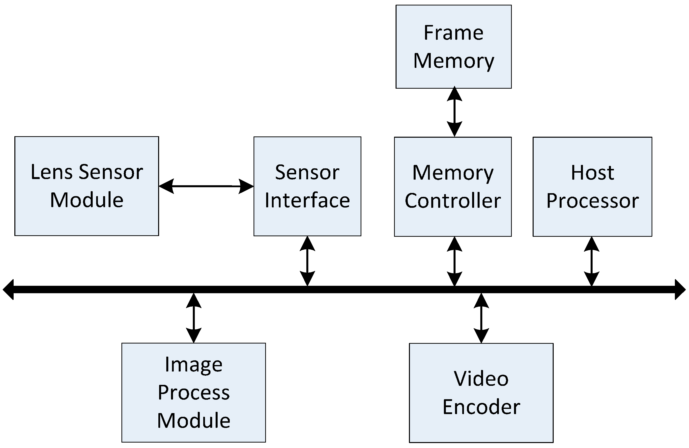
Figure 1 gives the block diagram of a video-acquisition system [
2]. The sensor interface obtains pixels from the image sensor (Lens Sensor Module) and continuously transfers them to the external memory (Frame Memory) via the memory controller. The type of the external memory is DDR3 memory with 64-bits bus width, 4GB capacity and 800 MHz memory clock frequency. Once one row of pixel-blocks in an image is ready in the external memory, the image process module processes these pixel-blocks one by one. The output pixel-block can be transferred to a typical video encoder module for video compression. The host processor (e.g., an ARM processor) is used to control or configure the other modules.
Figure 1.
Block diagram of a video-acquisition system.
Figure 1.
Block diagram of a video-acquisition system.
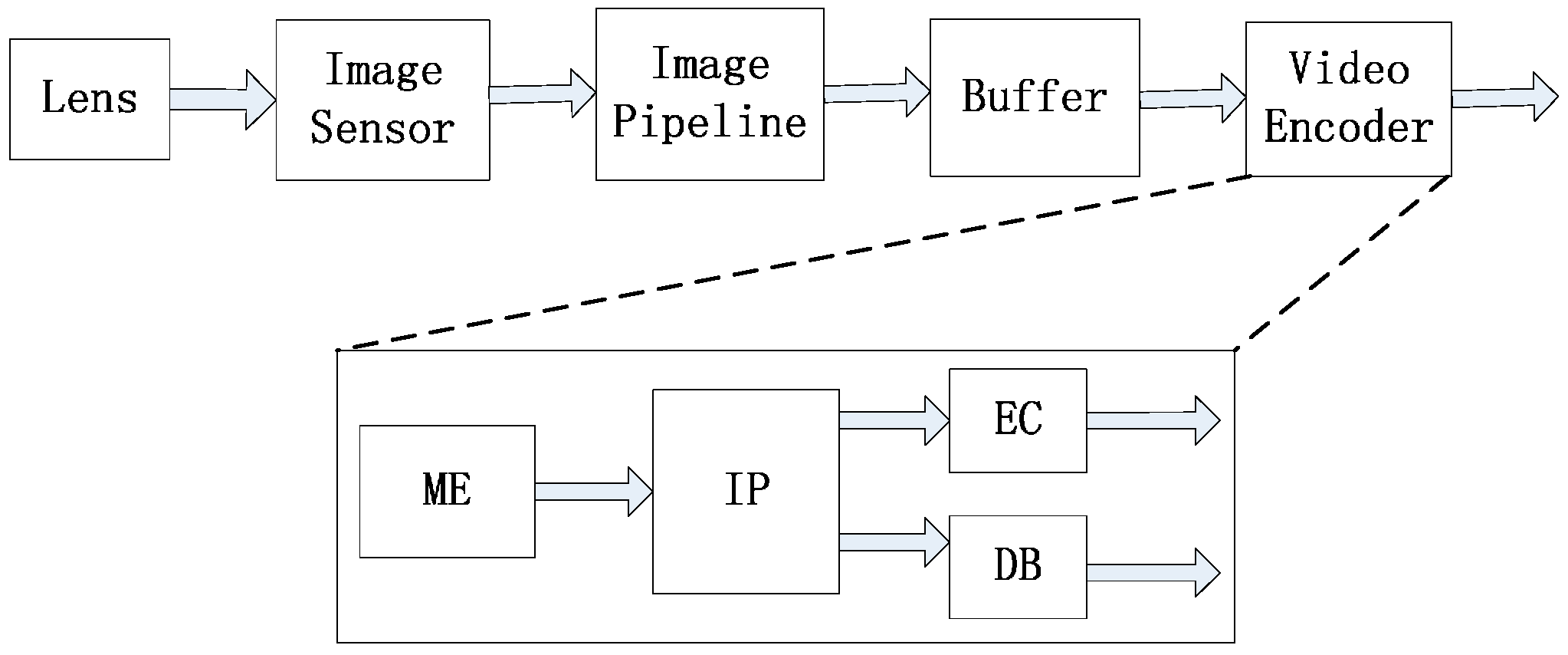
Figure 2 shows the data flow for a video-acquisition system mainly including an image sensor with video compression. The lens and image sensor are used to acquire the raw image. The image pipeline processes the pixels from the image sensor to restore vivid videos. A buffer is used to reorder line scan pixels to block scan ones. The video encoder compresses the video from the buffer and output the compressed Bitstream for transmission. In the video encoder, ME is used to reduce temporal redundancy among adjacent frames for video compression (VC-ME) [
3].
Figure 2.
Data flow for a video-acquisition system mainly including an image sensor, an image processing pipeline and a video encoder for video compression.
Figure 2.
Data flow for a video-acquisition system mainly including an image sensor, an image processing pipeline and a video encoder for video compression.
There are many ME implementations on various platforms (embedded systems, GPU and FPGA) for different types of ME, such as gradient-based, energy-based and block-based [
4,
5,
6,
7,
8,
9,
10,
11,
12,
13]. There are a lot of works for accelerating ME based on specific hardware. A novel customizable architecture of a neuromorphic robust optical flow (multichannel gradient model) is proposed in [
4], which is based on reconfigurable hardware with the properties of the cortical motion pathway. A complete quantization study of neuromorphic robust optical flow architecture is performed in [
5], using properties found in the cortical motion pathway. This architecture is designed for VLSI systems. An extensive analysis is performed to avoid compromising the viability and the robustness of the final system. A robust gradient-based optical flow model is efficiently implemented in a low-power platform based on a multi-core digital signal processor (DSP) [
6]. Graphics processor units (GPUs) offer high performance and power efficiency for a large number of data-parallel applications. Therefore, there are also many works using GPU or multi-GPU to accelerate motion estimation [
7,
8]. FPGA is also a very useful platform to accelerate motion estimation [
9,
10]. There is also a novel bioinspired sensor based on the synergy between optical flow and orthogonal variant moments; the bioinspired sensor has been designed for VLSI and implemented on FPGA [
9]. A tensor-based optical flow algorithm is developed and implemented using field programmable gate array (FPGA) technology [
10].
Block-based ME is popular for its simplicity and efficiency, and there are also many hardware-based block-matching algorithms [
11,
12,
13]. Block matching is used to find the best matching macro-block (MB) in the reference frame with the current MB. The sum of absolute differences (SAD) is one way to determine the best match. The displacement between the current MB and the best matching reference MB is the motion vector (MV). ME usually takes most of the time in VC and the accuracy of ME affects the compression ratio in VC. Full search integer ME (FSIME) employs brute-force search to find the optimal MB in the search range and achieves the best accuracy. FSIME is suitable for efficient hardware implementation because of its regularity but it demands a large number of computations and memory accesses. Therefore, it is important to reduce the time cost of VC-ME in VSN. Fast search methods are proposed to reduce time overhead usually with loss of accuracy, such as Three Step Search [
14], New Three Step Search [
15], Diamond Search [
16,
17] and Four Step Search [
18]. Fast search methods may not find the optimal MB and many of them are not regular for hardware implementation. We focus on FSIME in this paper.
In recent years, the speed gap between on-chip computing and off-chip memory access has grown larger and larger, so it is important to reduce off-chip bandwidth requirement to improve overall performance especially for real-time video applications [
19]. Reusing data on chip is usually considered to reduce off-chip memory traffic. Some data reuse methods are proposed for FSIME [
20,
21,
22,
23,
24]. Previous work mainly focused on intra-frame data reuse within a reference frame but inter-frame data reuse was neglected. For VC-ME, the reconstructed frame was usually stored to off-chip memory and then loaded to on-chip memory when needed [
23,
25,
26,
27,
28]. If the reconstructed frame is reused on chip without being stored to off-chip memory for VC-ME, the off-chip memory traffic will be greatly reduced.
In this paper, we propose a high-performance motion estimation to reduce the time cost for image sensors with video compression. The new method exploits inter-frame data reuse with affordable on-chip memory size for FSIME. The inter-frame data reuse scheme can effectively reduce off-chip memory traffic. For VC-ME, reconstructed frames are stored on chip until it is used by the next current frame. Three levels (Inter-E, Inter-D, Inter-C) of the proposed inter-frame data reuse scheme are presented and analyzed, which gives a good tradeoff between data reuse efficiency and on-chip memory size. All the three levels have better data reuse efficiency than their intra-frame counterparts. Furthermore, the new method is compatible with different intra-frame data reuse schemes [
20,
21] and scan orders [
22,
23]. Comparing the inter-frame data reuse scheme with the intra-frame data reuse scheme, we find that the memory traffic can be reduced by 50% for VC-ME according to the case study.
The rest of the paper is organized as follows: the parallelism and data locality of FSIME are analyzed in
Section 2; three levels of inter-frame data reuse scheme for VC-ME are proposed and analyzed in
Section 3; an implementation of the inter-frame data reuse architecture is presented in
Section 4; experiment results are given in
Section 5; and
Section 6 is the conclusion.
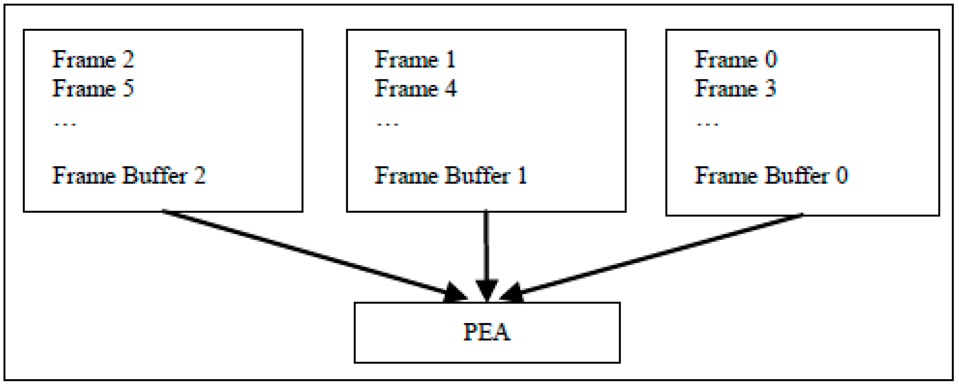
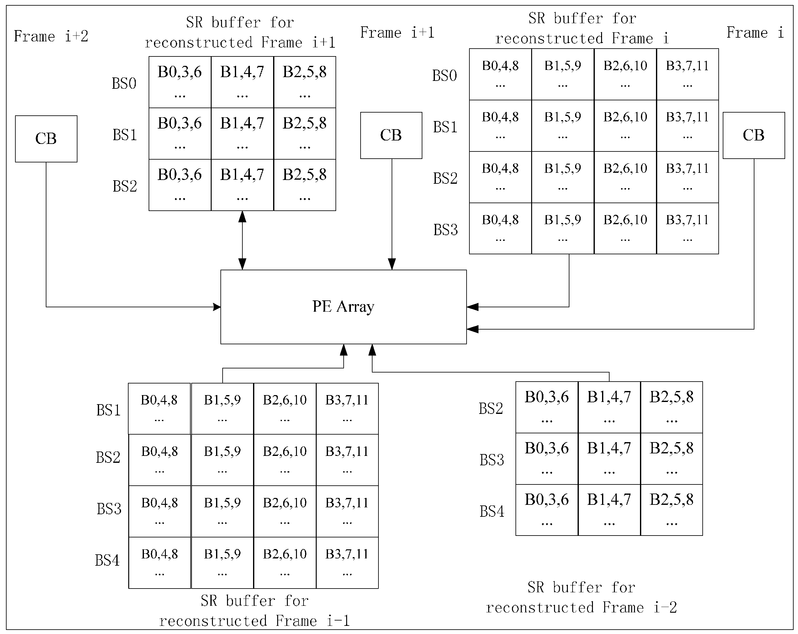
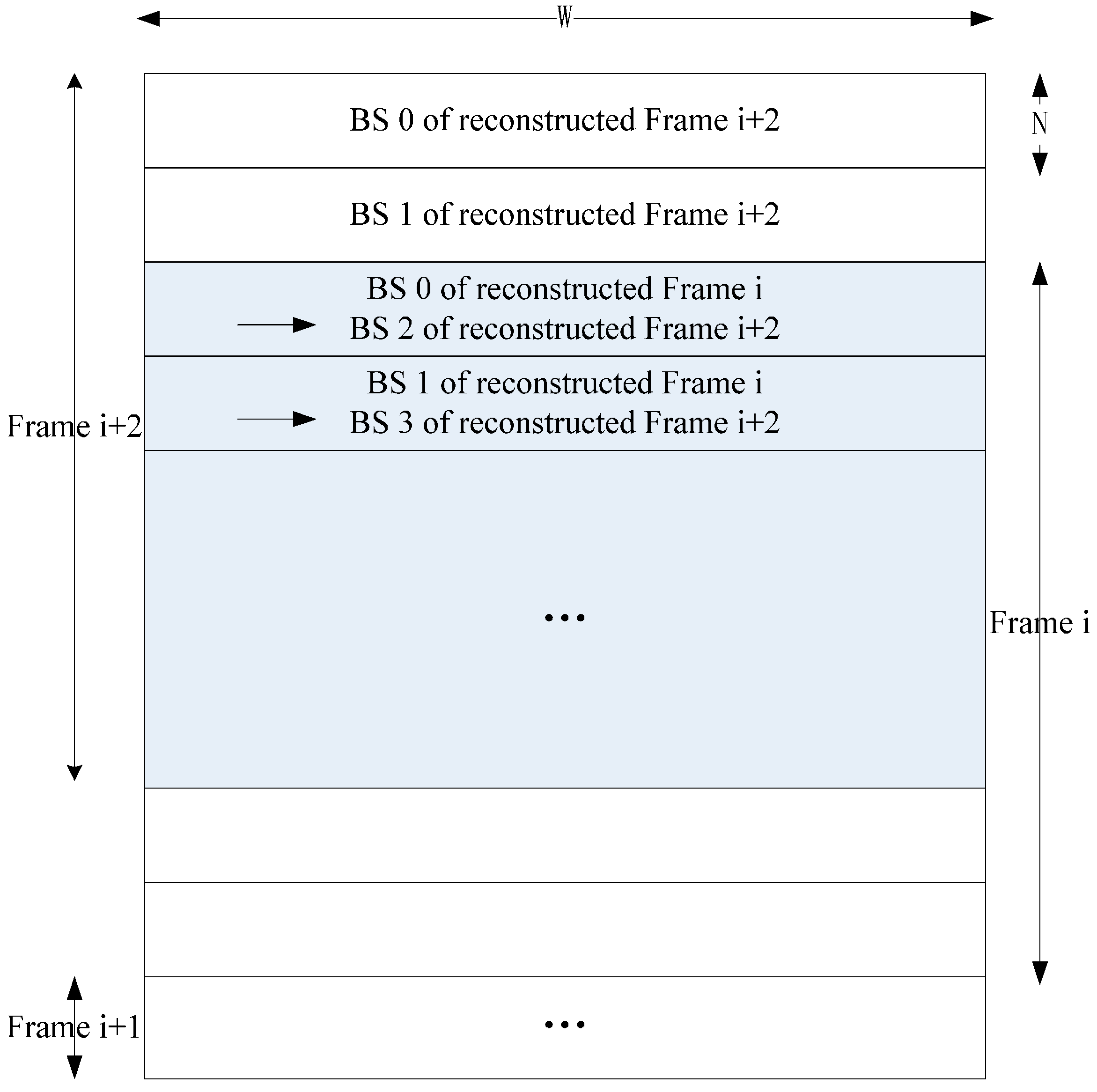
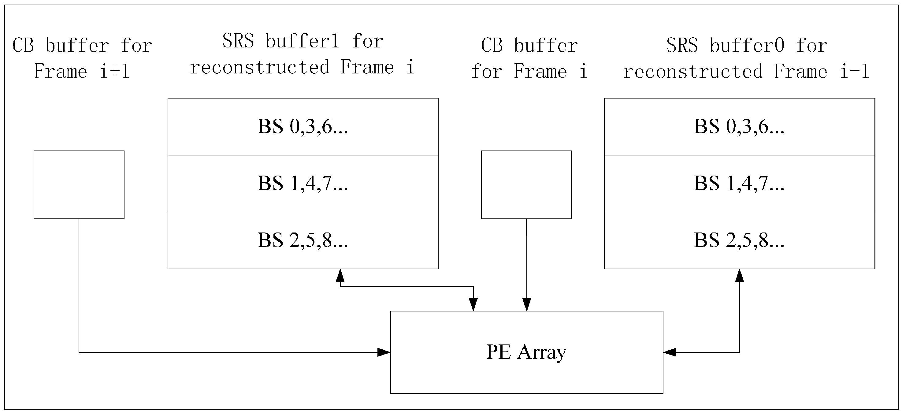
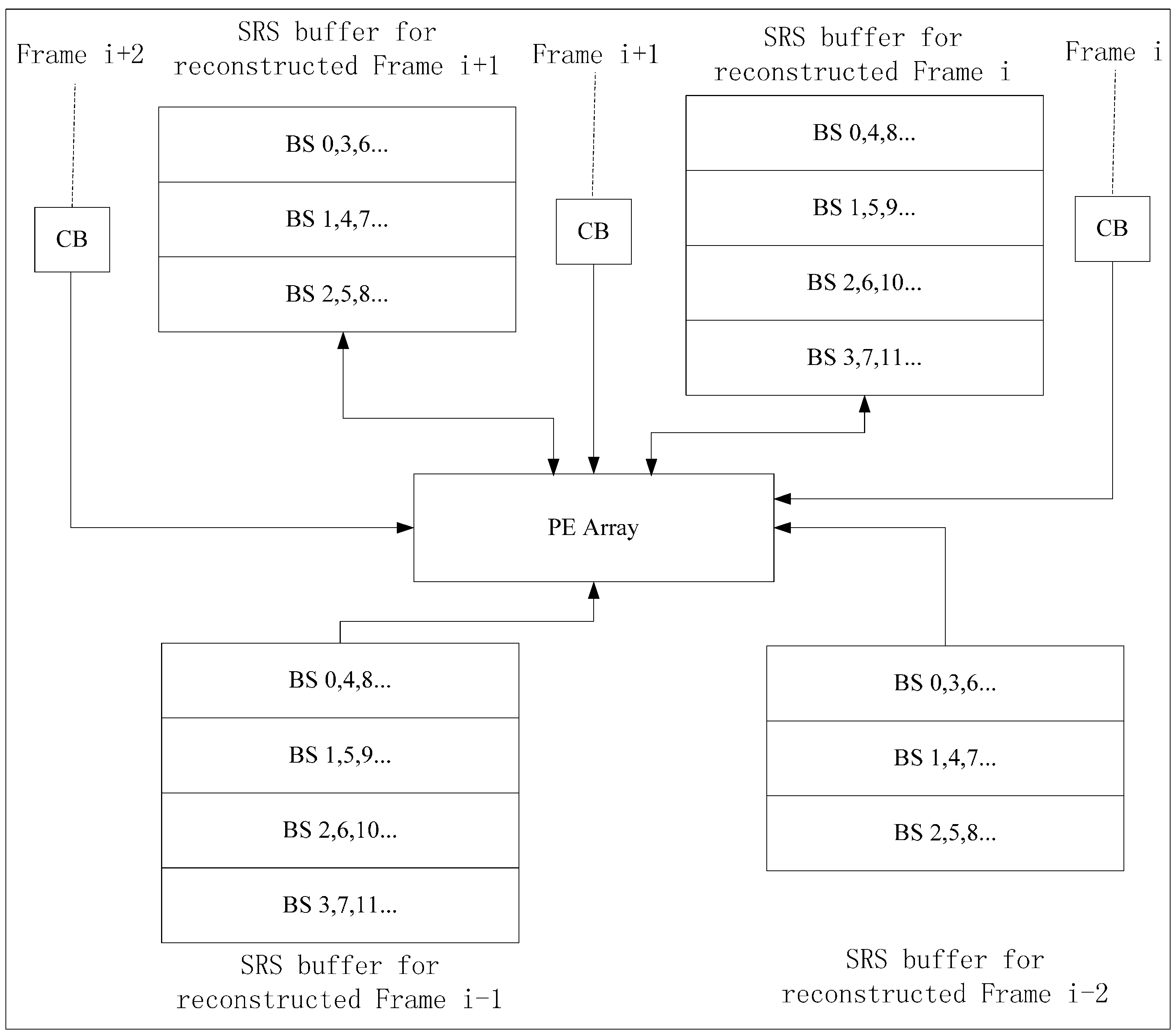
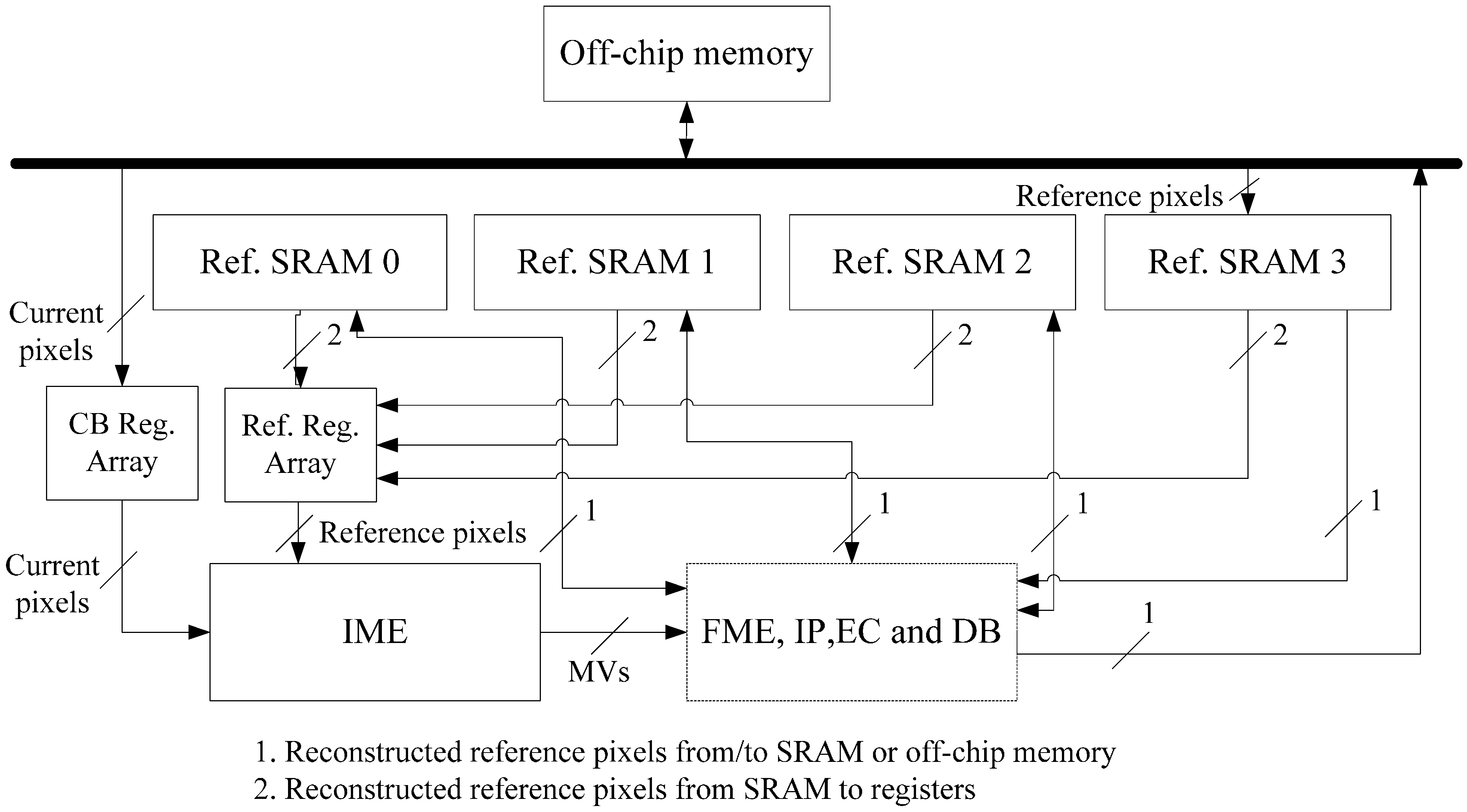
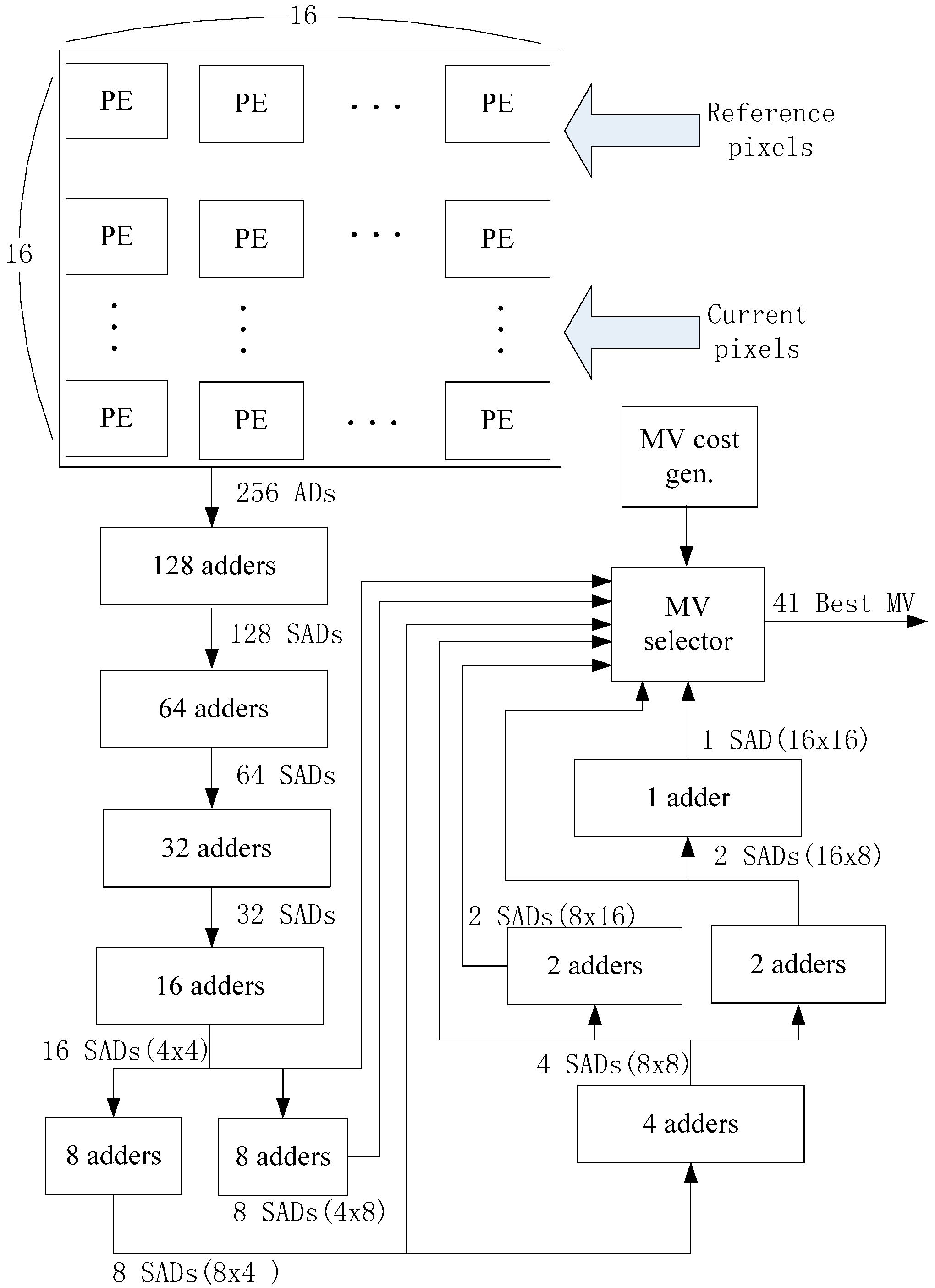
4. Implementation of Inter-D for VC-SRME
Inter-D gives a useful tradeoff between off-chip memory traffic and on-chip memory size so we implement an Inter-D architecture for VC-SRME (
Figure 18) with
m = 4. The IME module in this implementation (
Figure 19) mainly comprises of one SAD Tree [
15] with a MV selector (41 SAD comparators), which can support variable block size ME. FME, IP, EC and DB are the other modules for a complete encoder architecture but these modules are not included in our implementation. Fractional ME (FME) is usually the module after IME in an encoding pipeline. Instead of having its own on-chip buffer, FME can load data directly from IME buffer [
31], so the proposed data reuse scheme is compatible with FME. CB Reg. Array is a 16 × 16 register array which is used to store the current block. A two-level memory hierarchy is implemented between IME and off-chip memory for loading reference pixels. The first level is a 16 × 16 Ref. Reg. Array which employs Intra-A. The Ref. Reg. Array receives reference pixels from four Ref. SRAMs alternately as described in
Figure 11. The second level is four Ref. SRAMs which are used to employ Inter-D. Only Ref. SRAM 3 receives reference pixels from off-chip memory and other Ref. SRAMs all receive reference pixels which are produced on chip to reduce the off-chip memory traffic.
We implement the Inter-D VC-SRME architecture with synthesizable Verilog HDL and list synthesis results using a TSMC 65 GP technology with 360 MHz (
Table 6).
Figure 20 gives the picture of the implemented ME module in 65 nm. The proposed architecture is compared with other FSIME architectures using intra-frame data reuse. All the works in
Table 6 use full search (FS) with the frame rate of 30 f/s and the block size of 16 × 16 but they support different resolutions, SR or numbers of reference frames. The reuse level (off-chip to on-chip) affects the off-chip memory bandwidth requirement. Our implementation adopts Inter-D data reuse so it achieves the best off-chip memory access efficiency. However, the off-chip bandwidth is not only related with the data reuse level (Inter-D in the proposed architecture or Intra-D in [
29]) but also related with other parameters such as resolution, frame rate, SR, N and so on. Some of these parameters are different between [
29] and our work so the off-chip bandwidth of our work (Inter-D) is greater than that of [
29] (Intra-D). If the parameters are all the same for the two works, Inter-D will only need half the off-chip memory traffic of Intra-D. In
Section 5, we will give the comparison between the proposed Inter-D and Intra-D [
29] under the same parameters. The reuse level (on-chip) represents the reuse level from SRAM to registers on chip and affects on-chip memory bandwidth requirement. The reference [
32] proposed a novel data reuse method “Inter-candidate + Inter-macroblock” to reduce the on-chip memory bandwidth to 5 GByte/s. This method can be regarded as improved Intra-A or Inter-A. However, the goal of our proposed method is to reduce the off-chip memory traffic which is usually the performance bottleneck. The proposed inter-frame data reuse methods in this paper are compatible with “Inter-candidate + Inter-macroblock”. So we simply use a Level A data reuse with “Inter-candidate + Inter-macroblock” for reducing on-chip memory bandwidth. Note that some implementations [
25,
29] in
Table 6 only consider the memory traffic of loading the reference frame when computing off-chip or on-chip bandwidth requirement and neglect the memory traffic of loading current frames or storing reference frames. Both Level A parallelism and Level B parallelism (eight SAD Tree) are implemented in [
25] while only Level A parallelism (one SAD Tree) is implemented in our design. The gate count increases as the parallelism level increases because more PEAs are used. Due to the fact we use an Inter-D data reuse, the implementation demands a larger on-chip SRAM size (241.92 KB) than the other three works.
Figure 18.
The implemented architecture for Inter-D VC-SRME.
Figure 18.
The implemented architecture for Inter-D VC-SRME.
Figure 19.
The implemented architecture for IME.
Figure 19.
The implemented architecture for IME.
Table 6.
Comparison between Different FSIME Implementations.
Table 6.
Comparison between Different FSIME Implementations.
| | This Work | [29] | [25] | [32] |
|---|
| Search method | FS | FS | FS | FS |
| Resolution | 1920 × 1080 | 720 × 576 | 720 × 480 | 1920 × 1088 |
| Frame rate | 30 fps | 30 fps | 30 fps | 30 fps |
| Reference frames | 1 | 2 | 4 | 1 |
| SR | 32 × 32 | 65 × 33 | 128 × 64, 64 × 32 | 32 × 32 |
| N | 16 | 16 | 16 | 16 |
| Reuse level(off-chip to on-chip) | Inter-D | Intra-D | Intra-C | Intra-C |
| Reuse level (on-chip) | Intra-A | Intra-A | Intra-A | Intra-A |
| Parallelism level | A | A | A,B | A,B,C |
| Off-chip bandwidth (MByte/s) | 93.31 | 24.9 | 135.9 | 319 |
| On-chip bandwidth (MByte/s) | 5120 | - | - | 5120 |
| Technology | 65 nm | 0.18 um | 0.18 um | 0.18 um |
| Frequency (MHz) | 360 | 216 | 81 | 130 |
| Gate count (K) | 166 | 168 | 330 | 1449 |
| SRAM (KB) | 241.92 | 23.75 | 26 | 1.26 |
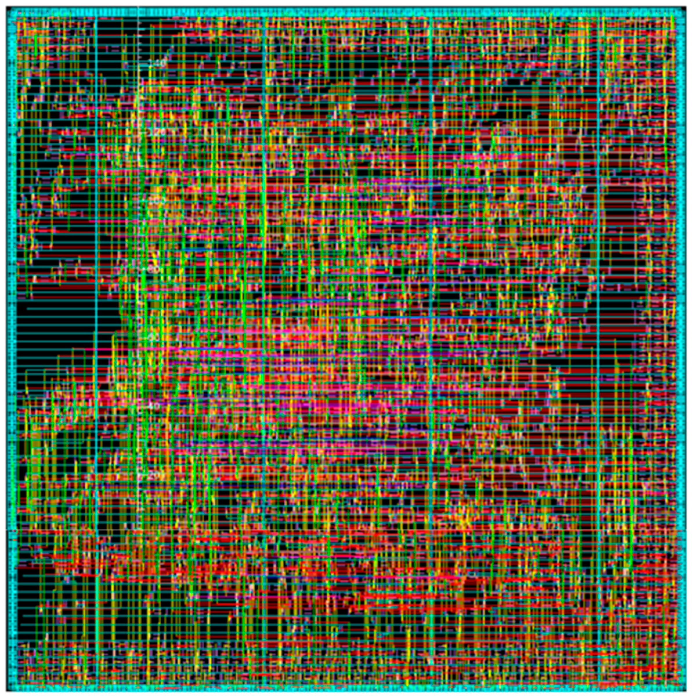
Figure 20.
Picture of the implemented ME module in 65 nm.
Figure 20.
Picture of the implemented ME module in 65 nm.
5. Experiment Results
We give three case studies (1080 p, 720 p and 4 K) to analyze and compare different data reuse levels for VC-ME. Ra and on-chip memory size of two different application scenarios are computed according to
Table 4 and
Table 5 respectively, where m and n both equals 4. Intra-A, Intra-B, Intra-C, Intra-D, and Inter-E are traditional data reuse methods. Inter-A, Inter-B, Inter-C, Inter-D and New Inter-E are proposed inter-frame data reuse methods. Bandwidth in Equation (8) is the off-chip memory bandwidth requirement. f is frame rate.
For VC-SRME (
Table 7), the bandwidth requirement reductions of Inter-D are 50% compared with Intra-D [
29], which is the largest memory traffic reduction ratio for VC-SRME. Inter-E needs 4.1 MB on-chip memory for 1080 p, 1.8 MB for 720 p and 16.6 MB for 4 K, and the on-chip memory size is reduced nearly by half after using the proposed circular frame buffer (New Inter-E) while the bandwidth requirement is the same. Compared with no data reuse, Intra-A [
20] and Intra-B [
20] can reduce a large amount of memory traffic with a small on-chip memory size. However, they still demand too much memory bandwidth. The proposed three inter-frame data reuse schemes all have better data reuse efficiency than their intra-frame counterparts for all the three specifications. For 1080p and 4K, the bandwidth requirement reductions of Inter-C, Inter-C+, and Inter-D are 15%, 21.4%, and 50% respectively, compared with Intra-C [
25,
29], Intra-C+ [
21], and Intra-D. For 720 p, the bandwidth requirement reductions of Inter-C, Inter-C+, and Inter-D are 18.8%, 23.1%, and 50% respectively, compared with Intra-C, Intra-C+, and Intra-D.
Table 7.
Three Case Studies for VC-SRME.
Table 7.
Three Case Studies for VC-SRME.
| Reuse Level | 1080 p, 30 fps, | 720 p, 30 fps, | 4 K, 60 fps, |
|---|
| SRH = SRV = 32, N = 16 | SRH = SRV = 16, N = 16 | SRH = SRV = 128, N = 64 |
|---|
| | Ra | Bandwidth (MByte/s) | On-Chip Memory Size (KB) | Ra | Bandwidth (MByte/s) | On-Chip Memory Size (KB) | Ra | Bandwidth (MByte/s) | On-Chip Memory Size (KB) |
|---|
| No reuse | 1026 | 63,825.4 | 0 | 258 | 7133.2 | 0 | 16,386 | 8,154,722.3 | 0 |
| Intra-A | 98 | 6096.4 | 0.24 | 34 | 940.0 | 0.24 | 386 | 192,098.3 | 4.03 |
| Intra-B | 11 | 684.3 | 0.72 | 6 | 165.9 | 0.48 | 11 | 5474.3 | 12.10 |
| Intra-C | 5 | 311.0 | 2.21 | 4 | 110.6 | 0.96 | 5 | 2488.3 | 36.48 |
| Inter-C | 4.25 | 264.4 | 8.84 | 3.25 | 89.9 | 3.84 | 4.25 | 2115.1 | 145.92 |
| Intra-C+ | 3.5 | 217.7 | 4.47 | 3.25 | 89.9 | 2.45 | 3.5 | 1741.8 | 73.15 |
| Inter-C+ | 2.75 | 171.1 | 17.86 | 2.5 | 69.1 | 9.80 | 2.75 | 1368.6 | 292.61 |
| Intra-D | 3 | 186.6 | 60.48 | 3 | 82.9 | 19.43 | 3 | 1493.0 | 503.81 |
| Inter-D | 1.5 | 93.3 | 241.92 | 1.5 | 41.5 | 77.72 | 1.5 | 746.5 | 2015.24 |
| Inter-E | 1 | 62.2 | 4147.20 | 1 | 27.7 | 1843.20 | 1 | 497.7 | 16,588.80 |
| New Inter-E | 1 | 62.2 | 2135.04 | 1 | 27.7 | 962.56 | 1 | 497.7 | 8785.92 |
For VC-MRME (
Table 8), the video sequence is encoded with one I frame initially and the following frames are all encoded using the previously encoded and reconstructed r frames. r equals 4 in this case study. The on-chip memory size is r times of VC-SRME for the corresponding intra-frame data reuse level because it has to keep r buffers for r reference frames. Compared with no data reuse, Intra-A and Intra-B can reduce a large amount of memory traffic with a small on-chip memory size. However, they still demand too much memory bandwidth, 24.0 GByte/s and 2.4 GByte/sec for Intra-A and Intra-B, respectively. For 1080 p and 4 K, the bandwidth requirement reductions of Inter-C, Inter-C+, and Inter-D are 37.5%, 30.6%, and 50% respectively, compared with their intra-frame counterparts. For 720 p, the bandwidth requirement reductions of Inter-C, Inter-C+, and Inter-D are 30%, 18.8%, and 50% respectively, compared with their intra-frame counterparts.
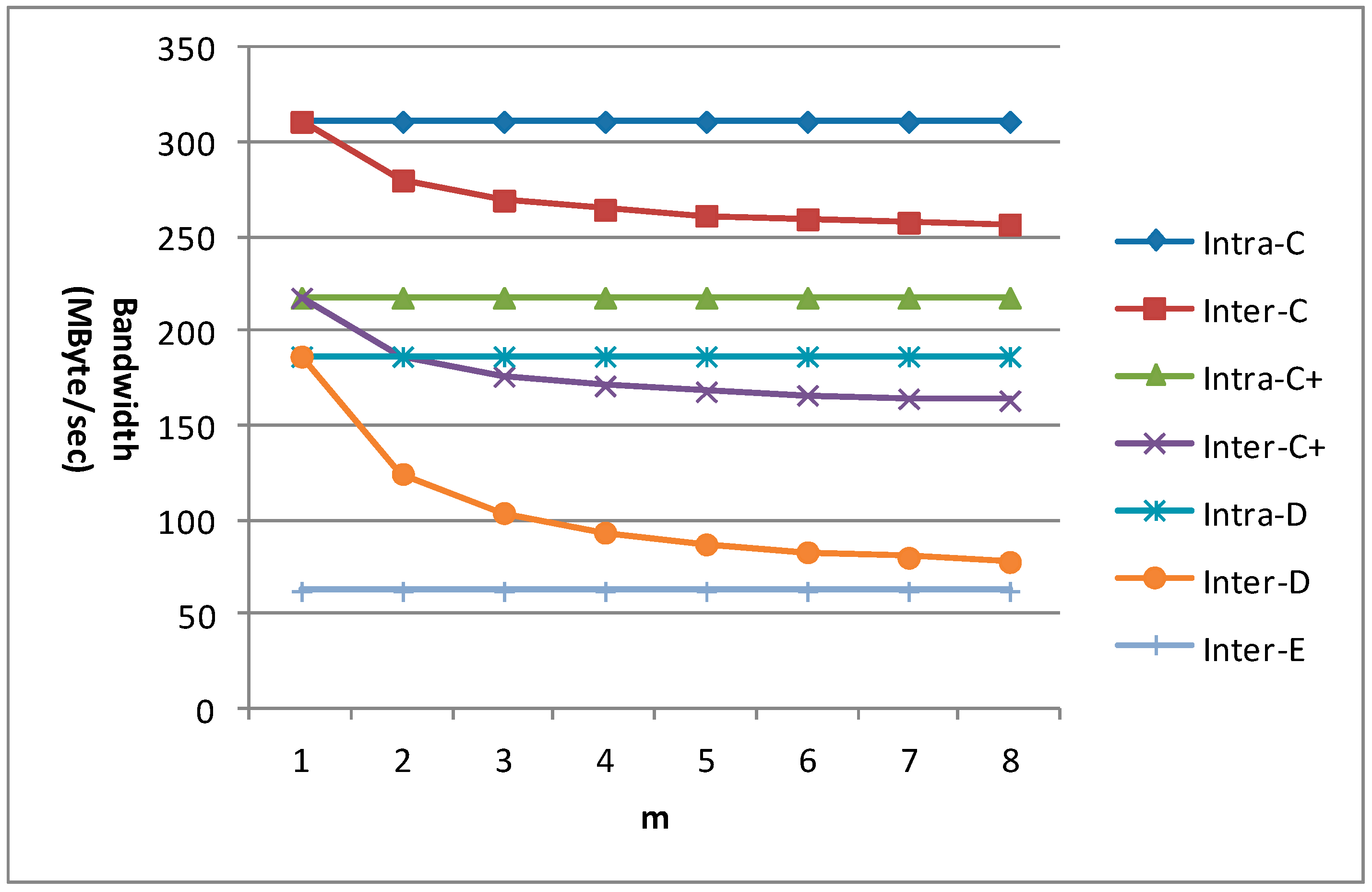
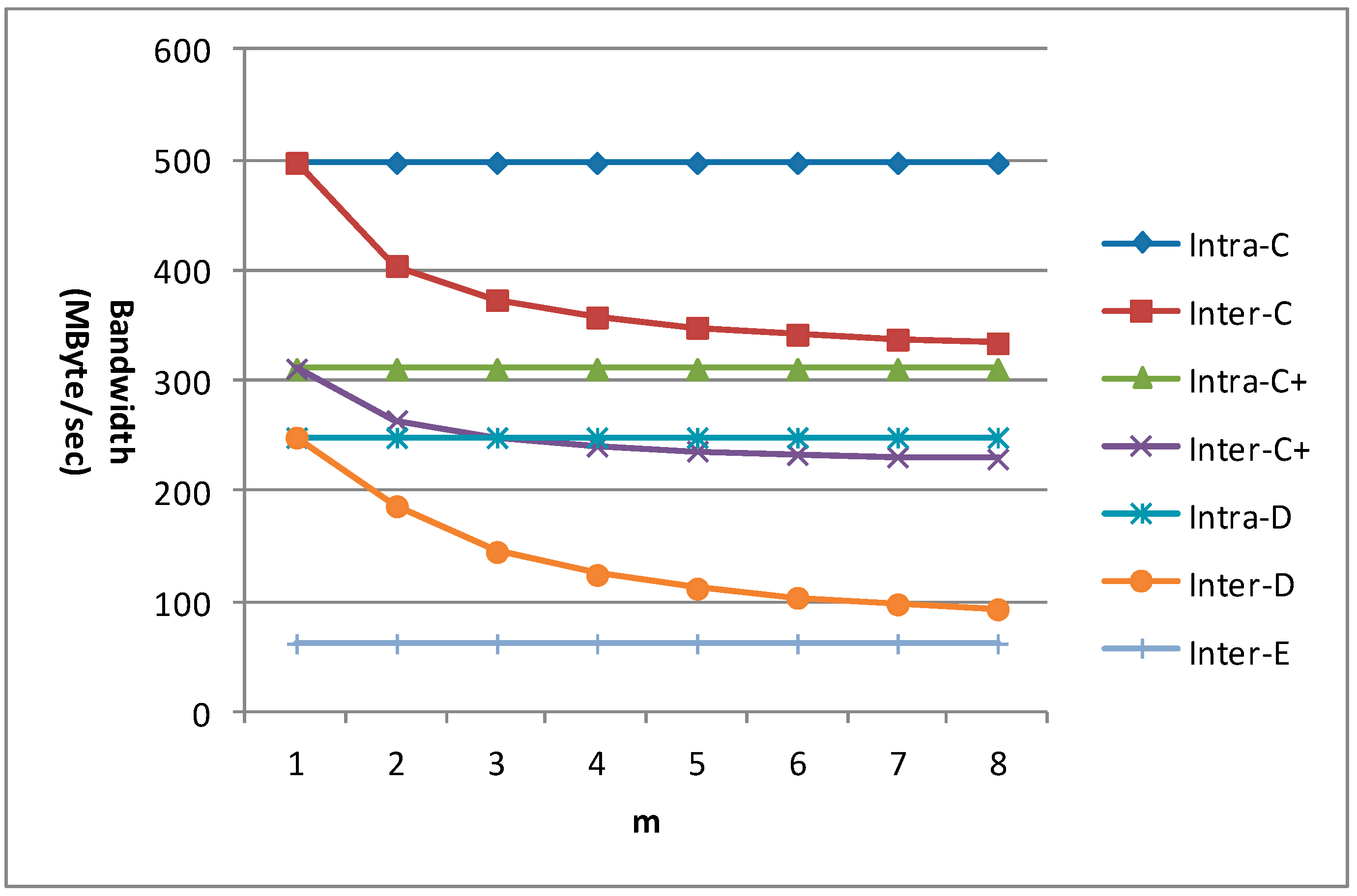
m is an important factor which affects the data reuse efficiency for the new inter-frame data reuse scheme. So the bandwidth requirement for 1080 p with different m is given in
Figure 21 for different data reuse levels of VC-SRME. n equals 4 in the C+ scheme. We can find that the bandwidth requirements of all the intra-frame data reuse levels (including Intra-A and Intra-B which are not shown in the figure) and Inter-E are unchanged with the variation of m. When m equals 1, the bandwidth requirement of the inter-frame data reuse level is the same as that of its corresponding intra-frame data reuse level. The bandwidth requirements of Inter-C, Inter-C+, and Inter-D become lower with the increase of m, but the bandwidth reduction magnitude becomes smaller because there is always a constant which will not change with m in the formula of Ra. We find that the bandwidth requirement reduction for Inter-D is more effective than that for Inter-C or Inter-C+ because Inter-D can reuse the reconstructed frame more efficiently.
Table 8.
Three Case Studies for VC-MRME.
Table 8.
Three Case Studies for VC-MRME.
| Reuse Level | 1080 p, 30 fps, SRH = SRV = 32, N = 16 | 720 p, 30 fps, SRH = SRV = 16, N = 16 | 4 K, 60 fps, SRH = SRV = 128, N = 64 |
|---|
| | Ra | Bandwidth (MByte/s) | On-Chip Memory Size(KB) | Ra | Bandwidth (MByte/s) | On-Chip Memory Size(KB) | Ra | Bandwidth (MByte/s) | On-Chip Memory Size(KB) |
|---|
| No reuse | 4098 | 254,928.4 | 0 | 1026 | 28,366.9 | 0 | 65538 | 32,615,903.2 | 0 |
| Intra-A | 386 | 24,012.3 | 0.96 | 130 | 3594.2 | 0.96 | 1538 | 765,407.2 | 16.13 |
| Intra-B | 38 | 2363.9 | 2.88 | 18 | 497.7 | 1.92 | 38 | 18,911.2 | 48.38 |
| Intra-C | 14 | 870.9 | 8.84 | 10 | 276.5 | 3.84 | 14 | 6967.3 | 145.92 |
| Inter-C | 8.75 | 544.3 | 33.86 | 7 | 193.5 | 20.52 | 8.75 | 4354. 6 | 553.22 |
| Intra-C+ | 8 | 497.7 | 17.86 | 7 | 193.5 | 9.80 | 8 | 3981.3 | 292.61 |
| Inter-C+ | 6.125 | 381.0 | 56.57 | 5.6875 | 157.3 | 37.85 | 6.125 | 3048.2 | 920.52 |
| Intra-D | 6 | 373.3 | 241.92 | 6 | 165.9 | 77.70 | 6 | 2986.0 | 2015.24 |
| Inter-D | 3 | 186.6 | 922.82 | 3 | 82.9 | 467.50 | 3 | 1493.0 | 7588.87 |
| Inter-E | 1 | 62.2 | 10,368.00 | 1 | 27.7 | 4608.00 | 1 | 497.7 | 41,472.00 |
| New Inter-E | 1 | 62.2 | 8355.84 | 1 | 27.7 | 3727.36 | 1 | 497.7 | 33,669.12 |
Figure 21.
The bandwidth requirement of VC-SRME for 1080 p.
Figure 21.
The bandwidth requirement of VC-SRME for 1080 p.
The bandwidth requirement for 1080 p with different m is given in
Figure 22 for different data reuse levels of VC-MRME. n equals 4 in the C+ scheme and r equals 2. We can find that the bandwidth requirements of all the intra-frame data reuse levels (including Intra-A and Intra-B which are not shown in the figure) and Inter-E are unchanged with the variation of m. When m equals 1, the bandwidth requirement of the inter-frame data reuse level is the same as that of its corresponding intra-frame data reuse level. The bandwidth requirements of Inter-C, Inter-C+, and Inter-D become lower with the increase of m, but the bandwidth reduction magnitude becomes smaller because there is always a constant which will not change with m in the formula of Ra.
Figure 22.
The bandwidth requirement of VC-MRME for 1080 p.
Figure 22.
The bandwidth requirement of VC-MRME for 1080 p.
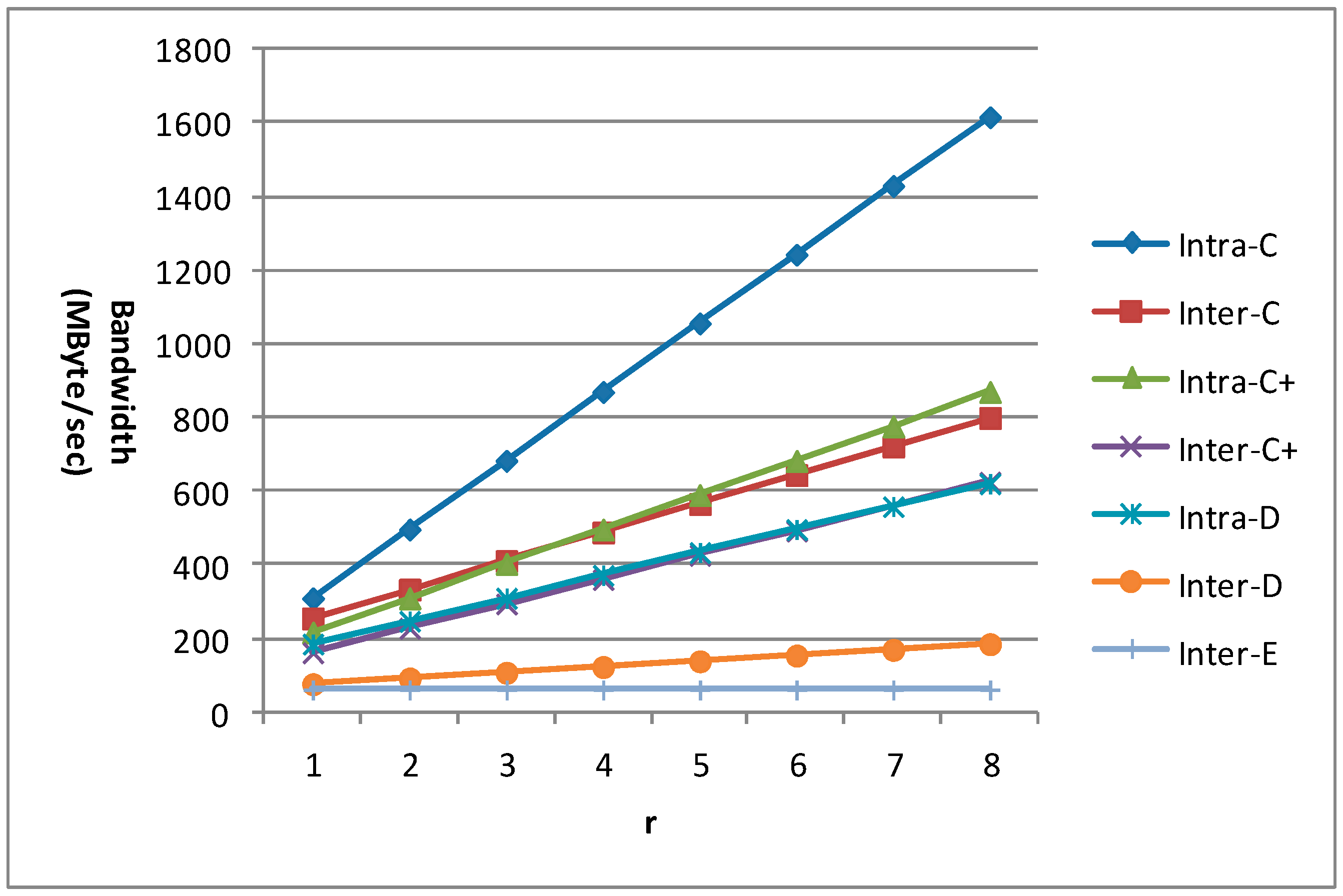
The value of r is a factor which can reflect how the number of reference frames affects the memory traffic of different data reuse levels for VC-MRME, so we give the bandwidth requirements of different values of r when n equals 4 and m equals 8 in
Figure 23. There is a linear relationship between the value of r and the bandwidth requirements of different data reuse levels, which means that a larger r will lead to more memory traffic because more data need to be loaded from off-chip memory. The slope of an intra-frame data reuse scheme is larger than that of its inter-frame counterpart, which means that memory traffic of the intra-frame data reuse increases faster with r than its inter-frame counterpart. Therefore, the proposed inter-frame data reuse scheme is more scalable than the traditional intra-frame data reuse scheme for multiple reference frames ME.
Figure 23.
The bandwidth requirement of VC-MRME for 1080 p with different values of r. n equals 4 for C+ scheme. m equals 8.
Figure 23.
The bandwidth requirement of VC-MRME for 1080 p with different values of r. n equals 4 for C+ scheme. m equals 8.
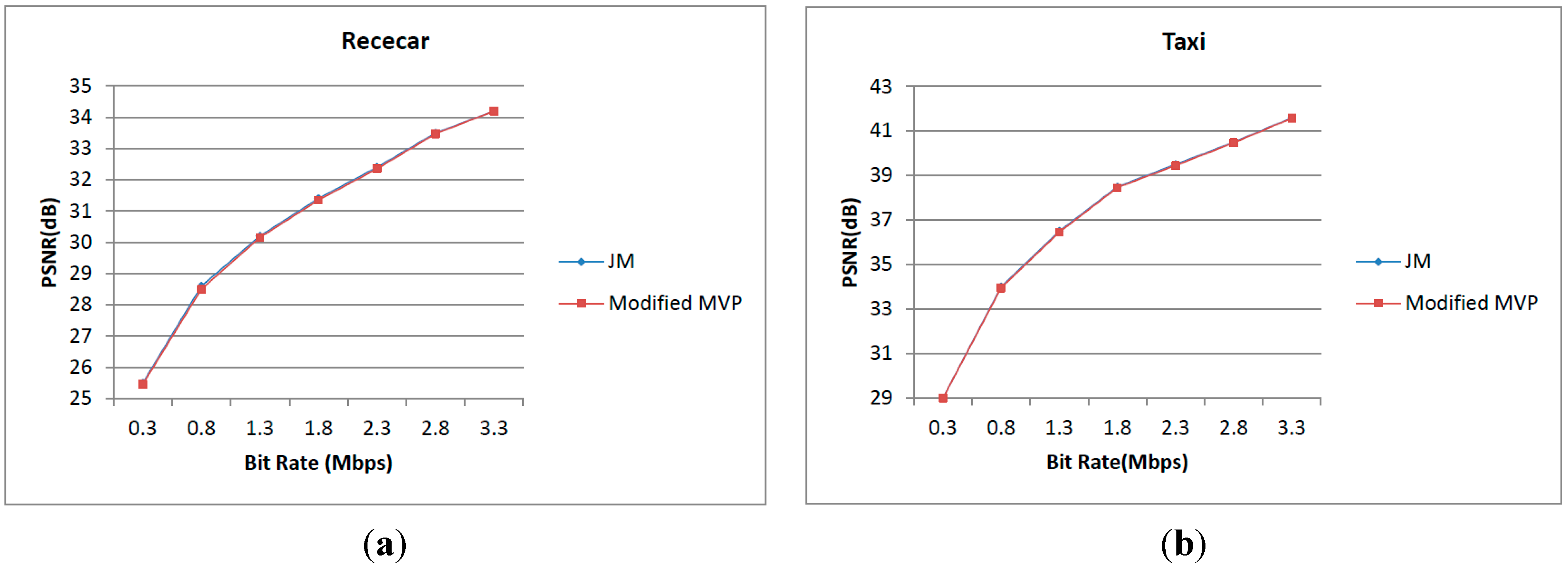
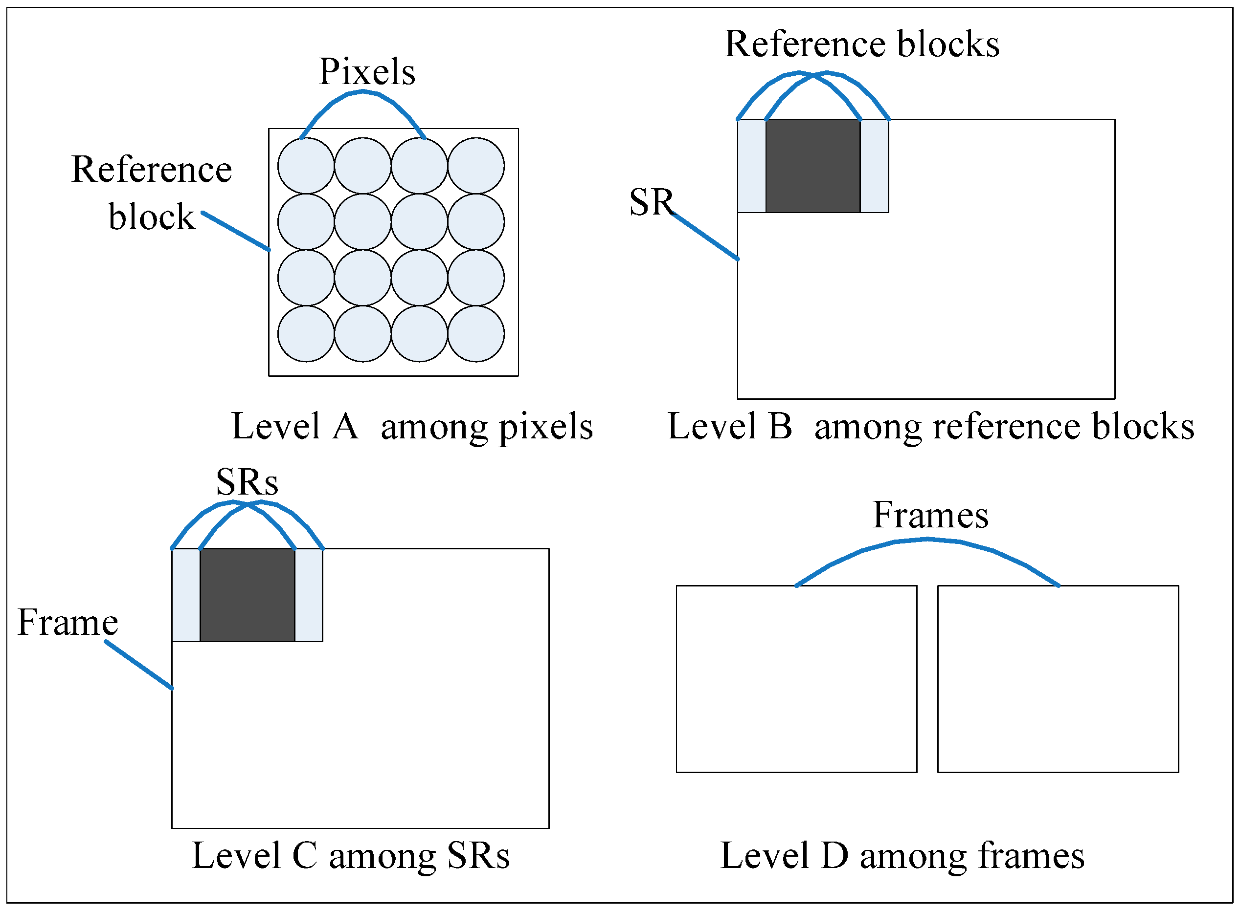
The Level C parallelism defined in
Section 2 is based on modifying the calculation of the predicted motion vector (MVP) [
25]. Therefore, the quality analysis is needed to be accomplished.
Figure 24a,b shows the comparisons of RD curves between JM and the modified motion vector prediction. Many sequences have been tested from QCIF to HDTV, and two of them are Racecar (720 × 288, 30 fps) and Taxi (672 × 288, 30 fps). From the figure, we can find that the quality loss is near zero at high bit rates (larger than 1 Mb/s) and the quality is degraded 0.1 dB at a low bit rate [
25]. We can conclude that the coding performance of the modified MVP is competitive with that of JM. For Level A and B parallelism and the proposed different data reuse levels, a standard motion vector prediction and a classical full search algorithm is used and nothing which can affect quality is modified. Therefore, the best quality can be achieved.
Figure 24.
Comparison of RD curves between JM and modified motion vector prediction. (a) The comparison between JM and modified motion vector prediction in Racecar; (b) The comparison between JM and modified motion vector prediction in Taxi.
Figure 24.
Comparison of RD curves between JM and modified motion vector prediction. (a) The comparison between JM and modified motion vector prediction in Racecar; (b) The comparison between JM and modified motion vector prediction in Taxi.
Our method can effectively reduce the number of off-chip memory accesses, which will affect positively the power consumption. We perform power consumption analysis for different data reuse schemes, Intra-C, Inter-C, Intra-C+, Inter-C+, Intra-D, and Inter-D. We model the DRAM access power according to [
33,
34]. We assume that the static power is constant with respect to accesses and evenly distributed across all banks. The dynamic power is proportional to the read bandwidth and write bandwidth. The equation for DRAM access power is as follows [
34], where BWr and BWw represent the read bandwidth and write bandwidth in GB/s.
Table 9 gives the power consumptions of the 1080 p case for VC-SRME according to
Table 7. We find that the power consumptions of the inter-frame data reuse schemes are all lower than their intra-frame counterparts.
Table 9.
Power analysis of 1080 p for VC-SRME.
Table 9.
Power analysis of 1080 p for VC-SRME.
| | BWr (GB/s) | BWw (GB/s) | P (mW) |
|---|
| Intra-C | 0.249 | 0.062 | 234.95 |
| Inter-C | 0.202 | 0.062 | 199.56 |
| Intra-C+ | 0.156 | 0.062 | 164.92 |
| Inter-C+ | 0.109 | 0.062 | 129.53 |
| Intra-D | 0.124 | 0.062 | 140.82 |
| Inter-D | 0.031 | 0.062 | 70.80 |


