
On-Chip Sensing of Thermoelectric Thin Film’s Merit

1
Department of Electrical Engineering, Alabama A&M University, Normal, AL 35762, USA
2
Department of Electrical and Biomedical Engineering, University of Nevada, Reno, NV 89557, USA
*
Author to whom correspondence should be addressed.
Sensors 2015, 15(7), 17232-17240; https://doi.org/10.3390/s150717232
Submission received: 1 May 2015
/
Revised: 19 June 2015
/
Accepted: 13 July 2015
/
Published: 16 July 2015
(This article belongs to the Section Physical Sensors)
Abstract
:Thermoelectric thin films have been widely explored for thermal-to-electrical energy conversion or solid-state cooling, because they can remove heat from integrated circuit (IC) chips or micro-electromechanical systems (MEMS) devices without involving any moving mechanical parts. In this paper, we report using silicon diode-based temperature sensors and specific thermoelectric devices to characterize the merit of thermoelectric thin films. The silicon diode temperature sensors and thermoelectric devices were fabricated using microfabrication techniques. Specifically, e-beam evaporation was used to grow the thermoelectric thin film of Sb2Te3 (100 nm thick). The Seebeck coefficient and the merit of the Sb2Te3 thin film were measured or determined. The fabrication of silicon diode temperature sensors and thermoelectric devices are compatible with the integrated circuit fabrication.
1. Introduction
Managing heat flux has been one of the most important technical challenges that the current integrated circuit (IC) or MEMS industry is facing, because the rising temperature limits the miniaturization of IC or MEMS devices and decreases their lifetime [1]. Solid-state thermoelectric (TE) cooling techniques are of great interest to solve this problem, because they can remove heat from the IC chips or MEMS devices without involving any moving mechanical parts. TE materials and devices have been extensively investigated by researchers for the application of thermal-to-electrical energy conversion or solid-state cooling [2,3,4,5,6,7,8,9,10,11,12,13,14,15,16]. However, the use of TE materials and devices is currently limited by their low efficiency. Nanostructured TE materials, such as nanolayered thin films and quantum-dot superlattices, have been found to have a thermoelectric merit significantly greater than the same bulk materials [17], due to the effect of quantum confinement on electrons and holes, as well as higher impedance to phonon transport in the nanoscale materials. The thermoelectric merit is defined as: ZT = S2σT/κ, where T is the absolute temperature, σ is the electrical conductivity, κ is the thermal conductivity, and S is the Seebeck coefficient (defined as voltage difference divided by temperature difference (ΔV/ΔT)). The figure of merit of a TE device can also be obtained by measuring the maximum temperature achieved in the device. The formula for calculating the ZT value of a TE device is: ZT = 2ΔTmax/T. It is challenging to characterize the nanoscale TE materials and accurately measure the three parameters simultaneously for finding the ZT value. On the other hand, in some TE material based devices, it is desired to frequently in-field monitor the ZT change of the TE materials in order to diagnose the device lifetime or quality degradation in use. To address these needs, two microstructures and one in-plane integrated TE device integrating temperature sensors and Sb2Te3 film, are proposed for on-chip sensing of the Seebeck Coefficient and ZT parameter (as shown in Figure 1, Figure 2 and Figure 3). To measure the cross-plane Seebeck coefficient of a TE film, the TE film is sandwiched between a diode-based temperature sensor and a Pt film temperature sensor (Figure 1). The cross-plane Seebeck coefficient is obtained by measuring the voltage difference and temperature difference between the top and bottom surface of the film. To measure the in-plane Seebeck coefficient of a TE film, the two ends of the TE film are located on the top of two diode-based temperature sensors (Figure 2). The in-plane Seebeck coefficient is obtained by measuring the voltage difference and temperature difference between the two ends of the film. To measure the ZT value of the in-plane integrated TE device, two diode-based temperature sensors are designed at the left side and the right side of the device (Figure 3). The ZT value is obtained by measuring the maximum temperature difference achieved in the TE device. These microstructures are fully compatible to IC or MEMS fabrication steps, and can be easily built in to any TE film based devices.
2. Experimental Details
We fabricated three thermoelectric (TE) devices of Sb2Te3 thin film to characterize the silicon diode temperature sensors and measure the in-plane and cross-plane Seebeck coefficient of Sb2Te3 thin film using the microfabrication techniques. The three TE devices include two single TE devices, and one integrated TE device, which consists of many TE elements. A 76-mm-diameter p-type (001) silicon wafer was used as the substrate in fabricating the TE devices. The silicon wafer has a resistivity of 1 to 5 Ω·cm. The fabrication processes included thermal wet oxidation to growing the initial oxide layer; heavily boron doping on the backside of wafer for making the ohmic contact; phosphorous doping for making the p-n junction of diode temperature sensor; depositing the SiO2 thin film for the insulation layer; depositing the Sb2Te3 thin film for making the TE element; depositing the aluminum (Al) and gold (Au) thin films for the metal contact. Thermal diffusion was used for both boron and phosphorous doping. Ultra-violet (UV) lithography was adopted for patterning in fabricating the devices. All the thin films were grown via electron-beam evaporation at room temperature without substrate heating. The substrate holder was rotated at the speed of 20 RPM during the deposition. The process chamber had a background pressure of 2 × 10⁻⁷ Torr. An INFICON deposition monitor controlled their thicknesses. Solid antimony (III) telluride (99.999% purity; Alfa Aesar Company) was used as the source material for growth of the Sb2Te3 thin film. The deposition pressure was 1 × 10⁻⁶ Torr, and the growth rate was 1 Å/s. The film was prepared as 100 nm thick. The E-beam-evaporation-grown antimony telluride film can have the desired stoichiometry of Sb2Te3 [18]. A 50 nm-thick gold (Au) layer was deposited for the metal contact of the Sb2Te3 film. A 100-nm-thick platinum (Pt) layer was grown for fabricating the Pt Serpentine-resistor temperature sensor. The fabricated device wafer was annealed at 200 °C for 30 min before the measurements. The devices were imaged in a scanning electron microscope. All the electrical measurements were performed under the vacuum condition of 5 × 10⁻⁴ Torr.
3. Results and Discussion
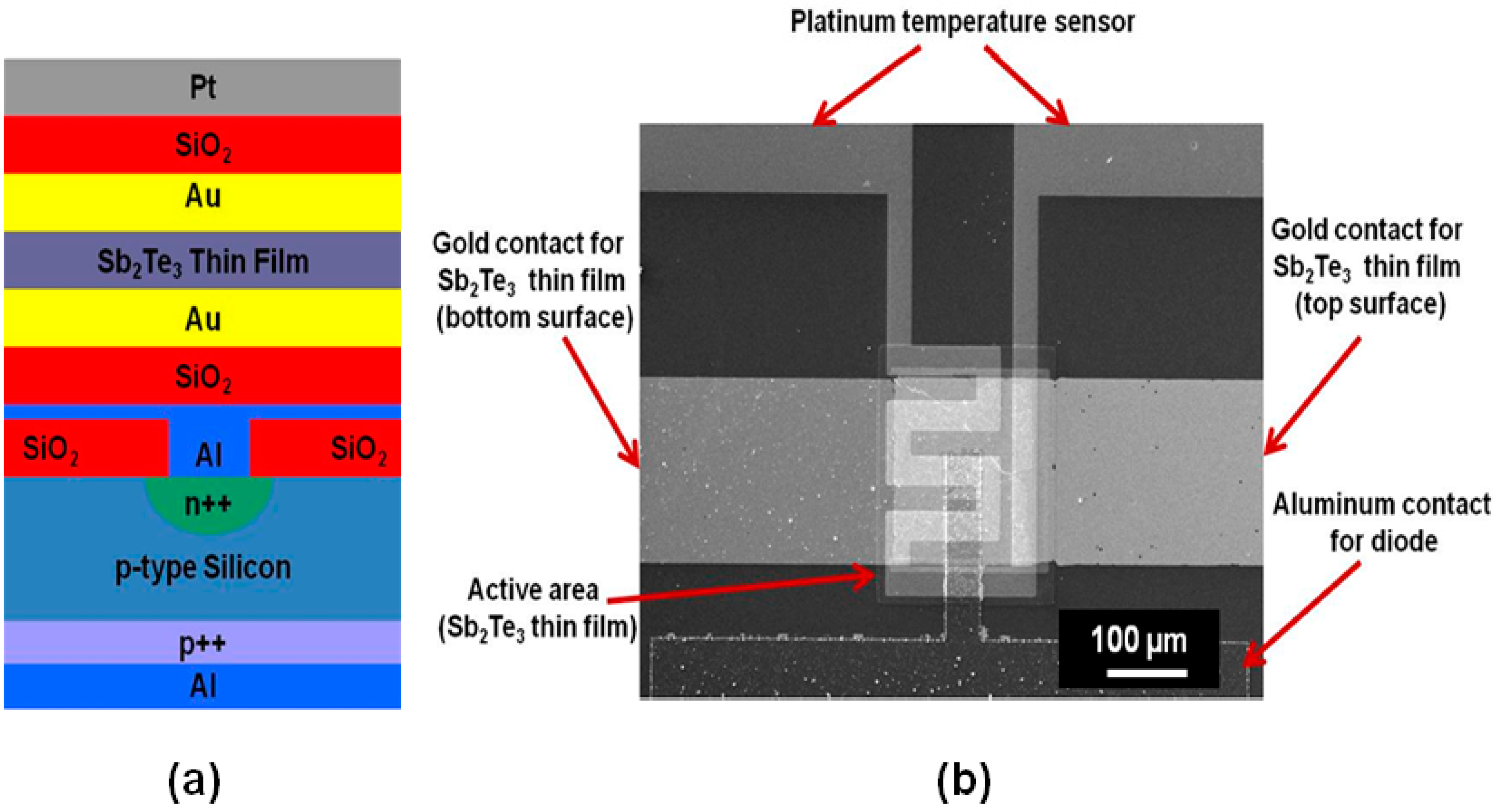
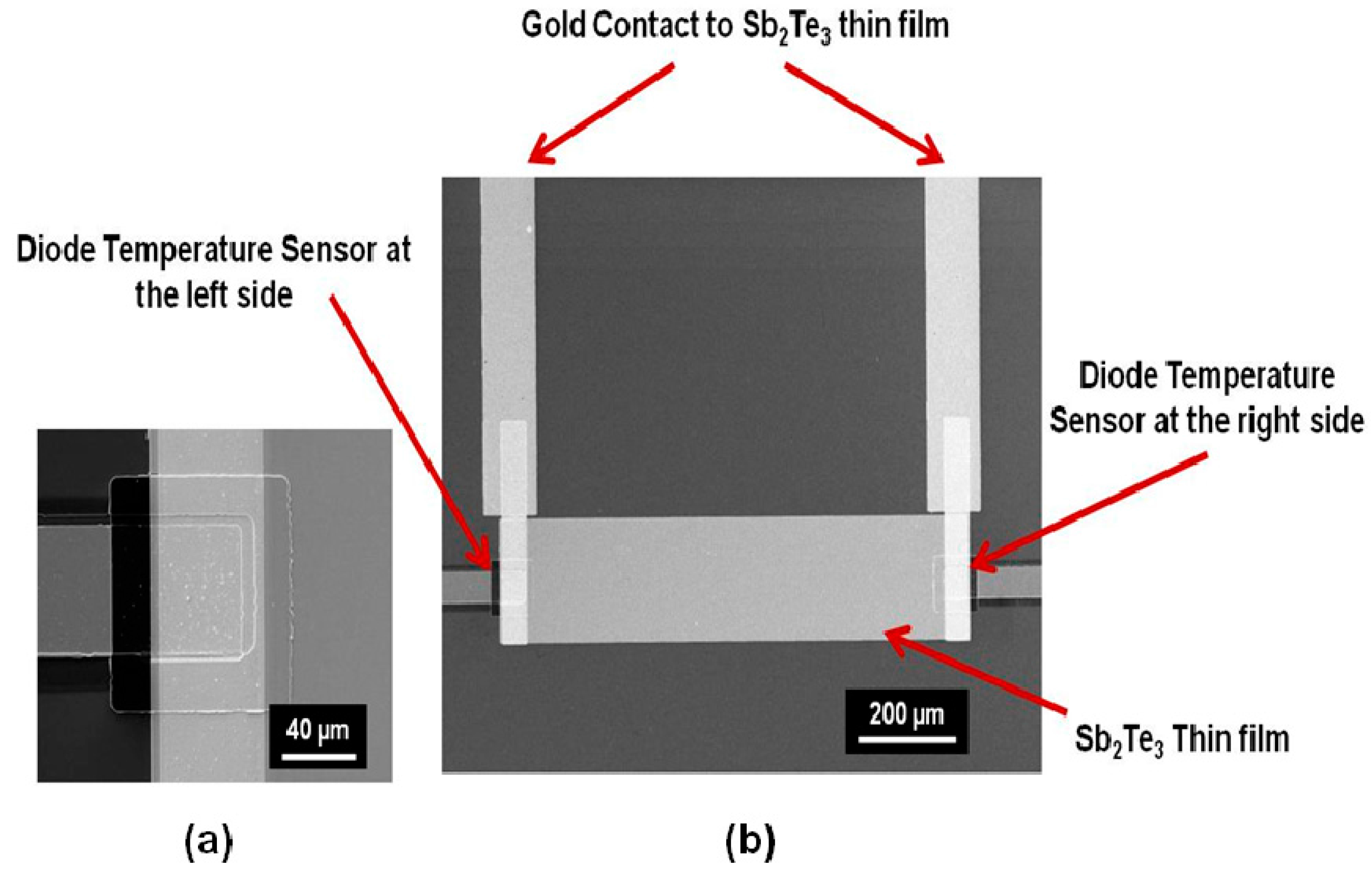
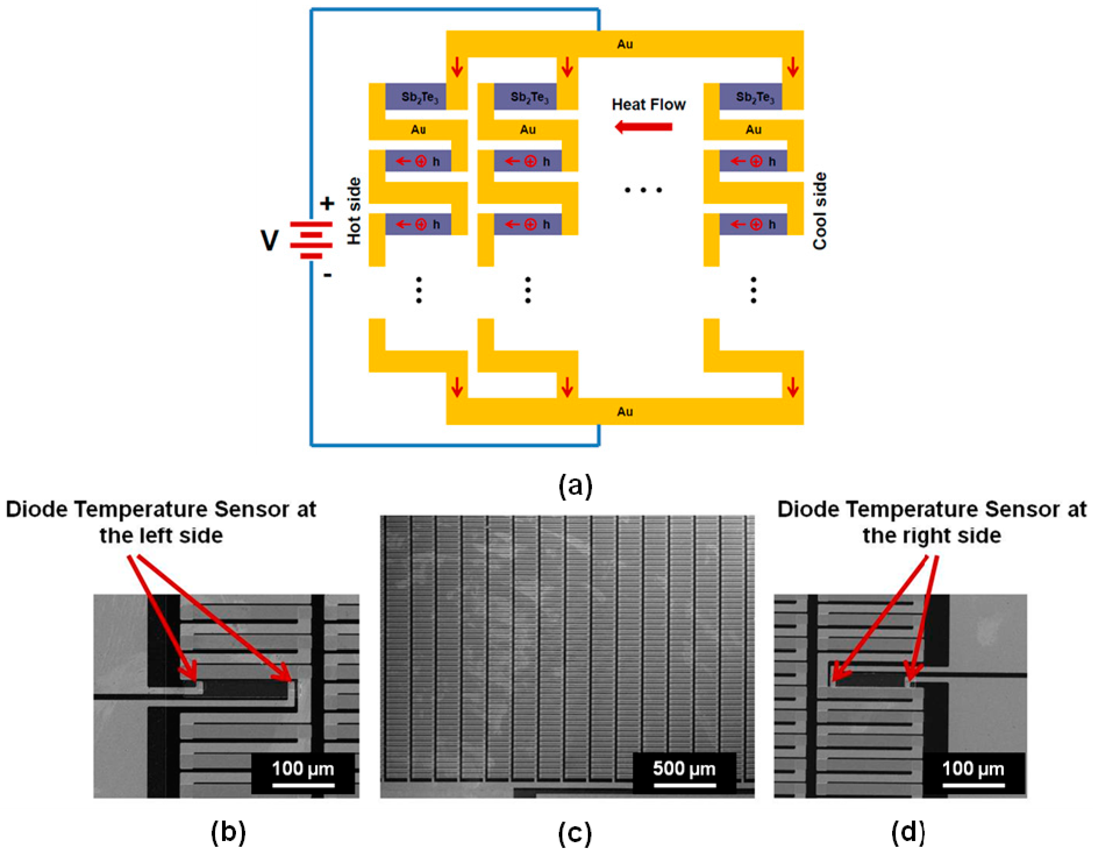
Figure 1a is the schematic of the cross-section of the cross-plane TE device for measuring the cross-plane Seebeck coefficient of the Sb2Te3 thin film, which is sandwiched by a diode temperature sensor and a platinum (Pt) temperature sensor; Figure 1b shows the SEM image of the fabricated cross-plane TE device. The silicon diode temperature sensor centered on the bottom, and the platinum (Pt) serpentine resistor temperature sensor centered on the top. The fabricated cross-plane TE device with pads for the outside contacts has a dimension of 0.7 cm × 0.7 cm, where the active area covered by the Sb2Te3 film is 200 µm × 200 µm. Figure 2 shows the SEM images of the fabricated in-plane TE device and the diode temperature sensor for measuring the in-plane Seebeck coefficient of the Sb2Te3 thin film. Two silicon diode temperature sensors were fabricated at the two ends of the film. The fabricated in-plane TE device with pads for the outside contacts has a dimension of 1 cm × 0.6 cm, where the active area covered by the Sb2Te3 film is 1000 µm × 200 µm. Figure 3a is the working principle for an in-plane integrated TE device of Sb2Te3 thin film; Figure 3b shows the SEM image of an enlarged view on the area of left diode temperature sensors in the integrated TE device; Figure 3c shows the SEM image of a partial of the fabricated integrated TE device; Figure 3d shows the SEM image of an enlarge view on the area of right diode temperature sensors in the integrated TE device. The two silicon diode temperatures were fabricated at the two sides of the device for measuring the temperature difference. The fabricated integrated TE device with pads for the outside contacts has a dimension of 2.5 cm × 2 cm, where the active area covered by the Sb2Te3 elements is 1.5 cm × 1 cm. Sb2Te3 is the thermoelectric material in the device and has the major thermoelectric effect for the device. Gold (Au) is not a thermoelectric material and does not have the thermoelectric effect. The gold layer is the contact material in the device, and can contribute to make a higher ZT value for the device by decreasing the contact resistance with the Sb2Te3 layer. The gold layer does not make any contribution to the Seebeck coefficient.
Figure 1.
(a) Schematic of the cross-section of a cross-plane TE device for measurement of the cross-plane Seebeck coefficient of Sb2Te3 thin film; (b) SEM image of the fabricated TE device.
Figure 1.
(a) Schematic of the cross-section of a cross-plane TE device for measurement of the cross-plane Seebeck coefficient of Sb2Te3 thin film; (b) SEM image of the fabricated TE device.

Figure 2.
(a) SEM image of an enlarged view on a diode temperature sensor; (b) SEM image of a fabricated TE device for measurement of the in-plane Seebeck coefficient of Sb2Te3 thin film, where two diode temperature sensors were fabricated under the two ends of the Sb2Te3 film and separated by an insulation layer of SiO2.

Figure 3.
(a) Working principle for an in-plane integrated TE device of Sb2Te3 thin film; (b) SEM image of an enlarge view on the area of left diode temperature sensors in the integrated TE device; (c) SEM image of a partial of the fabricated integrated TE device; (d) SEM image of an enlarge view on the area of right diode temperature sensors in the integrated TE device.

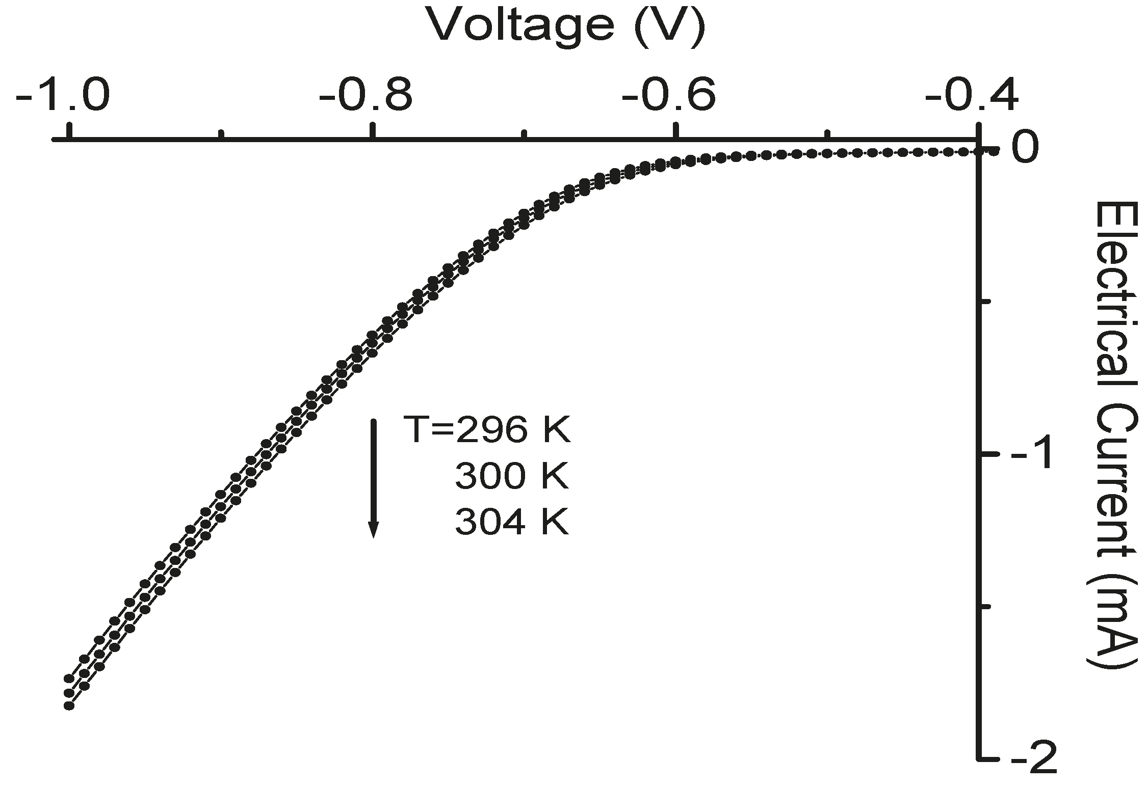
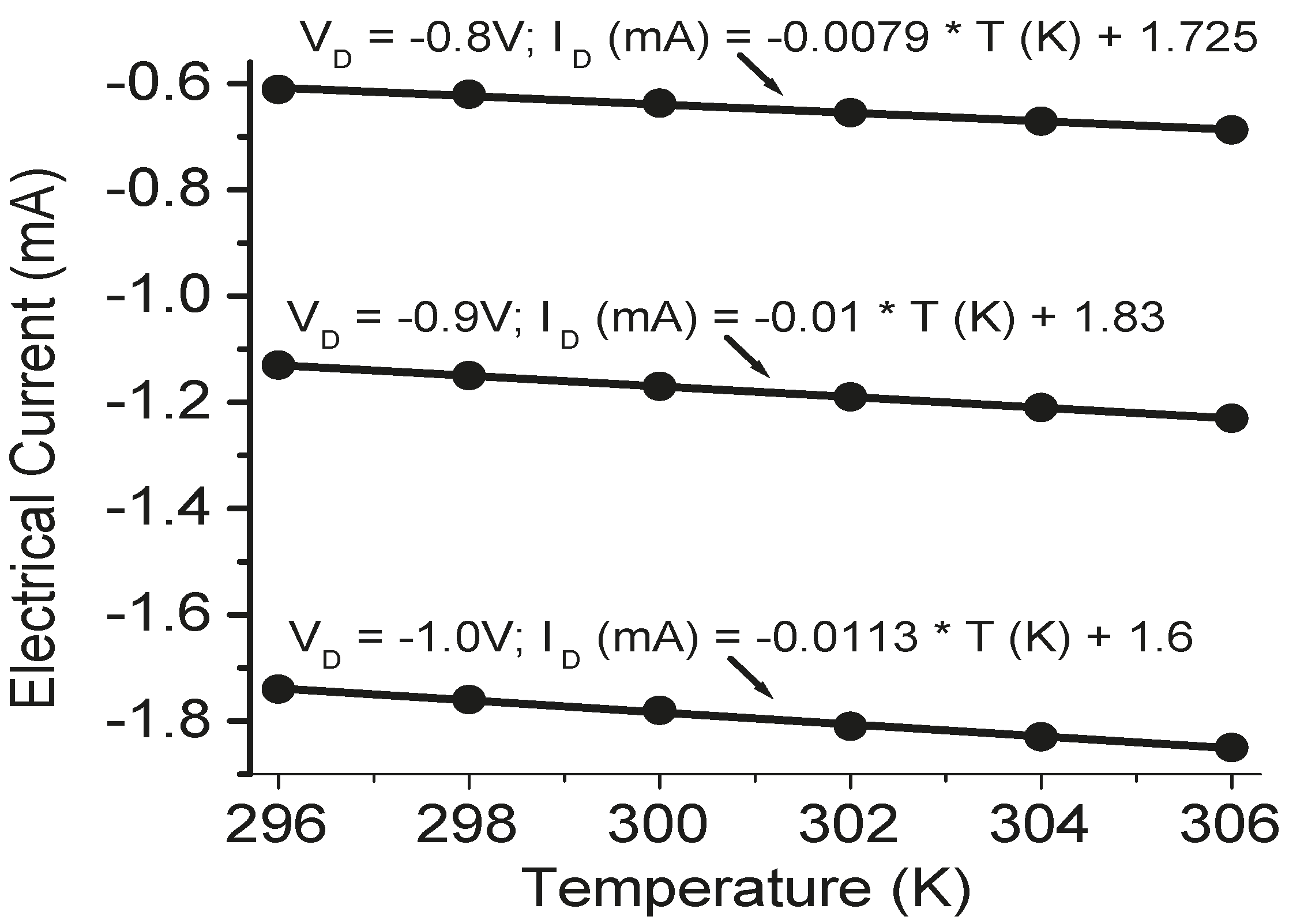
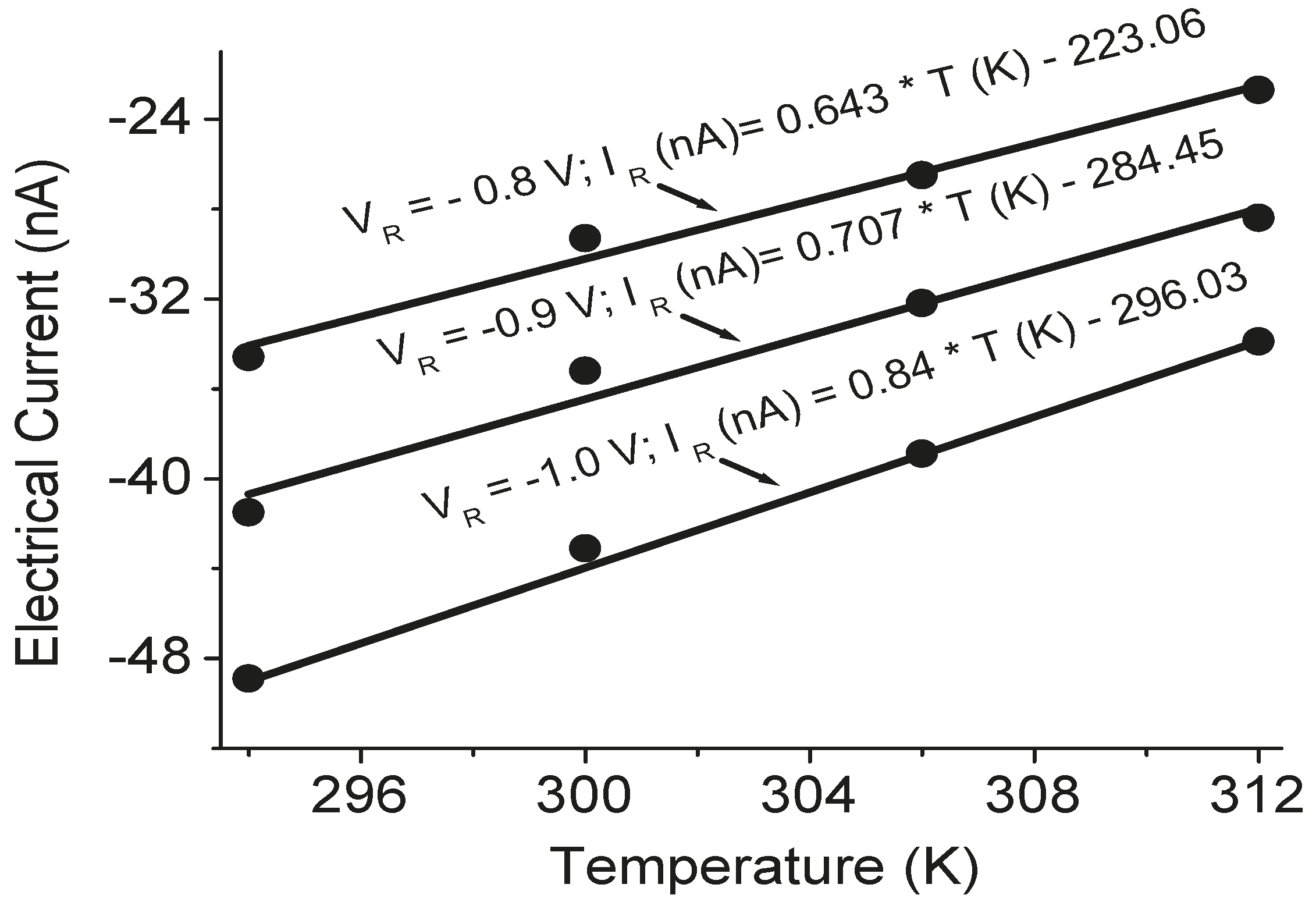
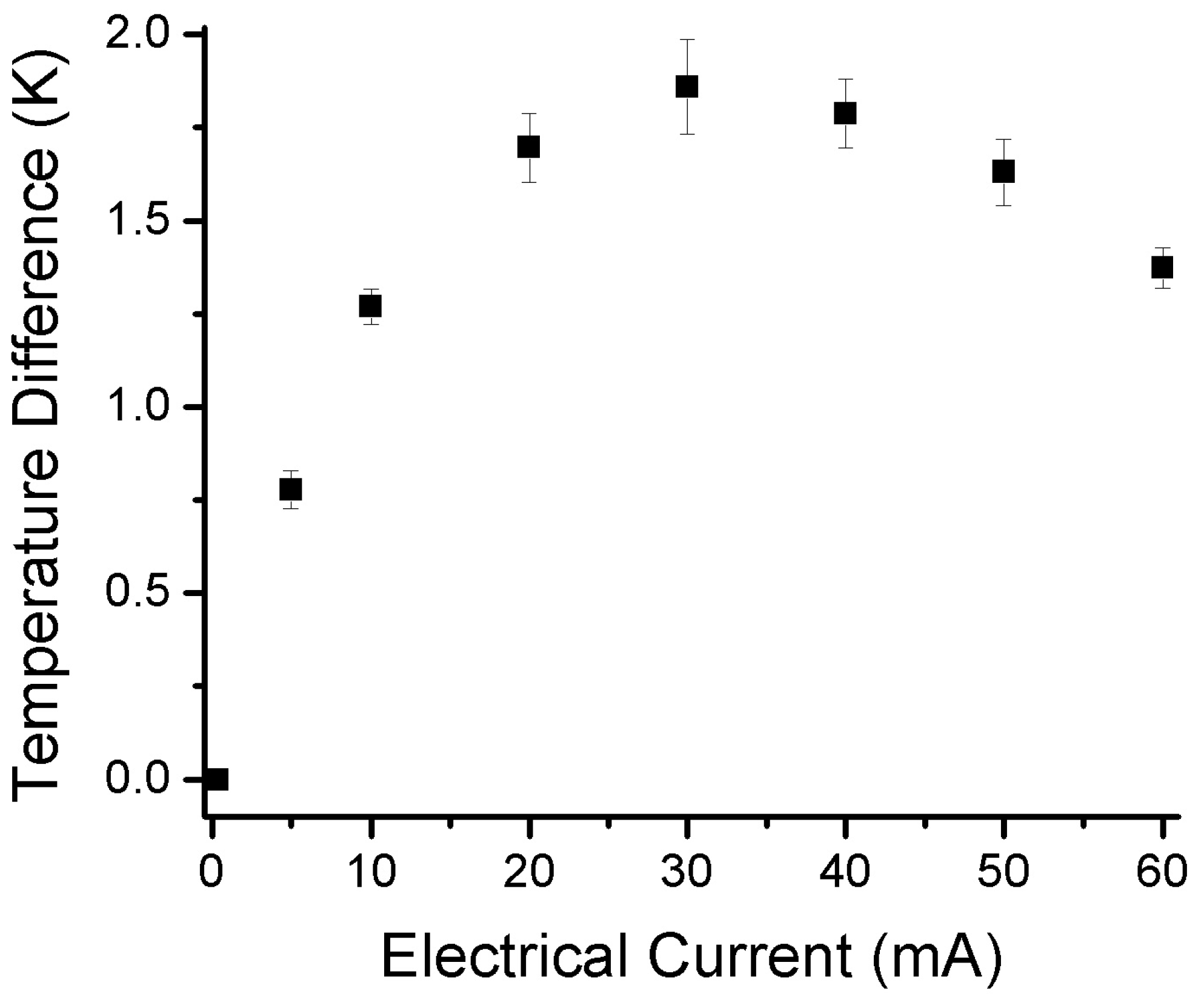
The temperature sensors in the TE devices were calibrated before measurement. The calibration results are shown in Figure 4, Figure 5 and Figure 6. A good linear relation between the electrical current value and temperature was obtained for both Pt serpentine resistor temperature sensor and the silicon diode temperature sensor. The electrical current-voltage (IV) curves in Figure 4 shows the silicon diode temperature sensor has a turn-on voltage of about 0.6 V. The Seebeck coefficient of the Sb2Te3 thin film was then measured, and the measured cross-plane and in-plane Seebeck coefficients were (98 ± 4.5) µV/K and (105.3 ± 5.1) µV/K, respectively. The temperature difference between the left side and the right side of the integrated TE device was measured from the two silicon diode temperature sensors in the device. Figure 7 shows the temperature difference as a function of applied DC electrical currents. The temperature difference increases to a maximum value of about 1.8 K at an applied DC current of 30 mA with the increase of electrical currents, then decreases with further increase of the currents. When the applied current increases, the heating effect becomes larger and larger. As a result, the temperature difference decreases with further increasing current after it reaches its peak value. The ZT value of the integrated Sb2Te3 thin film TE device was obtained as 0.12 ± 0.01. It is possible to make the device to go beyond 1.75 K of temperature difference. The material efficiency of the E-beam-grown Sb2Te3 thin film can be improved by thermal annealing and varying the film thickness for better phonon blocking and hole transmitting in the material, while the efficiency of the device can be further improved by improving the device fabrication such as decreasing the contact resistance.
Figure 4.
The variation of electrical currents as a function of applied voltages at three temperatures (T = 296 K, 300 K, and 304 K) for a fabricated silicon diode temperature sensor.
Figure 4.
The variation of electrical currents as a function of applied voltages at three temperatures (T = 296 K, 300 K, and 304 K) for a fabricated silicon diode temperature sensor.

Figure 5.
The variation of electrical currents as a function of temperatures at three applied voltages (VR = −0.8 V, −0.9 V, and −1.0 V) for a fabricated silicon diode temperature sensor, where the dots are the experimental data, and the linear current-temperature functions were derived from the regression analysis of the experimental data.

Figure 6.
The variation of electrical currents as a function of temperatures at three applied voltage values (VR = −0.8 V, −0.9 V, and −1.0 V) for the platinum resistor temperature sensor in the TE device, where the dots are the experimental data and the linear current-temperature functions were derived from the regression analysis of the experimental data.

Figure 7.
The variation of the temperature difference between the left and right sides of the in-plane Sb2Te3 integrated thermoelectric device as a function of applied DC electrical currents.
Figure 7.
The variation of the temperature difference between the left and right sides of the in-plane Sb2Te3 integrated thermoelectric device as a function of applied DC electrical currents.

4. Conclusions
The silicon diode temperature sensors and thermoelectric devices of Sb2Te3 thin film were fabricated successfully using microfabrication techniques. The electrical property of the fabricated silicon diode temperature sensor versus temperatures was characterized, showing that the diode temperature sensor is highly sensitive to the variation of temperatures. The Seebeck coefficient of Sb2Te3 and the figure merit of the integrated Sb2Te3 thin-film TE device were precisely measured from the devices. The fabrication of silicon diode temperature sensor and thermoelectric thin-film devices are compatible with the integrated circuit (IC) fabrication, and can be used for the applications of on-chip temperature monitoring, surface temperature stabilizing, and more.
Acknowledgments
Research was carried out in part at the Center for Functional Nanomaterials, Brookhaven National Laboratory, which is supported by the US Department of Energy, Office of Basic Energy Sciences, under Contract No. DE-SC00112704; the research is supported by National Science Foundation under Grant No. ECCS-1229312 and EPS-0814103.
Author Contributions
Xiao and Zhu designed the devices and the experiments; Xiao performed the fabrication of the devices and the measurements. Xiao and Zhu analyzed the experimental data and wrote the manuscript.
Conflicts of Interest
The authors declare no conflict of interest.
References
- Han, I.Y.; Kim, S.J. Diode temperature sensor array for measuring micro-scale surface temperatures with high resolution. Sens. Actuators A Phys. 2008, 141, 52–58. [Google Scholar] [CrossRef]
- Chung, D.Y.; Hogan, T.; Brazis, P.; Rocci-Lane, M.; Kannewurf, C.; Bastea, M.; Uher, C.; Kanatzidis, M.G. CsBi4Te6: A high-performance thermoelectric material for low-temperature applications. Science 2000, 287, 1024–1027. [Google Scholar] [CrossRef] [PubMed]
- Yeo, H.K.; Khajetoorians, A.A.; Shi, L.; Pine, K.P.; Ram, R.J.; Shakouri, A.; Shih, C.K. Profiling the thermoelectric power of semiconductor junctions with nanometer resolution. Science 2004, 303, 816–818. [Google Scholar]
- Disalvo, F.J. Thermoelectric cooling and power generation. Science 1999, 285, 703–706. [Google Scholar] [CrossRef] [PubMed]
- Sales, B.C. Smaller is cooler. Science 2002, 295, 1248–1249. [Google Scholar] [CrossRef] [PubMed]
- Tritt, T.M. Holey and unholey semiconductors. Science 1999, 283, 804–805. [Google Scholar] [CrossRef]
- Hsu, K.F.; Loo, S.; Guo, F.; Chen, W.; Dyck, J.S.; Uher, C.; Hogan, T.; Polychronicdis, E.K.; Kanatzidis, M.G. Cubic AgPbmSbTe2+m bulk thermoelectric materials with high figure of merit. Science 2004, 303, 818–820. [Google Scholar] [CrossRef] [PubMed]
- Da Silva, L.W.; Kaviary, M. Micro-thermoelectric cooler interfacial effects on thermal and electrical transport. Int. J. Heat Mass Transf. 2004, 47, 2417–2435. [Google Scholar] [CrossRef]
- Chen, G.; Neagu, M. Thermal conductivity and heat transfer in superlattices. Appl. Phys. Lett. 1997, 71, 2761–2763. [Google Scholar] [CrossRef]
- Chen, G.; Shakouri, A. Heat transfer in nanostructures for solid-state energy conversion. J. Heat Transf. 2002, 124, 242–252. [Google Scholar] [CrossRef]
- Cahill, D.G.; Ford, W.K.; Goodson, K.E.; Mahan, G.D.; Majumdar, A.; Maris, H.J.; Merlin, R.; Phillpot, S.R. Nanoscale thermal transport. J. Appl. Phys. 2003, 93, 793–818. [Google Scholar] [CrossRef]
- Majumdar, A. Thermoelectricity in semiconductor nanostructures. Science 2004, 303, 777–778. [Google Scholar] [CrossRef] [PubMed]
- Hicks, L.D.; Harmon, T.C.; Sun, X.; Dresselhaus, M.S. Experimental study of the effect of quantum well structures on the thermoelectric figure of merit. Phys. Rev. B Rapid 1996, 53, R10493–R10496. [Google Scholar] [CrossRef]
- Venkatasubramanian, T.; Colpitts, T.; El-Masry, N.; Lamvik, M. MOCVD of Bi2Te3, Sb2Te3 and their superlattice structures for thin-film thermoelectric applications. J. Cryst. Growth 1997, 170, 817–821. [Google Scholar] [CrossRef]
- Xiao, Z.; Hedgemen, K.; Harrison, M.; DiMasi, E. Fabrication of Bi2Te3/Sb2Te3 and Bi2Te3/Bi2Te2Se multilayered thin film-based integrated cooling devices. J. Vac. Sci. Technol. A 2010, 28, 679–683. [Google Scholar] [CrossRef]
- Hines, M.; Lenhardt, M.; Lu, M.; Jiang, L.; Xiao, Z. Cooling effect of nanoscale Bi2Te3/Sb2Te3 multilayered thermoelectric thin films. J. Vac. Sci. Technol. A 2012, 30. [Google Scholar] [CrossRef]
- Venkatasubramanian, R.; Siilvola, E.; Colpitts, T.; O’Quinn, B. Thin-film thermoelectric devices with high room-temperature figures of merit. Nature 2001, 413, 597–602. [Google Scholar] [CrossRef] [PubMed]
- Xiao, Z.; Zimmerman, R.L.; Holland, L.R.; Zheng, B.; Muntele, C.I.; Ila, D. Nanoscale BixTe3/Sb2Te3 multilayer thin film materials for reduced thermal conductivity. Nucl. Instrum. Methods Phys. Res. Sect. B 2006, 242, 201–204. [Google Scholar] [CrossRef]
© 2015 by the authors; licensee MDPI, Basel, Switzerland. This article is an open access article distributed under the terms and conditions of the Creative Commons Attribution license (http://creativecommons.org/licenses/by/4.0/).
Share and Cite
MDPI and ACS Style
Xiao, Z.; Zhu, X. On-Chip Sensing of Thermoelectric Thin Film’s Merit. Sensors 2015, 15, 17232-17240. https://doi.org/10.3390/s150717232
AMA Style
Xiao Z, Zhu X. On-Chip Sensing of Thermoelectric Thin Film’s Merit. Sensors. 2015; 15(7):17232-17240. https://doi.org/10.3390/s150717232
Chicago/Turabian StyleXiao, Zhigang, and Xiaoshan Zhu. 2015. "On-Chip Sensing of Thermoelectric Thin Film’s Merit" Sensors 15, no. 7: 17232-17240. https://doi.org/10.3390/s150717232