
Detection Wavelength Control of Uncooled Infrared Sensors Using Two-Dimensional Lattice Plasmonic Absorbers †


Abstract
:1. Introduction
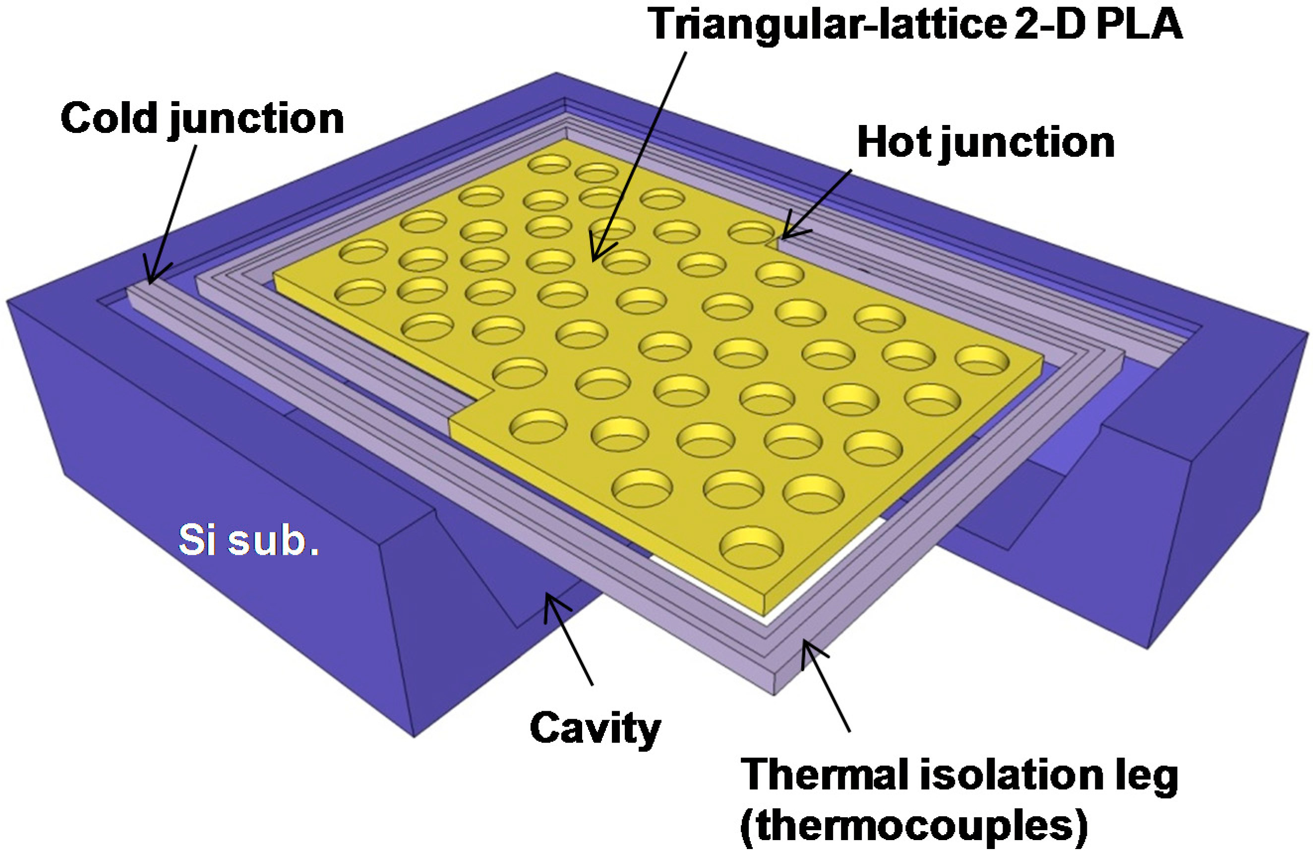
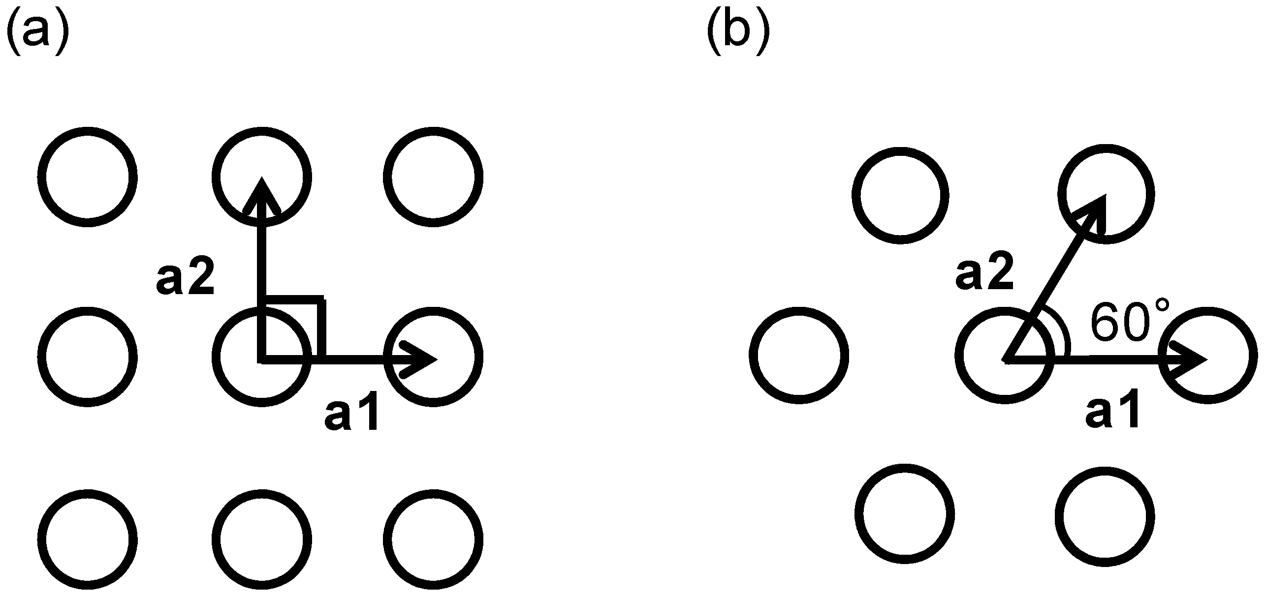
2. Design

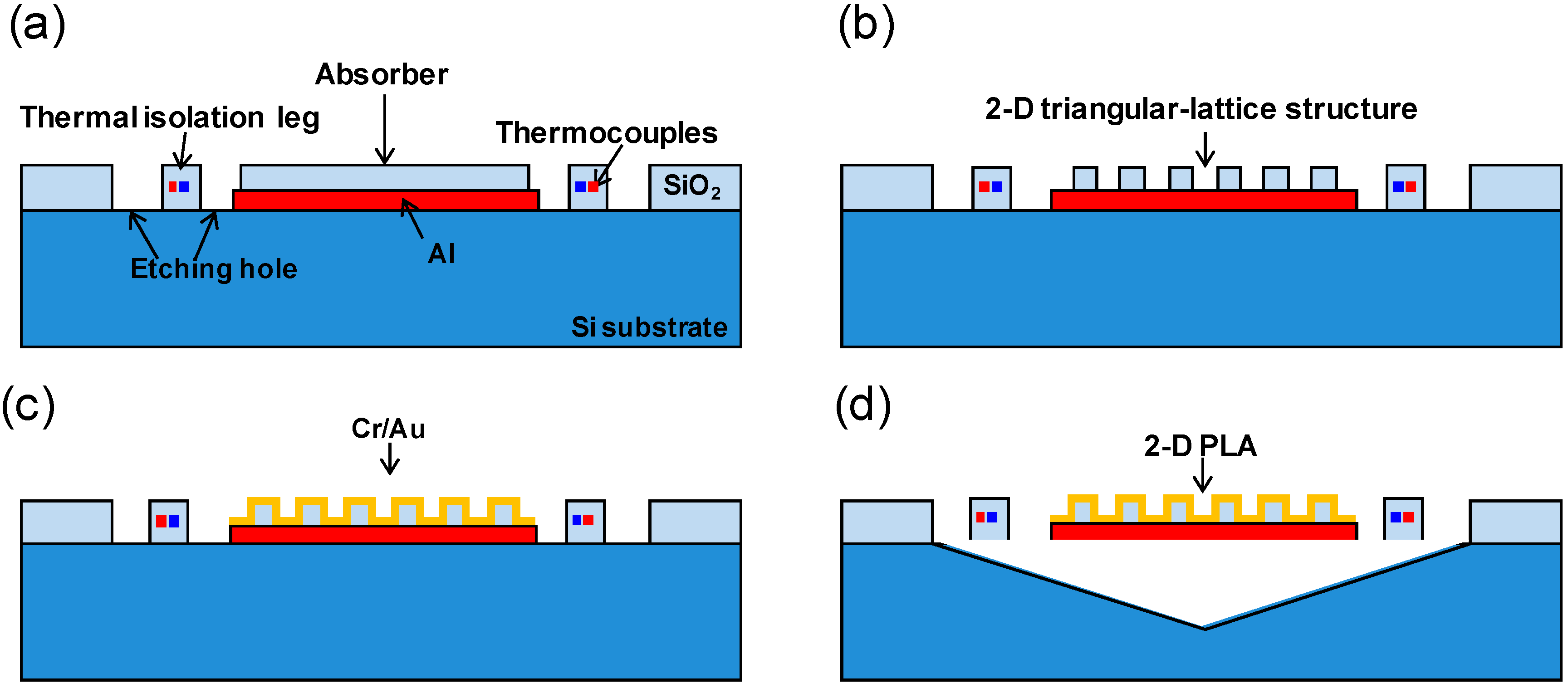
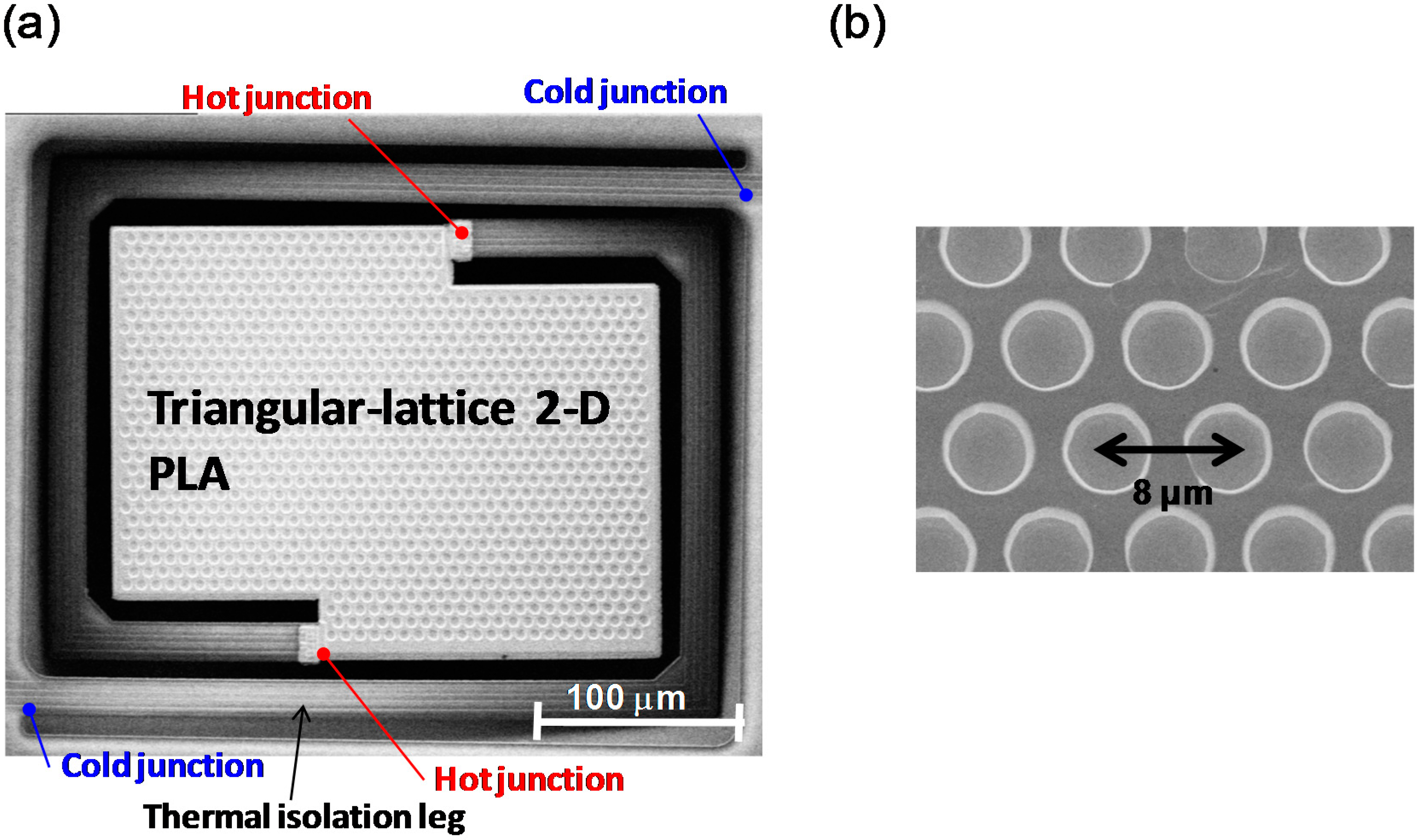
3. Sensor Fabrication

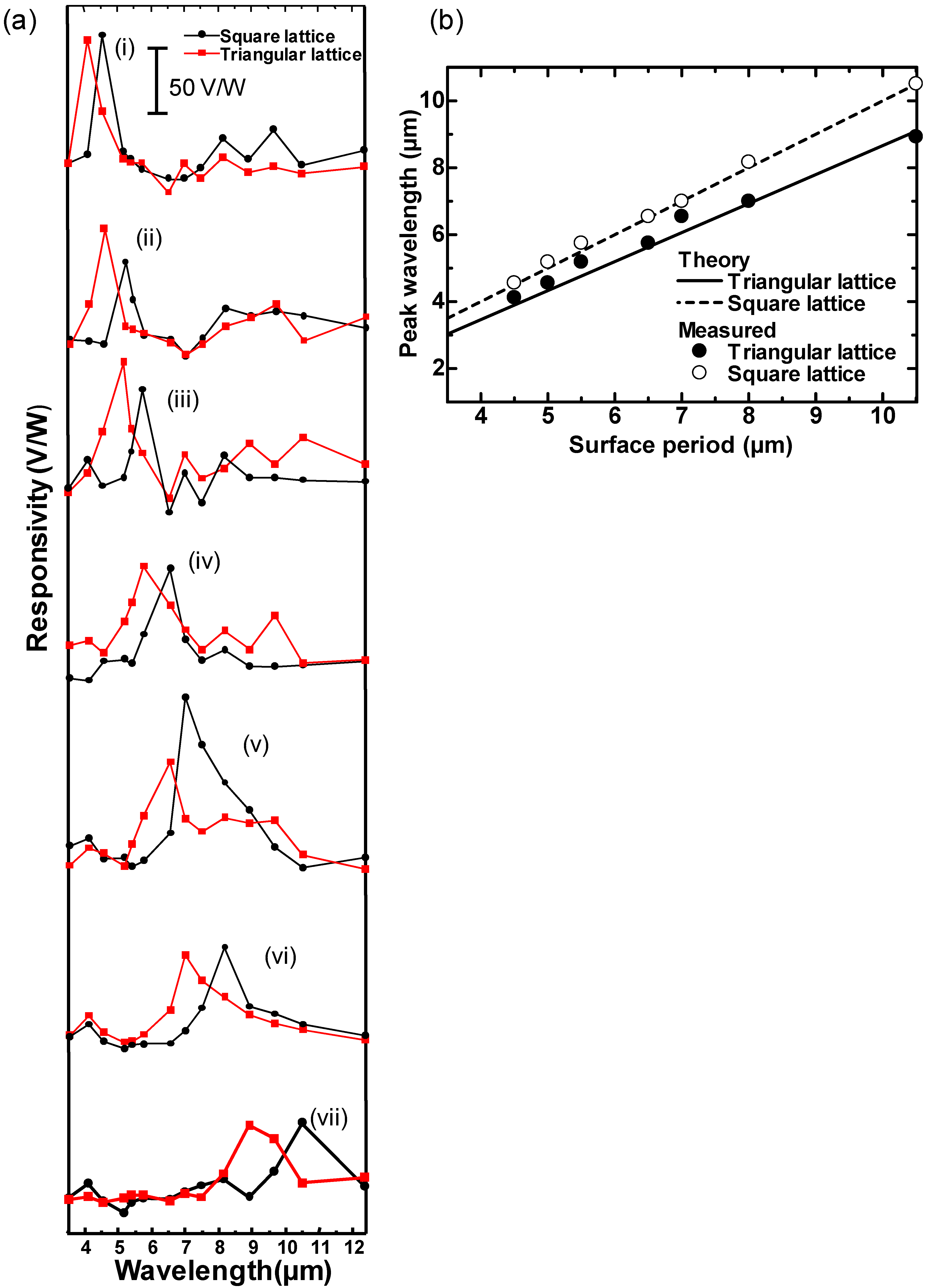
4. Measurements
5. Discussion

6. Conclusions
Acknowledgments
Author Contributions
Conflicts of Interest
References
- Kruse, P.W. Uncooled Thermal Imaging Arrays, Systems, and Applications; SPIE: Washington, DC, USA, 2001; pp. 25–56. [Google Scholar]
- Vollmer, M.; Mollmann, K.-P. Spectrally Resolved Infrared Thermal Imaging. In Infrared Thermal Imaging: Fundamentals, Research and Applications; Wiley-VCH: Weinheim, Germany, 2010; pp. 157–185. [Google Scholar]
- Kimata, M. Trends in small-format infrared array sensors. In Proceedings of the Sensors, Baltimore, MD, USA, 3–6 November 2013; pp. 1–4.
- Ozbay, E. Plasmonics: Merging photonics and electronics at nanoscale dimensions. Science 2006, 311, 189–193. [Google Scholar] [CrossRef] [PubMed]
- Stanley, R. Plasmonics in the mid-infrared. Nat. Photon. 2012, 6, 409–411. [Google Scholar] [CrossRef]
- Kawata, S. Plasmonics: Future Outlook. Jpn. J. Appl. Phys. 2013, 52. [Google Scholar] [CrossRef]
- Smith, D.R.; Pendry, J.B.; Wiltshire, M.C. Metamaterials and negative refractive index. Science 2004, 305, 788–792. [Google Scholar] [CrossRef] [PubMed]
- Pendry, J.B.; Martin-Moreno, L.; Garcia-Vidal, F.J. Mimicking surface plasmons with structured surfaces. Science 2004, 305, 847–848. [Google Scholar] [CrossRef] [PubMed]
- Tanaka, T. Plasmonic metamaterials. IEICE Elec. Exp. 2012, 9, 34–50. [Google Scholar] [CrossRef]
- Talghader, J.J.; Gawarikar, A.S.; Shea, R.P. Spectral selectivity in infrared thermal detection. Light Sci. Appl. 2012, 1. [Google Scholar] [CrossRef]
- HaïDar, R.; Vincent, G.; Collin, S.; Bardou, N.; GuéRineau, N.; Deschamps, J.; Pelouard, J.-L. Free-standing subwavelength metallic gratings for snapshot multispectral imaging. Appl. Phys. Lett. 2010, 96, 221104. [Google Scholar] [CrossRef]
- Ohtera, Y.; Yamada, H. Photonic crystals for the application to spectrometers and wavelength filters. IEICE Elec. Exp. 2013, 10, 20132001. [Google Scholar] [CrossRef]
- Wang, Y.; Potter, B.J.; Talghader, J.J. Coupled absorption filters for thermal detectors. Opt. Lett. 2006, 31, 1945–1947. [Google Scholar] [CrossRef] [PubMed]
- Han, S.W.; Kim, J.W.; Sohn, Y.S.; Neikirk, D.P. Design of infrared wavelength-selective microbolometers using planar multimode detectors. Elec. Lett. 2004, 40, 1410–1411. [Google Scholar] [CrossRef]
- Maier, T.; Brueckl, H. Multispectral microbolometers for the mid-infrared. Opt. Lett. 2010, 35, 3766–3768. [Google Scholar] [CrossRef] [PubMed]
- Ogawa, S.; Okada, K.; Fukushima, N.; Kimata, M. Wavelength selective uncooled infrared sensor by plasmonics. Appl. Phys. Lett. 2012, 100, 021111. [Google Scholar] [CrossRef]
- Ogawa, S.; Komoda, J.; Masuda, K.; Kimata, M. Wavelength selective wideband uncooled infrared sensor using a two-dimensional plasmonic absorber. Opt. Eng. 2013, 52. [Google Scholar] [CrossRef]
- Ogawa, S.; Masuda, K.; Takagawa, Y.; Kimata, M. Polarization-selective uncooled infrared sensor with asymmetric two-dimensional plasmonic absorber. Opt. Eng. 2014, 53. [Google Scholar] [CrossRef]
- Ogawa, S.; Fujisawa, D.; Maegawa, T.; Ueno, M.; Kimata, M. Three-Dimensional Plasmonic Metamaterial Absorbers for High-Performance Wavelength Selective Uncooled Infrared Sensors. In Proceedings of Infrared Technology and Applications XL, Baltimore, MD, USA, 5 May 2014.
- Fujisawa, D.; Ogawa, S.; Hata, H.; Uetsuki, M.; Misaki, K.; Takagawa, Y.; Kimata, M. Multi-color imaging with silicon-on-insulator diode uncooled infrared focal plane array using through-hole plasmonic metamaterial absorbers. In Proceedings of the 28th IEEE International Conference on Micro Electro Mechanical Systems (MEMS), Estoril, Portugal, 18–22 January 2015; pp. 905–908.
- Ogawa, S.; Fujisawa, D.; Hata, H.; Uetsuki, M.; Misaki, K.; Kimata, M. Mushroom plasmonic metamaterial infrared absorbers. Appl. Phys. Lett. 2015, 106, 041105. [Google Scholar] [CrossRef]
- Ogawa, S.; Komoda, J.; Masuda, K.; Takagawa, Y.; Kimata, M. Wavelength selective uncooled infrared sensor using triangular-lattice plasmonic absorbers. In Proceedings of the 2013 International Conference on Optical MEMS and Nanophotonics (OMN), Kanazawa, Japan, 18–22 August 2013; pp. 61–62.
- Maier, S.A. Plasmonics: Fundamentals and Applications; Springer: New York, NY, USA; p. 146.
- Balin, I.; Dahan, N.; Kleiner, V.; Hasman, E. Slow surface phonon polaritons for sensing in the midinfrared spectrum. Appl. Phys. Lett. 2009, 94, 111112. [Google Scholar] [CrossRef]
- Vollmer, M.; Mollmann, K.-P. Thermoelectric Effects. In Infrared Thermal Imaging: Fundamentals, Research and Applications; Wiley-VCH: Weinheim, Germany, 2010; pp. 310–311. [Google Scholar]
- Masuda, K.; Ogawa, S.; Takagawa, Y.; Kimata, M. Optimization of two-dimensional plasmonic absorbers based on a metamaterial and cylindrical cavity model approach for high-responsivity wavelength-selective uncooled infrared sensors. Sens. Mater. 2014, 26, 215–223. [Google Scholar]
- Miroshnichenko, A.E.; Flach, S.; Kivshar, Y.S. Fano resonances in nanoscale structures. Rev. Mod. Phys. 2010, 82, 2257–2298. [Google Scholar] [CrossRef]
- Fujisawa, D.; Maegawa, T.; Ohta, Y.; Kosasayama, Y.; Ohnakado, T.; Hata, H.; Ueno, M.; Ohji, H.; Sato, R.; Katayama, H.; et al. Two-million-pixel SOI diode uncooled IRFPA with 15 μm pixel pitch. In Proceedings of the Infrared Technology and Applications XXXVIII, Baltimore, MA, USA, 23 April 2012.
- Maegawa, T.; Fujisawa, D.; Hata, H.; Ogawa, S.; Ueno, M. 2-in-1 diodes with a contact-sidewall structure for small pixel pitch in silicon-on-insulator (SOI) uncooled infrared (IR) focal plane arrays. Sens. Mater. 2014, 26, 229–238. [Google Scholar]
© 2015 by the authors; licensee MDPI, Basel, Switzerland. This article is an open access article distributed under the terms and conditions of the Creative Commons Attribution license (http://creativecommons.org/licenses/by/4.0/).
Share and Cite
Takagawa, Y.; Ogawa, S.; Kimata, M. Detection Wavelength Control of Uncooled Infrared Sensors Using Two-Dimensional Lattice Plasmonic Absorbers. Sensors 2015, 15, 13660-13669. https://doi.org/10.3390/s150613660
Takagawa Y, Ogawa S, Kimata M. Detection Wavelength Control of Uncooled Infrared Sensors Using Two-Dimensional Lattice Plasmonic Absorbers. Sensors. 2015; 15(6):13660-13669. https://doi.org/10.3390/s150613660
Chicago/Turabian StyleTakagawa, Yousuke, Shinpei Ogawa, and Masafumi Kimata. 2015. "Detection Wavelength Control of Uncooled Infrared Sensors Using Two-Dimensional Lattice Plasmonic Absorbers" Sensors 15, no. 6: 13660-13669. https://doi.org/10.3390/s150613660