3. Results and Discussion
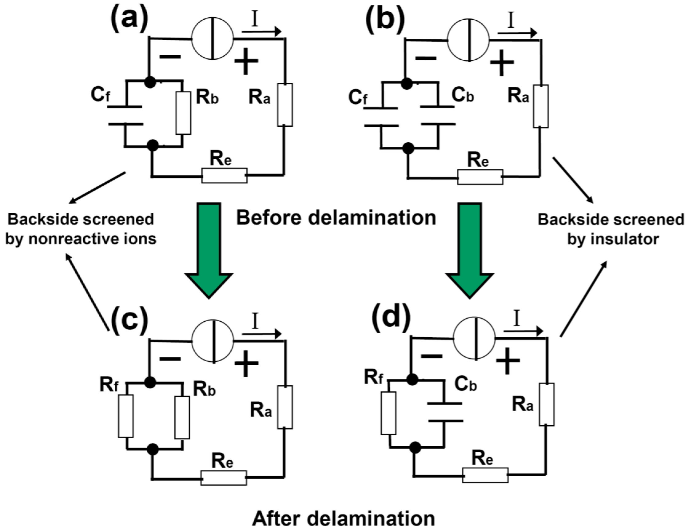
In order to quantitatively understand the delamination process, we develop a capacitor model as shown in
Figure 2. In
Figure 2a,c, the front side of the Pt cathode is covered by spin-coated PMMA and the backside is open (sample type A).
Figure 2a,c describes the case before and after the delamination, respectively. R
a and R
e are resistances associated with the anode and electrolytic solution. At the cathode, the
interface resistance between the Pt backside and the solution is represented by R
b. The front side can be regarded as a capacitor C
f, formed between the Pt bulk and the electrolytic solution with the dielectric being the PMMA, see also
Figure 1a. Note that the insulation resistance for capacitor C
f is not infinite because there is a path for leakage current at the Pt edge, but we will ignore this effect for simplicity. Also, the resistance of the bulk Pt is neglected. A constant current I is applied to the electrolysis cell (
Figure 2a). As long as IR
b is greater than the critical breakdown voltage V
f0 of the capacitor C
f, the PMMA starts to peel off. In the end of the delamination, the front surface of the Pt is entirely open and the
interface resistance to the solution is denoted by R
f (
Figure 2c). Therefore, the bubbling separation process can be conveniently described by this lumped circuit model. Note that the breakdown of C
f does not occur across the dielectric, but rather along the PMMA. The PMMA-Pt interface is much easier to break down (
i.e., delamination) compared to the electric puncture of the PMMA itself.
Figure 2b,d illustrates a similar situation as
Figure 2a,c, but the open surface of the backside Pt is now covered with a thick and inflexible PMMA block (
Figure 1b, sample type B). In this case, both sides are modeled by capacitors (C
f and C
b). With the voltage increasing, the bubbles attack C
f first, leading to the (interface) breakdown of the capacitor. After delamination, R
f is used to describe the Pt-solution interface resistance, whereas C
b which is very difficult to break down remains basically unchanged.
Figure 2.
Capacitor model of the electrochemical delamination of 2D materials. (a,b) are before while (c,d) are after the delamination. The delamination is modeled by the Cf (formed between the solution and substrate) breakdown into Rf, which is boosted by two types of screening effects from nonreactive ions and stable insulator at the backside of substrate.
Clearly, the efficiency for delamination is determined by how fast the breakdown of C
f takes place. Now we will experimentally demonstrate that a screening effect on the backside Pt open surface can greatly boost the delamination of the front side thin PMMA by accelerating the speed to reach the critical breakdown voltage of C
f. This screening effect can be induced by: (1) large numbers of non-reactive ions, e.g., Na
+, surrounding the Pt backside as a “cloud” (
Figure 1a), or (2) an insulator such as drop-coated thick PMMA block physically covering the Pt backside (
Figure 1b).
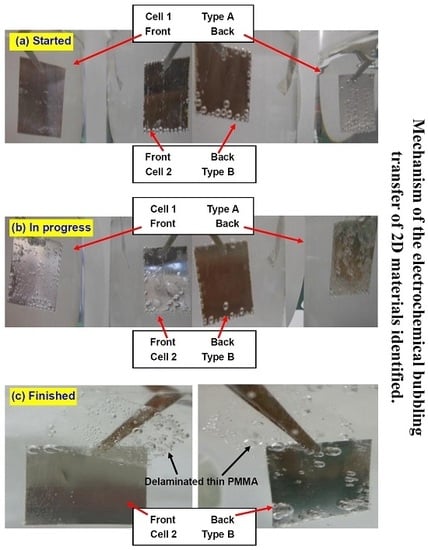
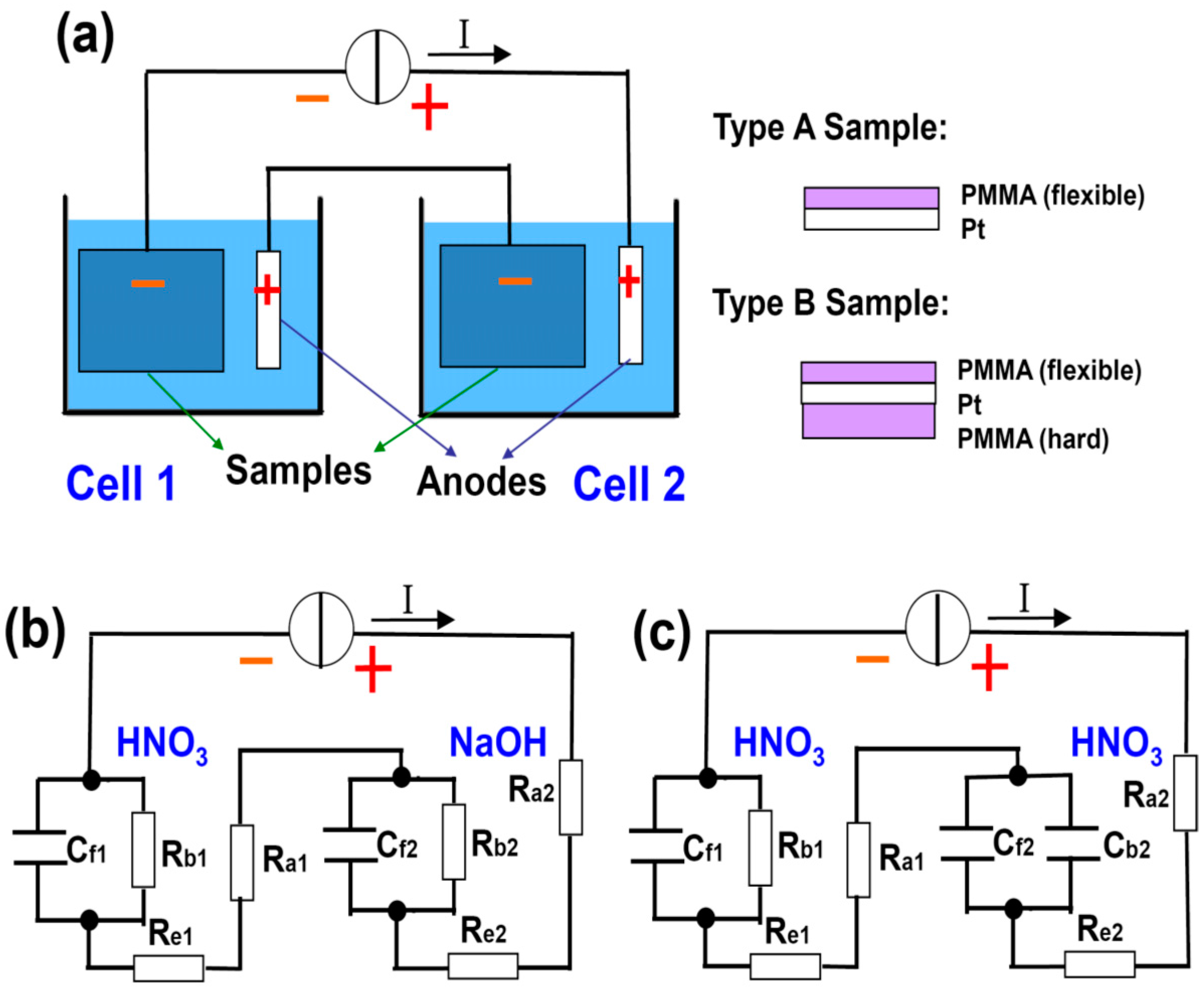
Figure 3a shows the schematic diagram of our setup, where the PMMA delamination time in two water electrolysis cells are compared. They are connected in series to a constant current source to ensure that they have equal currents and hence equal amount of H
2 bubbles generated (assuming 100% current efficiency). This configuration facilitates our experimental observation, allowing the direct comparison of the delamination on site.
Table 1 lists the parameters used, where tests 1 and 2 are designed to examine the screening effects from nonreactive cations and insulator, respectively. HNO
3 and NaOH are used as the electrolytes. A monobasic acid (e.g., HNO
3) is chosen instead of polybasic acid (e.g., H
2SO
4) because at the same concentration it releases an equal amount of cations as NaOH, which is a monobasic base. The concentration and volume of the solutions are fixed at 0.25 mol/L and 200 mL. A constant current of 0.5 A is applied to the systems. Two types of samples (A and B), as schematically drawn in
Figure 3a, are used as the cathode in the two cells (see
Table 1).
Based on
Figure 2, it can be seen that during the breakdown process of C
f, the total voltage drop across the electrolysis cell (between “+” and “−”) decreases and reaches its minimum when the delamination ends [
13]. Together with direct eye observation, they are used as the criteria to determine the completion of the delamination. The equivalent circuits for tests 1 and 2 are shown in
Figure 3b,c. In test 1, cell 1 contains many H
+ ions primarily generated by the ionization of HNO
3, which can be easily reduced at the uncovered backside of Pt foil. In cell 2, however, the majority cations that contribute to the conductivity are Na
+ from NaOH. Even though they do not participate in the redox reaction, they carry the current and migrate towards the cathode. As a result, the gathering of Na
+ shields the backside of the Pt cathode to some extent, hindering H
+ from being reduced to H atoms by generating a large Coulomb repulsive force. Therefore, many H
+ are forced to squeeze into the interface between PMMA and Pt and accept electrons therein. As the reaction front advances towards the interior, the bubbles eventually separate the two materials. The cloud of Na
+ hence offers a screening effect against H
+ at the Pt back, serving as the driving force for the hydrogen to form a wedge between the partly exfoliated PMMA and free Pt surface, and the subsequent continuous widening of this wedge. When the Na
+ accumulation reaches its steady stage, the freshly arrived Na
+ are neutralized by the OH
− produced by water decomposition 2H
2O + 2e
− = H
2 + 2OH
− and the net Na
+ density is thus stabilized and stops increasing. In
Figure 3b, the difference between the two cells in terms of the screening effect can also be understood as R
b1 << R
b2. At the given current I, the voltage IR
b2 on C
f2 is high enough to trigger the breakdown of C
f2, whereas IR
b1 is too small and hardly reaches the threshold breakdown voltage of C
f1. Indeed, in experiments we observe that it takes approximately 2 min for the PMMA delamination to complete in cell 2, which never happens in cell 1 within 5 min. The role for an appropriate electrolyte is not simply boosting the conductivity of solution, but providing the driving force to bubble off of the PMMA as well.
Figure 3.
(
a) Schematic drawing of the setup for comparison study of two electrochemical cells connected in series so that the amounts of generated bubbles at cathodes are equal. Two types of samples are used in the experiments; (
b,
c) are the equivalent circuits for test 1 and 2, respectively (see
Table 1).
Table 1.
Summary of the electrochemical delamination comparison experiments using H2 bubbles.
Table 1.
Summary of the electrochemical delamination comparison experiments using H2 bubbles.
| | | Electrolysis Cell 1 | Electrolysis Cell 2 | Constant Current (A) |
|---|
| Test 1 | Electrolyte | HNO3 | NaOH | 0.5 |
| (aq. solution, 0.25 mol/L, 200 mL) |
| Sample at cathode | Type A | Type A |
| Test 2 | Electrolyte | HNO3 | HNO3 | 0.5 |
| (aq. solution, 0.25 mol/L, 200 mL) |
| Sample at cathode | Type A | Type B |
With this understanding, we can intentionally design an even more effective screening. In test 2, both solutions are HNO
3, but the sample in cell 2 is changed to type B (
Table 1 and
Figure 3c). The backside of the type B sample is covered with a drop-coated PMMA block. It is inflexible and renders it almost impossible for a wedge to form at its interface to Pt. Therefore, it is supposed to entirely screen out H
+ at the back and force them to be reduced at the interface between the thin/flexible front side PMMA and the Pt. This means R
b2 will be dramatically increased (to infinity ideally) in
Figure 3c, which is denoted by C
b2 instead. Other parameters remain unchanged with respect to test 1.
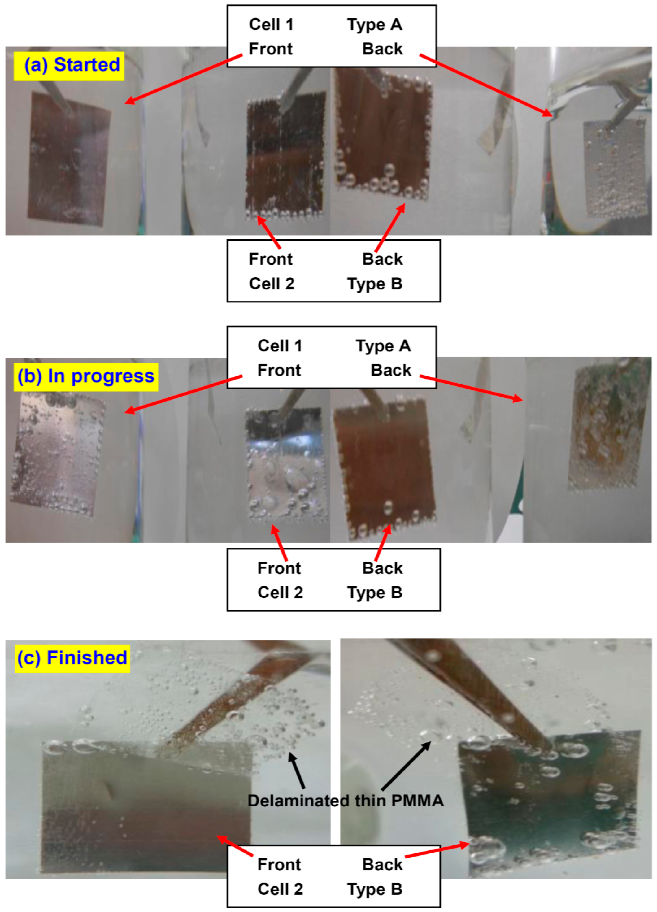
Figure 4 summarizes the photos of the samples taken at different stages. At the early stage of the procedure (5 s after power-on), the bubbles on type A sample in cell 1 dominantly appear on the backside, with the front side free of bubbles (
Figure 4a). On the contrary, for type B sample, the bubbles gather mainly on the front, whereas there are almost no bubbles on the back, except at sample edges. After 2 min of electrolysis, a few bubbles can be seen on the front side of type A sample, but the majority are still on the backside (
Figure 4b). On the other hand, the bubbles on the front side of type B sample already have evolved into large bubbles and the delamination is almost finished; the backside is still clear. Finally, after 5 min, type A sample is almost not exfoliated at all, due to the lack of screening from either passive cations or a stable insulator. In contrast, the PMMA film at the front side of type B sample has long since detached entirely (
Figure 4c). The backside PMMA is very thick and inflexible, generating a good screening effect. This PMMA keeps attaching to the surface.
Figure 4.
Photos of the samples where the experiment is (a) just started; (b) in progress and (c) already finished. The front side thin PMMA layer is entirely peeled off from the type B sample in cell 2 whereas remains undetached on the type A sample in cell 1. It is explained by the screening effect induced by the PMMA block at the backside of type B sample.
The screening theory seems to dovetail well with the experimental findings. Microscopically, however, is the amount of Na+ really enough to create such a screening effect? When there is no current, on the Pt surface in 0.25 mol/L NaOH, the average distance between Na+ ions is estimated to be 1.9 nm. During the electrolysis, if all the Na+ ions in the 0.2 L solution is attracted and condensed on the backside Pt surface (2 cm × 2 cm), is then 0.15 pm. Of course, this calculated extreme case will never happen, but it gives an indication that the total amount of Na+ under our condition is several orders of magnitude more than enough to provide a screening effect against H+. In reality, some limited amount of H2 bubbles can still generate on the backside, unless it is perfectly shielded by an insulator that is stable enough to survive the bubbling delamination process.
Oxygen bubbles can also be used to separate the films, which is also heavily affected by the screening effect. We have done a series of experiments listed in
Table 2. Compared with
Table 1, here all samples are used as the anodes, and in test 4 the electrolytes are changed to NaOH. Other parameters are kept unchanged. Not surprisingly, in test 3, the delamination in HNO
3 is far more efficient than in NaOH. It can be readily explained by the screening effect from the nonreactive NO
3− against OH
− anions which are sources for O
2 generation. In test 4, type B sample works much better than type A sample due to the screening effect from the thick and nonflexible PMMA insulator at the back. Even though the screening theory works perfectly in predicting the experimental results for tests 3 and 4, however, we also notice that tests 1, 2 and tests 3, 4 are not entirely symmetric. In general, to delaminate a thin film, it takes 3–4 times longer time using O
2 bubbles than using H
2 bubbles. We believe the reasons for the deficiency of O
2 bubbles in the exfoliation are three folds. First, the O
2 evolution reaction at the anode is much more complicated and less efficient than the H
2 evolution at the cathode. The exchange current densities for water oxidation on the best known catalysts RuO
2 is 2–3 orders of magnitude lower than that for H
2 production, meaning that these anodes generally operate at high overpotentials [
14]. Also, most transition metals are catalysts for H
2 evolution (can be simplified as H + H = H
2; Pt is the best known catalyst in particular), but not O
2 evolution [
14]. Second, the radii of OH
− is 1.4 Å [
15,
16], several times larger than 0.4 Å of H
+ (here we use Shannon’s “effective ionic radius” values where the hydrated ion enlargement effect is taken into account) [
15]. The considerably greater volume makes it more difficult for OH
− to intercalate into the interface. Also, it is known that protons have an unconventionally high mobility in solutions due to the proton hopping mechanism as well as their low mass, which further enhances the H
+ intercalation. Third, based on Equations (1) and (2), for the same amount of charge transfer, the mole ratio between O
2 and H
2 is 1/2. Of course, this will translate to the strength for the delamination accordingly.
Table 2.
Summary of the electrochemical delamination comparison experiments using O2 bubbles.
Table 2.
Summary of the electrochemical delamination comparison experiments using O2 bubbles.
| | | Electrolysis Cell 1 | Electrolysis Cell 2 | Constant Current (A) |
|---|
| Test 3 | Electrolyte | HNO3 | NaOH | 0.5 |
| (aq. solution, 0.25 mol/L, 200 mL) |
| Sample at anode | Type A | Type A |
| Test 4 | Electrolyte | NaOH | NaOH | 0.5 |
| (aq. solution, 0.25 mol/L, 200 mL) |
| Sample at anode | Type A | Type B |
For type A samples,
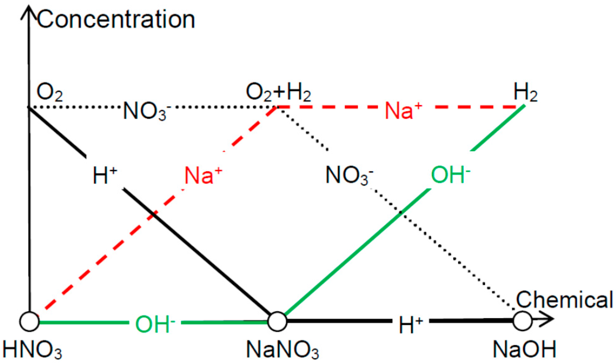
Figure 5 summarizes the effectiveness of exfoliation when using different electrolytes. In HNO
3 solution, NO
3− ions can screen OH
− at the backside of the metal foils and hence O
2 is peeling off the front side thin films. In NaOH, which is the other extreme, Na
+ screens H
+ so that H
2 can be used for the detaching. In the case of NaNO
3, both OH
− and H
+ are shielded and therefore O
2 and H
2 both contribute to the delamination (though H
2 is more effective due to the reasons listed above).
Other transitional situations, e.g., mixture, of HNO
3 and NaNO
3, can also be analyzed via relative weight analysis. Note that the relation [H
+]∙[OH
−] = K
w where K
W is the self-ionization constant of water cannot be reflected in this figure when [H
+] and [OH
−] are pushed towards the abscissa axis. Now let us look into the delamination efficiency when using reactions other than H
2O electrolysis. The Kolbe electrolysis is decarboxylative dimerisation of two carboxylic acids (or carboxylate ions):
such as 2CH
3COONa + 2H
2O = C
2H
6 + 2CO
2 + 2NaOH + H
2 (the effective ionic radii for COOH
− is 1.6 Å) [
16]. At a first glance, because the electrolyte CH
3COONa is also taking part in the redox reaction, one may expect it to give a better delamination efficiency. Also, at the anode, there are two types of gases (C
2H
6 and CO
2) with the total mole ratio to cathode H
2 being 3:1. Nevertheless, in experiments we find that the delamination efficiency at the anode is very poor (200 mL CH
3COONa solution at 0.25 mol/L), much worse than that for HNO
3 under the same conditions. This is because the solution is dominated by CH
3COO
− which is reactive (unlike NO
3−) and cannot offer a screening effect.
Figure 5.
Depending on the acidity or alkalinity of the water electrolysis solution, oxygen or hydrogen bubbles are effective in delaminating the thin films from their substrates (with uncovered backside).
Figure 5.
Depending on the acidity or alkalinity of the water electrolysis solution, oxygen or hydrogen bubbles are effective in delaminating the thin films from their substrates (with uncovered backside).
For simplicity, the discussion above only involves the delamination of bare PMMA thin films. Actually, we have repeated the experiments on Pt-grown graphene samples (spin-coated with a thin PMMA layer) and exactly the same screening effects are observed [
17]. Similar findings are found on Cu-grown graphene (although only connected as the cathode because Cu-anode will be electrochemically etched) [
17]. As we know, other interesting stable monolayers such as
h-BN, MoS
2,
etc. also demand a film transfer technology. We believe the screening effect is quite general and should be considered in the electrochemical delamination of all 2D materials beyond graphene. The bubbling separation process and the associated screening effect not only provide an ideal platform for surface science studies involving 2D materials, but also lead to economic and environmental benefits when it comes to applications. The metal foil catalysts used for 2D material growth are entirely reusable, drastically reducing the cost on raw materials and the heavy metal pollution. In the
Supplementary Material, we propose a roll-to-roll industrial process for the bubbling delamination of 2D materials from their metal catalysts, with the screening effect discussed above taken into account. Also, our speculation on the bubbling delamination of graphene from insulating SiC substrate is presented. This type of graphene is often called epitaxial graphene [
18,
19,
20,
21], where a reliable transfer of the graphene is highly desired.


