Article

A Dynamic Range Enhanced Readout Technique with a Two-Step TDC for High Speed Linear CMOS Image Sensors

School of Electronic Information Engineering, Tianjin University, 92 Weijin Road, Nankai District, Tianjin 300072, China
*
Author to whom correspondence should be addressed.
Sensors 2015, 15(11), 28224-28243; https://doi.org/10.3390/s151128224
Submission received: 31 August 2015 / Revised: 22 October 2015 / Accepted: 2 November 2015 / Published: 6 November 2015
(This article belongs to the Section Physical Sensors)

Abstract

:
This paper presents a dynamic range (DR) enhanced readout technique with a two-step time-to-digital converter (TDC) for high speed linear CMOS image sensors. A multi-capacitor and self-regulated capacitive trans-impedance amplifier (CTIA) structure is employed to extend the dynamic range. The gain of the CTIA is auto adjusted by switching different capacitors to the integration node asynchronously according to the output voltage. A column-parallel ADC based on a two-step TDC is utilized to improve the conversion rate. The conversion is divided into coarse phase and fine phase. An error calibration scheme is also proposed to correct quantization errors caused by propagation delay skew within −Tclk~+Tclk. A linear CMOS image sensor pixel array is designed in the 0.13 μm CMOS process to verify this DR-enhanced high speed readout technique. The post simulation results indicate that the dynamic range of readout circuit is 99.02 dB and the ADC achieves 60.22 dB SNDR and 9.71 bit ENOB at a conversion rate of 2 MS/s after calibration, with 14.04 dB and 2.4 bit improvement, compared with SNDR and ENOB of that without calibration.

Graphical Abstract

1. Introduction

Linear array image sensors obtain continuous images by scanning the target objects in one direction or in a loop, thus, they are usually used in industry detection, aerial photography, and satellite imaging. More and more applications require high speed scans to improve detection efficiency, and in some cases, the target objects are moving fast. Both conditions increase the demands of high line rate linear image sensors. Moreover, the target scene may contain high light and low light objects, and the dynamic range of the targets usually exceeds 90 dB. However, the dynamic range of traditional readout circuits is limited to 60–70 dB [1,2,3]. A wide dynamic range readout circuit is expected to cover at least a detecting range over 90 dB to capture all the possible information [1,4]. Therefore, the readout circuits of linear array image sensors require a wide detecting range and high speed readout.
For a linear CMOS image sensor (CIS), different types of readout techniques are used for various purposes, mainly including direct injection (DI), gate modulated injection (GMI), source follower per detector (SFD), and capacitor trans-impedance amplifier (CTIA) [5], etc. However, the integration linearity of DI and SFD gets significantly worse in dealing with wide range input signals. In GMI, the current gain and injection efficiency are sensitive to the threshold voltage change of MOS transistors, thus, readout circuits of different pixels may have large offset voltage [6]. Among these, CTIA can achieve good integration linearity and high injection efficiency, which makes it a popular readout circuit structure.
In order to fulfill the requirement of 90 dB photon dynamic range, a dynamic range extension technique has to be utilized. Various solutions for wide dynamic range CIS have been reported as CIS technology has developed. Some of them take advantage of improved pixel architectures, while others use novel readout methods. In general, they can be categorized into four main methods, i.e., logarithmic response, well capacity adjustment, multiple sampling, and saturation detection [7,8,9]. Well capacity adjustment and saturation detection are usually used in 4-T pixels. Logarithmic response and multiple sampling methods can be used with CTIA readout circuits. However, multiple sampling needs two or more times the readout operations than traditional pixels, which significantly limits the line rate. Logarithmic response is a simple and effective way, however, it suffers from fixed pattern noise when applied to APS. Therefore, a logarithmic-like response curve is created with a new CTIA-based dynamic range extension technique to achieve over 90 dB photon dynamic range.
High speed ADC is also necessary to achieve high line rates. Column-parallel ADC is the most widely used architecture in high speed linear imagers because it provides a better tradeoff among readout speed, silicon area and power consumption. Currently, three types of column-parallel ADCs have been used in CMOS image sensors: a successive approximation (SAR) ADC [10,11], a cyclic ADC [12], and a single-slope (SS) ADC [13,14]. Compared with SAR and cyclic ADCs, SS ADCs have many attractive features such as good linearity, simplicity of the analog circuits and resulting suitability for fine-pitched pixels. Moreover, they can ensure uniformity between columns and thus minimize column FPN. However, it may be difficult to simultaneously achieve both high-speed A/D conversion and high bit resolution because the required conversion time increases by a factor of 2N for N-bit resolution. To improve the conversion speed, some new methods have been reported: two-step single-slope ADC [15,16,17], multiple-ramp multiple-slope (MRMS) ADC [18], etc. In addition, further reduction in conversion time can be achieved by time-based SS ADC [19]. The input signal is converted to a time-domain representation using a ramp generator and a comparator and then the time domain information is quantized by a time-to-digital converter (TDC).
This paper presents a dynamic range enhanced, high speed readout technique consisting of a CTIA type readout circuit and a column-parallel SS ADC with two-step TDC. The proposed ADC has a significantly increased conversion rate compared with the conventional SS ADC [13,14], and costs less power and area than the multiple-ramp ADC [20].
The rest of this paper is organized as follows: Section 2 describes dynamic range enhanced column readout circuits as a preliminary to the following sections. Section 3 discusses the detailed design and operation of proposed ADC, a calibration technique to mitigate the impact of mismatch in the two-step TDC is also presented. Section 4 presents the results, and Section 5 provides the conclusions.

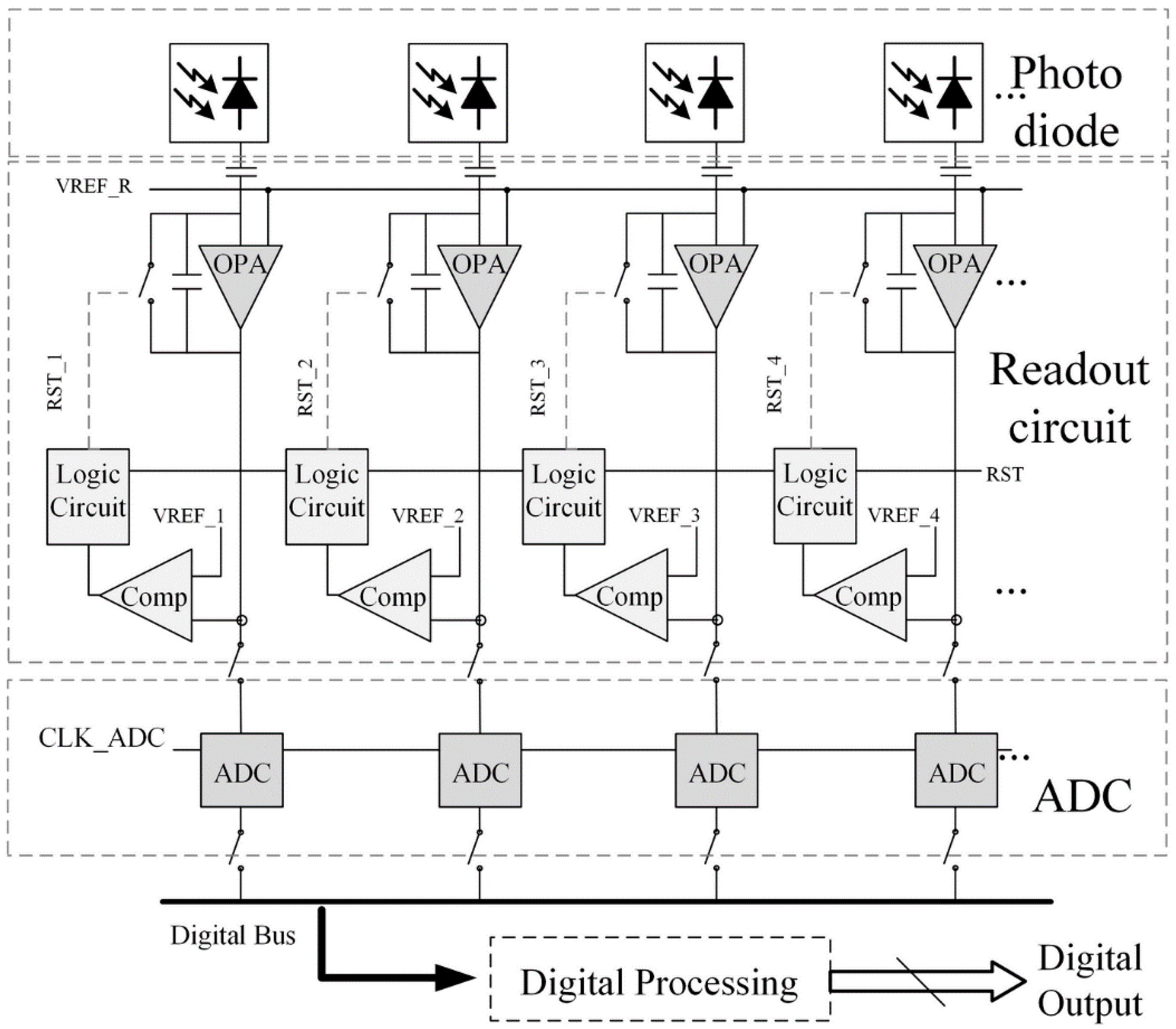
2. Dynamic Range Enhanced Readout Circuit

The architecture of a linear image sensor with dynamic range enhanced readout circuits and two-step TDC based ADCs is shown in Figure 1. It consists of a linear photodiode array, dynamic range enhanced readout circuits, analog to digital converters, and peripheral circuits. The photodiode and readout circuit compose a pixel in the conventional sensors.
Figure 1. Block diagram of a linear image sensor.
Sensors 15 28224 g001

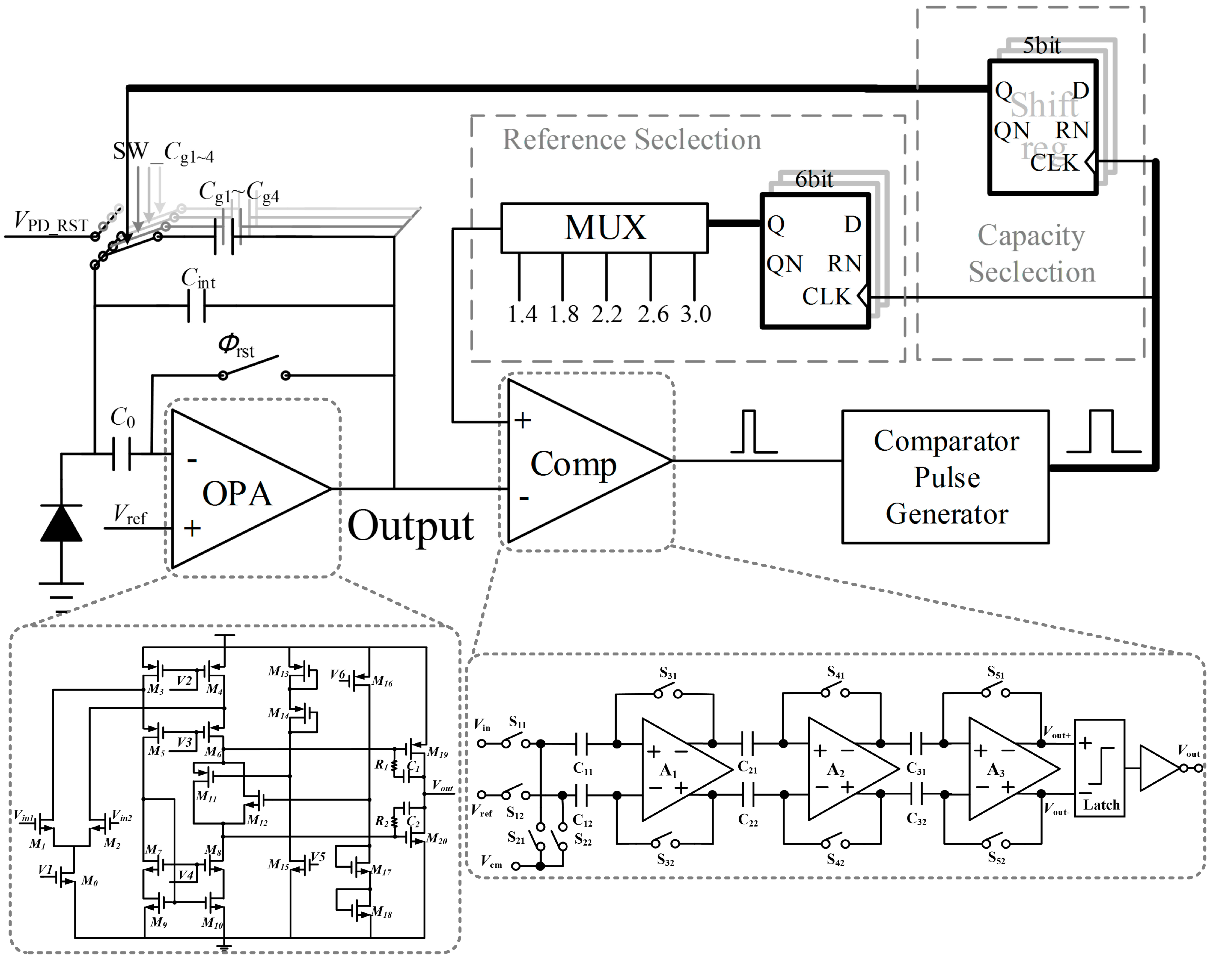
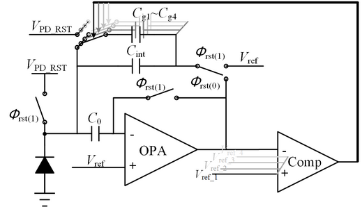
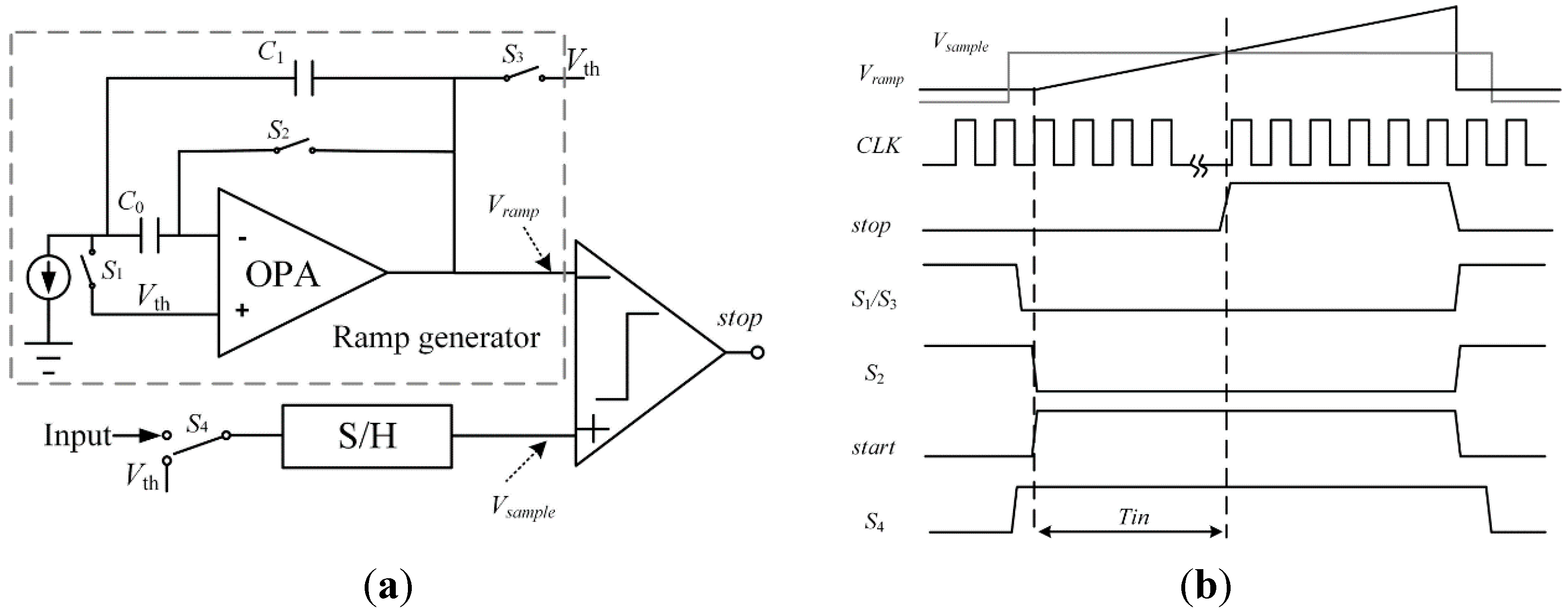
2.1. Capacitor Trans-Impedance Amplifier (CTIA)

An improved CTIA structure is developed as the readout circuit in this paper due to its wide detection range, low noise and good integration linearity. Moreover, the non-destructive readout (NDR) can be realized with the CTIA structure. NDR mode is similar to the standard readout mode except that the output signals can be read out multiple times in a single readout integration time. The CTIA isolates the photodiode and the output signals by an amplifier, thus the readout operation does not have any effect on the photodiode.
The structure of CTIA is shown in Figure 2, where the integration capacitor is placed on the feedback loop of the amplifier with a reset switch to initialize the integration capacitor and reset the output to Vref. Additional integration capacitors Cg1 to Cg4 are connected to the circuit in parallel with Cint. The left plates of Cg1 to Cg4 are connected to VPD_RST in reset phase. A comparator at the output node is used to judge different reference voltages and control the amount of integrating capacitors accessing to CTIA at integration period. This CTIA-based structure has offset cancellation ability and dynamic range extension function.
Figure 2. (a) The structure of CTIA; (b) The output curve of CTIA.
Sensors 15 28224 g002

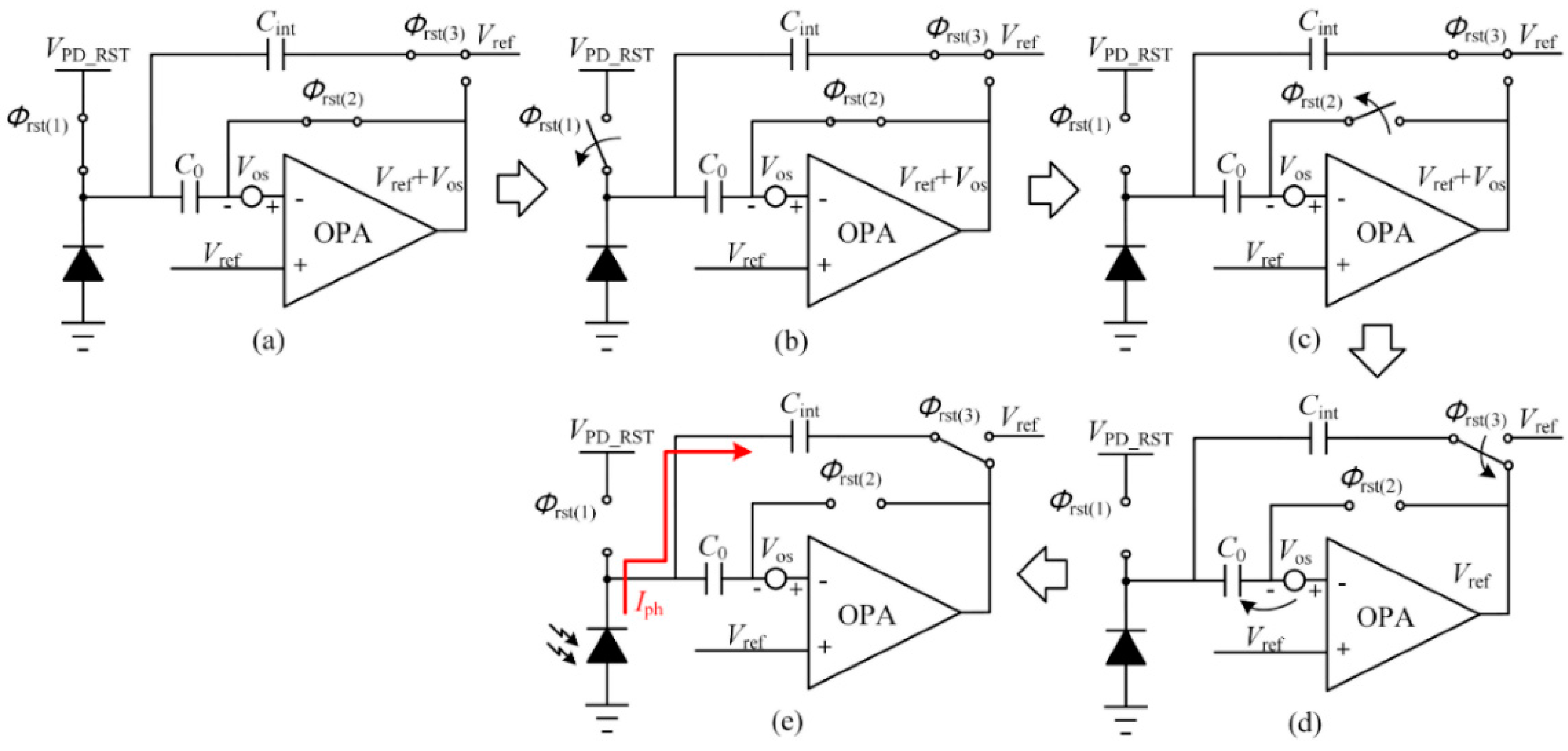
2.1.1. Offset Cancellation

Device mismatch and process variations may lead to offsets among pixels. A conventional CTIA-based pixel resets the photodiode by shorting the negative input and output of the OPA [21]. This method is simple, but an offset voltage induced by the OPA exists at the output, which is one of the sources of fixed pattern noise in pixel arrays. In this design, a reset transistor, an extra capacitor C0 and a Single Pole Double Throw (SPDT) switch are adopted to eliminate the offsets at the output, also make the reset voltage of the photodiode flexible.
The switch sequence is shown in Figure 3. During the reset period, Φrst(1)–(3) signals are set as the logic high level to turn these switches on, as shown in Figure 3a. At the reset period, the photodiode is reset to VPD_RST, and the negative input and the output of the OPA is reset to Vref + Vos, where Vos represents the offset voltage induced by the mismatches in the OPA. At the same time, the right plate of the integrating capacitor is always connected to Vref.
The reset phase ends as Φrst(1) transits to its low level first as Figure 3b shows. KT/C noise is integrated on the photodiode, but it cannot propagate to the output as the right plates of Cint and C0 are still clamped. Then Φrst(2) transits to its low level as Figure 3c shows. The offset voltage is stored on C0 while Vout remains as Vref + Vos. When Φrst(3) is switched to the output of the OPA as shown in Figure 3d, because the charge stored on the integration capacitor Cint and C0 remains and they form a negative feedback, Vout turns from Vref + Vos to Vref. In fact, the accurate value of Vout is:
V out = V ref V os A 1
where A is the open-loop gain of the OPA in the CTIA structure. By considering the load effect of the capacitors, the frequency expression of the open-loop gain in a two-stage OPA is:
A ( s ) =  A 0 ( 1 + R I C I s ) ( 1 + R II C II s )
where A0 is the open-loop DC gain, RI (RII) and CI (CII) are the resistance and capacitance to ground seen from the output of the first (second) stage. The capacitance load at output is derived as:
{ C II ( reset phase )  =  C int C II ( integration phase )  =  ( C 0 C in C 0  +  C in  +  C pd ) C int ( C 0 C in C 0  +  C in  +  C pd ) + C int C 0 C in C 0 + C in  +  C pd
where Cin is the parasitic capacitance of input terminal, and Cpd is the parasitic capacitance of the photodiode. Since they are not large capacitance load, the OPA may achieve a good transient response characteristic easily. Furthermore, when the signal settles, the open-loop gain at low frequency is extremely large. Therefore, in Equation (1), the latter term is so small that it should be omitted, i.e., the offset voltage at output terminal is cancelled. Then the CTIA structure starts to integrate the photo current Iph on the integration capacitor Cint from Vref. Since the OPA is not ideal, its gain and the parasitic capacitance of the photodiode should be taken into consideration. Then the output voltage is derived as:
V out = A 1 + A ( V ref + ( A 1 ) I ph t ( A 1 ) C int + C pd )
where t is the integration time. From the equation above, if A is large enough, the expression of Vout can be simplified as:
V out = V ref + I ph t / C int
Figure 3. Switch sequence of the offset cancellation scheme. (a) Reset state; (b) ϕrst(1) is switched off; (c) ϕrst(2) is switched off; (d) ϕrst(3) is switched from Vref to the output terminal; (e) Iph starts to integrate on Cint.
Sensors 15 28224 g003

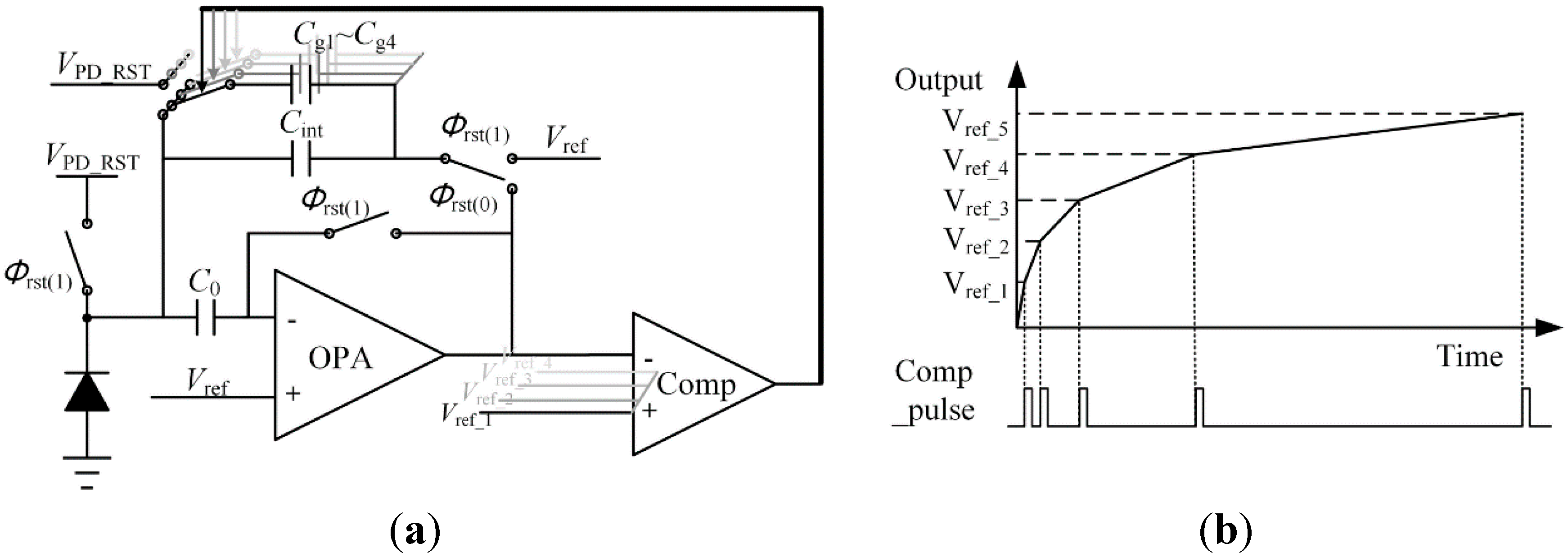
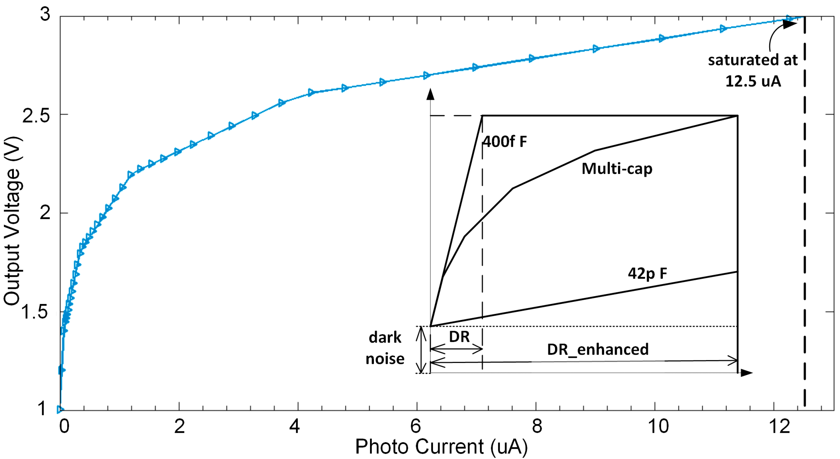
2.1.2. Dynamic Range Extension

In the conventional integration, the output increases linearly and saturates at Vsat as Equation (5). CTIA operates as an integration circuit for photodiode. The photocurrent integrates on the capacitors connected across the input and output terminal which determines the sensitivity of integration. Sensitivity here is defined as the voltage variation under the conditions of 1 A photo current and 1 s integration time. Then the sensitivity could be derived from Equation (5) as:
S = 1 C int
High sensitivity of integration can be achieved by using a small capacitance, and a large capacitance achieves the opposite [22]. A good sensitivity could improve the ability of low light detection and achieve low equivalent input noise, but it gets saturated under high light conditions. To address this issue, a multi-capacitor and self-regulation method is applied to the CTIA structure to achieve the wide dynamic range feature. Several capacitors, Cg1 to Cg4 in this design, are connected into the circuits in parallel with Cint as additional integration capacitors. A reusable comparator is connected to the output terminal of the CTIA to monitor the signal voltage. The corresponding reference voltages, Vref1 to Vref5 are delivered by a MUX to the input terminal of the comparator. The sensitivity of the CTIA is automatically adjusted by switching different capacitors to the integration node asynchronously according to the output voltage. This method extends the dynamic range by compressing the photo response in the high light region as shown in Figure 2b. With a logarithmic-like photoresponse curve, the output under high light conditions would not get saturated compared to the traditional design with a single integration capacitor. Then both low and high light information is acquired.
The principle of this dynamic range extension approach is detailed as follows. When the reset phase ends, the photocurrent begins to integrate on Cint, and Vout grows upward from Vref. During the integration period, the comparator keeps monitoring Vout, and the reference voltage is set as Vref1 at first. Once the signal voltage reaches the reference voltage Vref1, a short pulse is generated to switch Cg1 to the integration node. Thus, the integration capacitance increases and the sensitivity gets lower. After these operations, the reference voltage connected to the comparator is switched to the next predetermined voltage, Vref2, and then the comparator continues to monitor the signal and repeats the operations above. Assuming that light intensity is constant, then the output voltage of the CTIA is:
V out  =  I ph i =  1 n t i C total _ i + V ref
where ti is the integration time of i-th segment, and Ctotal_i is the total capacitance used for photo current integration.
Thus, the sensitivity of each integration segment is:
S i  =  1 C total _ i
In the proposed design, four additional capacitors, Cg1 to Cg4, are to be connected to the integration node, and five reference voltages (including a saturation voltage) are alternately applied to the comparator. Then the photo response curve becomes a polyline with five segments before it gets saturated. The output swing in this design is from 1 V to 3 V, which is divided into five segments, thus the reference voltages are 1.4, 1.8, 2.2, 2.6 and 3.0 V, respectively.

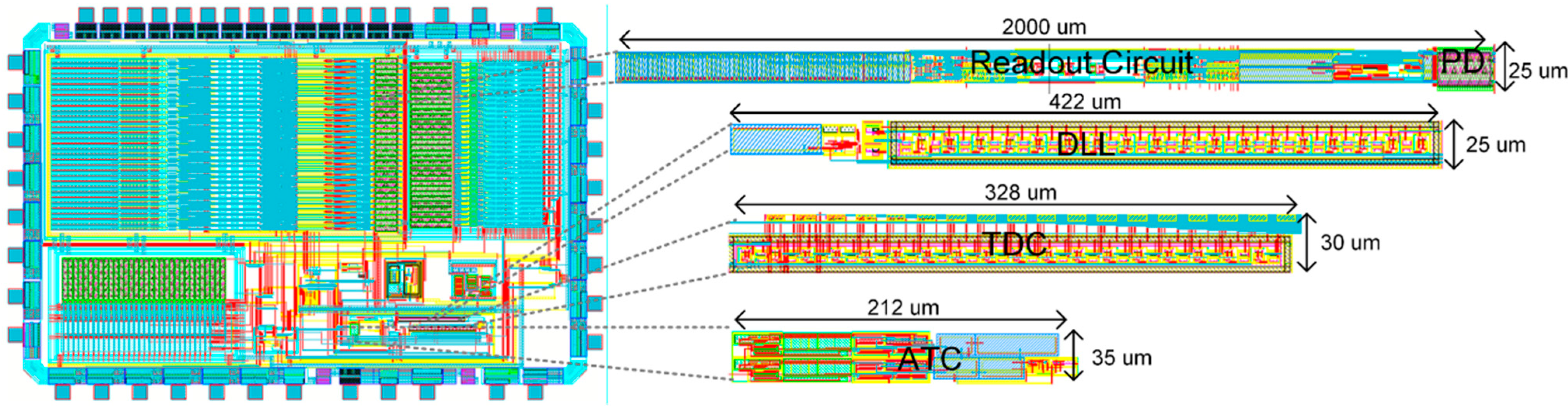
2.2. Readout Circuits Implementation

In this design, a polyline type photoresponse curve with five segments is expected. The slope ratios of two adjacent segments are assumed to be equal. Then the slope ratio k can be calculated by:
k = 1 +  C n i = 0 n-1 C i ( 0 n 4 )
where n is the number of capacitors, Cn is the n-th capacitor that connected to the integration node. Each capacitance can be calculated by detection range and k. In this design, we define the maximum saturate current I0 to be around 12 μA within an integration time of 2 μs as the target. The slope ratios of two adjacent segments are assumed to be equal, and the voltage swing of the readout circuit is 2 V. According to these conditions, k is figured out to be 3.21. The initial capacitance is 400 fF, then four additional capacitors C1C4 are 0.88 pF, 2.84 pF, 9.02 pF, and 29.03 pF. The total capacitance is 42.17 pF.
In order to capture clear image in fast scan application, the integration time in this design is as short as 2 μs. The maximum saturation current I0 during this time is 12.3 μA, then the maximum charging current Itotal_max at the first integration segment is given by:
I total_max = I 0 × C total C 0
From Equation (10), Itotal_max is around 1.3 mA, i.e., the CTIA has to output 1.3 mA current to drive all these capacitors.

2.2.1. OPA Design

The OPA should be carefully designed to obtain such a large output current and reduce quiescent current as well. As shown in Figure 4, a class AB output stage is employed in OPA design. In order to achieve high speed detection, the amplifier may need to supply significant amounts of current to rapidly charge the load to the target accuracy. Therefore, an OPA with high gain, large output current, and low quiescent current is required. In this design, the OPA with class AB output stage achieves 102 dB gain and over 1.3 mA output current with a 130 μA quiescent current.

2.2.2. Logic Control and Comparator Design

As shown in Figure 4, the control logic circuit is mainly composed of a pulse generator (PG), a reference voltage selector (RVS) and an integrating capacitor selector (ICS). PG is used to broaden the width of the reset pulse generated by the comparator when it is triggered. RVS delivers the corresponding reference voltage to the input of the comparator. ICS controls the amount of integrating capacitors accessing to CTIA for integration.
To acquire an accurate integrated voltage, the comparator should have sufficient gain, as well as the smallest propagation delay. The comparator uses three cascaded low-gain amplifiers as the preamplifier and a latch at the output, as shown in Figure 4. An offset cancellation technique is utilized to compensate the offsets of these amplifiers. As a result, the input offset of the comparator can be reduce to less than 0.5LSB.
Figure 4. Circuit diagram of CTIA.
Sensors 15 28224 g004

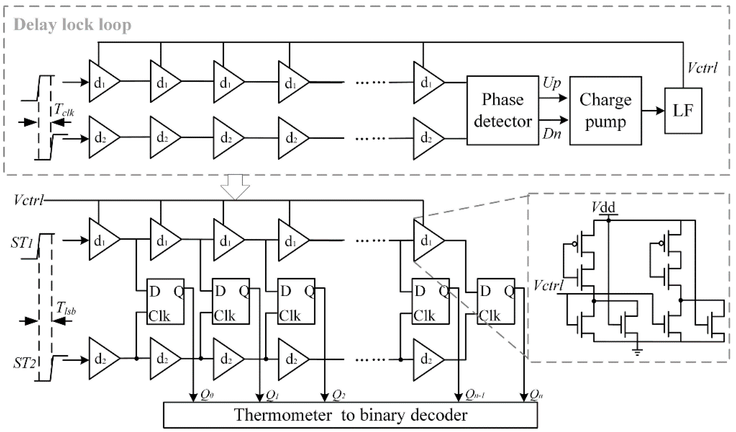
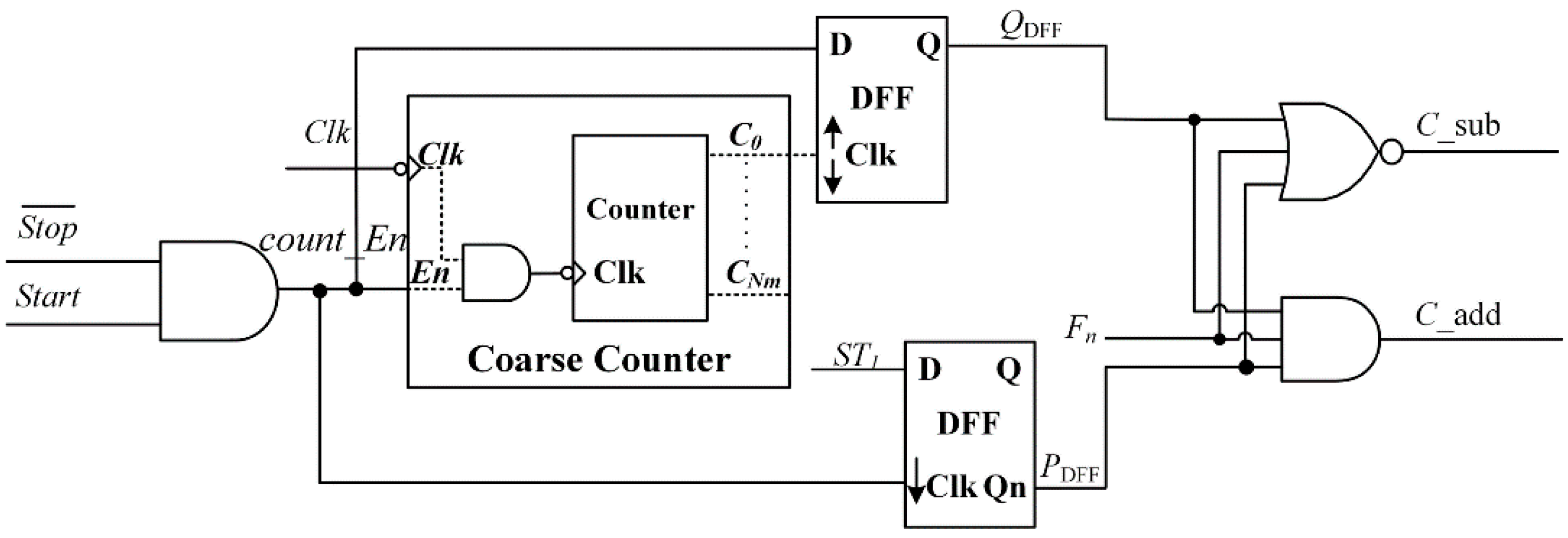
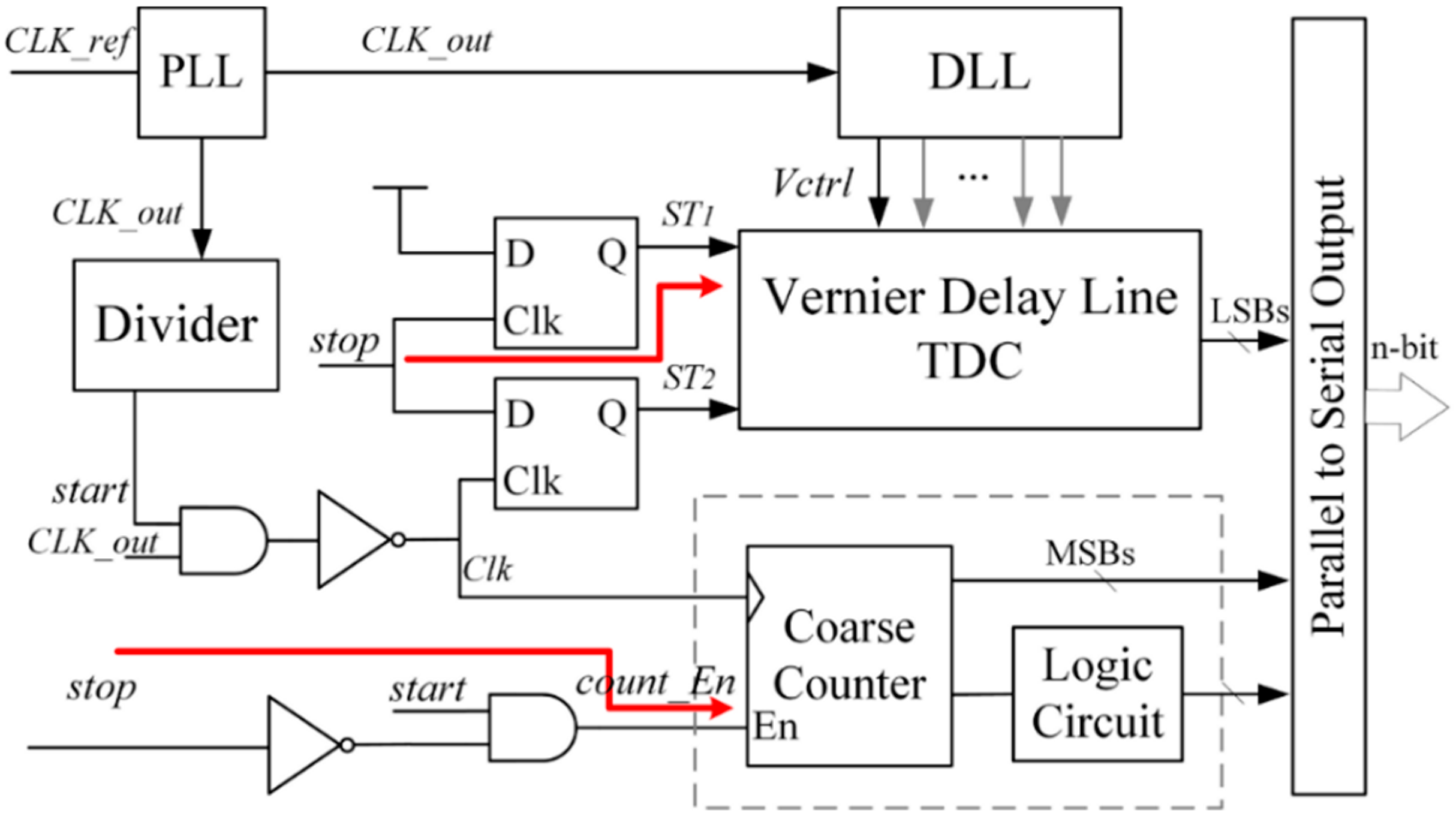
3. Design of Column-Level ADC with Two-Step TDC

The conventional column-level ADC usually operates at a relatively slow conversion speed. To achieve both wide dynamic range and high conversion rate, with low power consumption, a two-step TDC is utilized in this design.

3.1. Operation Principle
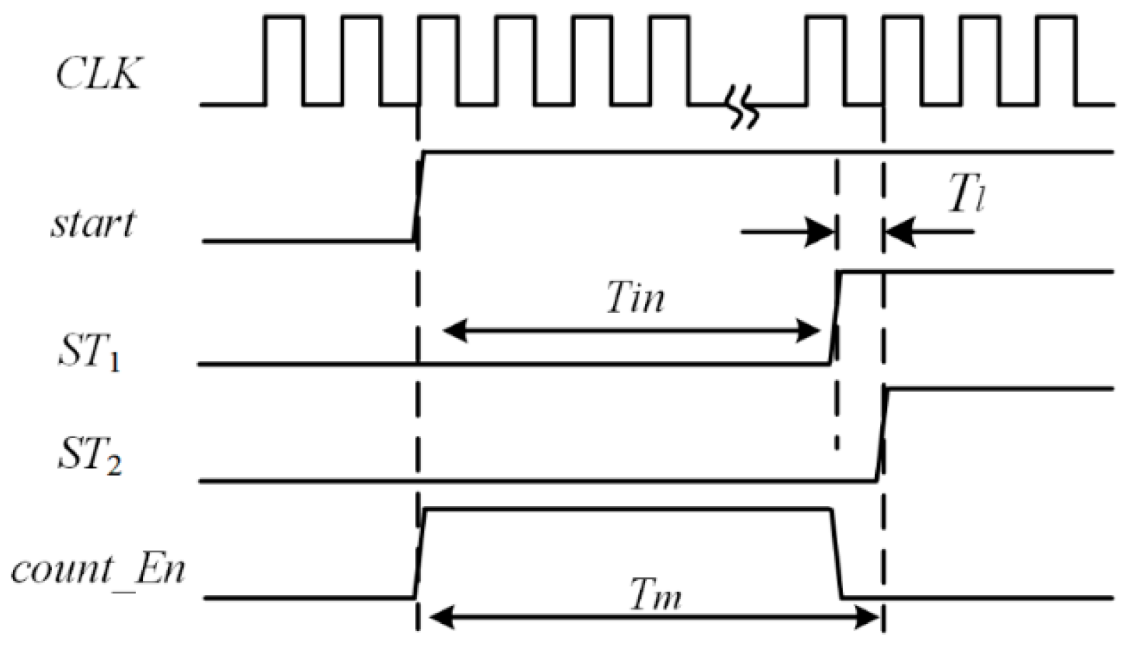
The basic concept of the proposed ADC consists of an analog-to-time conversion (ATC) and a parallel two-step TDC. The ATC transforms the sampled input voltage into a pulse signal whose width is linearly proportional to the input voltage. Then the width of the pulse signal is measured by the parallel two-step TDC, which yields a corresponding digital output. The n-bit conversion process of TDC is divided into m-bit coarse and l-bit fine conversions, where n = m + l. The coarse quantization is implemented by a counter which consumes little power, and the fine quantization is performed by a Vernier delay line (VDL) to obtain good accuracy [23]. By using this two-step architecture, the power consumption of TDC is reduced while maintaining large quantization range and fine resolution. The key challenges of this architecture are to achieve an efficient two-step TDC circuit architecture and ensuring the synchronization of two-step quantization.

3.2. ATC

Figure 5 shows the block diagrams and timing diagrams of the suggested linear ATC, which is composed of a sample-and-hold circuit, a ramp generator and a comparator. The linearity of ATC directly affects the ADC resolution [20]. In this design, OPA is used in the circuit to generate ramp voltage from 1 V to 3 V. Compared with [20], the nonlinearity caused by the finite resistance of current source could be avoided as long as the gain is large enough.
The timing diagram of ATC is shown in Figure 5b. The switches, S1, S2 and S3, are controlled by the start signal, which is generated by the timing module. When the start signal rises up to high level, Vramp begins to grow upward from Vth. The switch S4 is controlled by sample signal, which arrives a little earlier than the start signal. When Vsample and Vramp intersect, the comparator generates a pulse. Assuming that the ramp slope is constant, the time span between the start of the ramp and the comparator pulse is linearly proportional to the input voltage. The output signal of comparator is used as stop signal for TDC and the time interval Tin which will be quantized is between the rising edge of start and stop signals.
Figure 5. (a) Block diagram of ATC; (b) Timing diagram of ATC.
Sensors 15 28224 g005

3.3. TDC

To achieve both energy efficiency and a large dynamic range, a two-step TDC combining a coarse counter and a VDL TDC is proposed. As shown in Figure 6, it is mainly composed of a VDL TDC, a coarse counter, a PLL that stabilizes clock frequency and a DLL to provide control voltages for VDL. A coarse counter quantizes the input time interval coarsely, and the residue is injected into a VDL TDC for fine quantization. Three more signals are introduced to describe the principle well: the start of fine quantization ST1; the stop of fine quantization ST2; and the enable signal of coarse quantization count_En. ST1 is set by the rising edge of stop signal. ST2 is set by the next rising edge of clock after the stop signal. count_En is set by start and reset by stop. Figure 7 shows the timing diagram of the two-step operation. A coarse counter measures the number of reference clock cycles while the count_En signal is high, i.e., it measures Tm. The time interval between the rising edges of ST1 and ST2, defined as Tl, is measured by the fine TDC. As shown in Figure 7, the width of the input interval, defined as Tin, is calculated by:
T in = T m T l
Figure 6. Block diagram of proposed TDC.
Sensors 15 28224 g006
Figure 7. Timing diagram of proposed TDC.
Sensors 15 28224 g007
The structure of VDL is shown in Figure 8, it consists of two delay-lines: One for the ST1 and the other for ST2. The up-line is composed of voltage-control delay elements and the down-line is composed of fixed delay elements. It is noted that the signal arrival time uncertainty grows with the length of the delay line. If more than 40 stages are implemented in the VDL, manufacture variations are the major sources of errors affecting the linearity. Sixteen stages are chosen for each delay line to quantize Tl.
The delay elements in the up-line have a delay td1 which is slightly longer than the delay td2 of the elements in the down-line. Thus, when the comparator output stop signal arrives, the ST2 chases the ST1. In each stage the delay difference is shortened by:
t d = t d 1 t d 2
The order status of two signals is detected by D flip-flops, and the output Q1Q2Qn will be “11…00”. Assuming that the amount of “1” is L, then the interval of fine quantization is:
T l  =  L × t d    =  L × ( t d 1 t d 2 )    =  L × T clk 2 N l
Finally, this thermometer code will be translated to binary code and l-bits digital output is generated.
Thus the TDC output can also be expressed as:
T in = T m T l     = M × T clk L × T clk 2 N l
where M is the coarse counter output.
However, the delay difference is uncertain as the digital delay elements depend on process variations, temperature, and supply voltage (PVT variations). The best way to stabilize the value of Δtd against PVT variations and also provide calibration against process variations is to utilize Delay Lock Loop (DLL). DLL has two delay lines just the same as that in TDC as shown in Figure 8. Two similar signals only with one period time offset are injected into the delay lines, respectively. The output signals of the two delay lines are fed to a phase detector (PD) that compares the phase of these periodic signals. The phase detector generates a bias voltage Vctrl based on the phase difference to control the delay time, so that the delay of each element can be tuned by its control voltage Vctrl, and eventually the TDC resolution is locked to: Δtd = Tclk/N. A dummy DFF is also implemented in the DLL to balance the loading of the delay elements in the DFF.
Figure 8. Block diagram of VDL and DLL.
Sensors 15 28224 g008

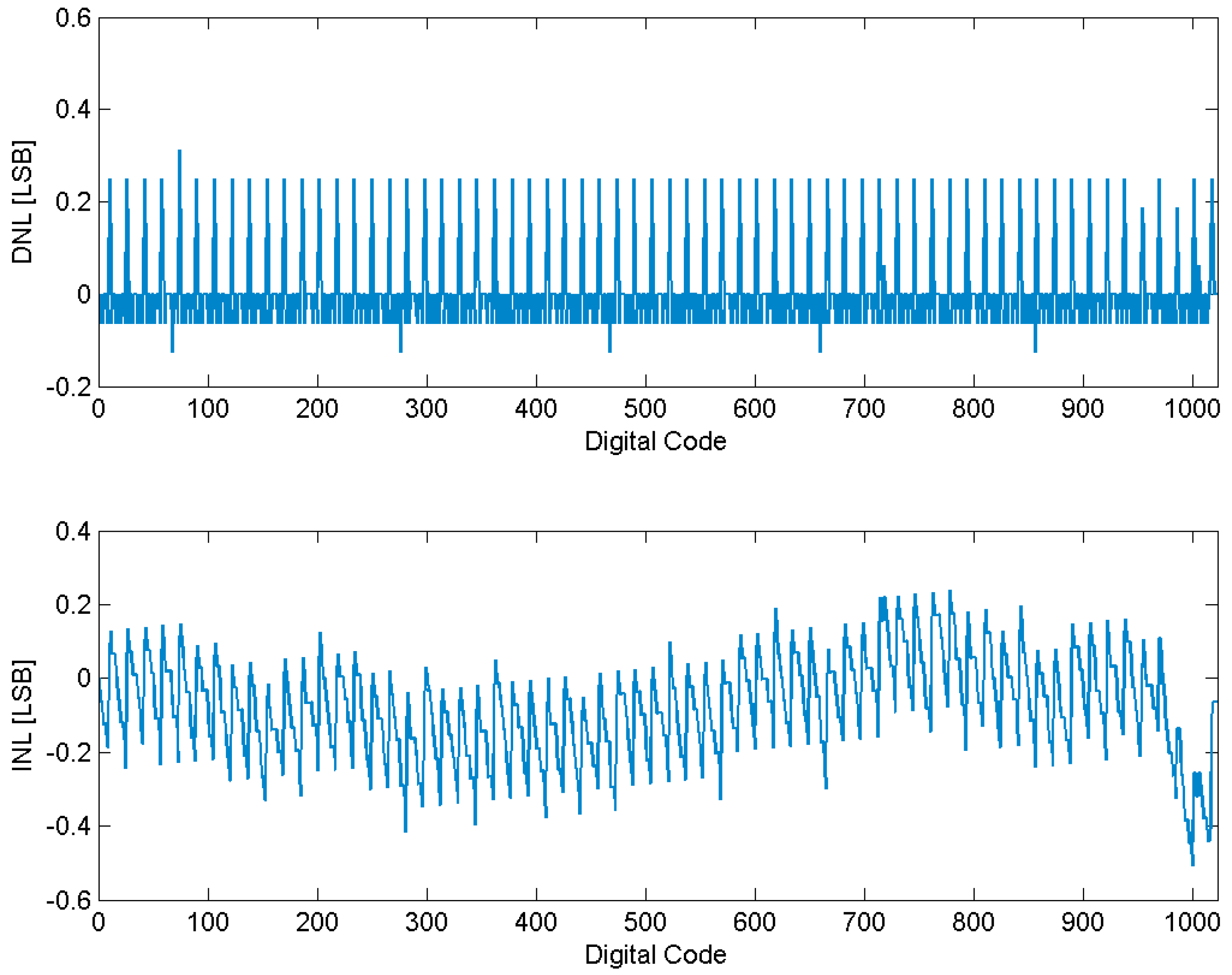
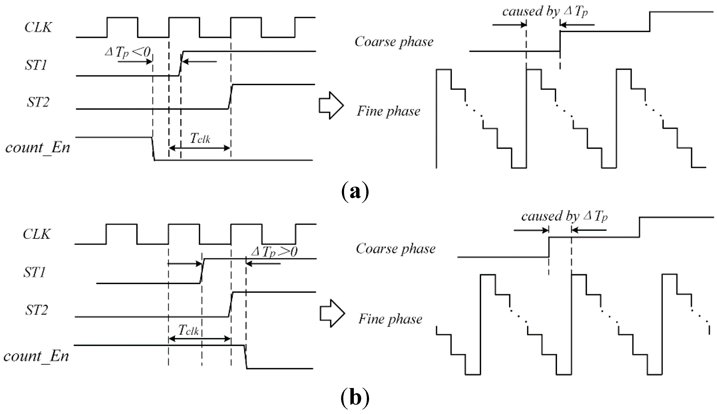
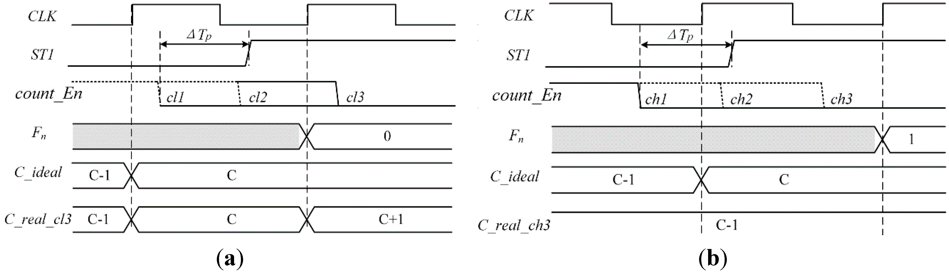
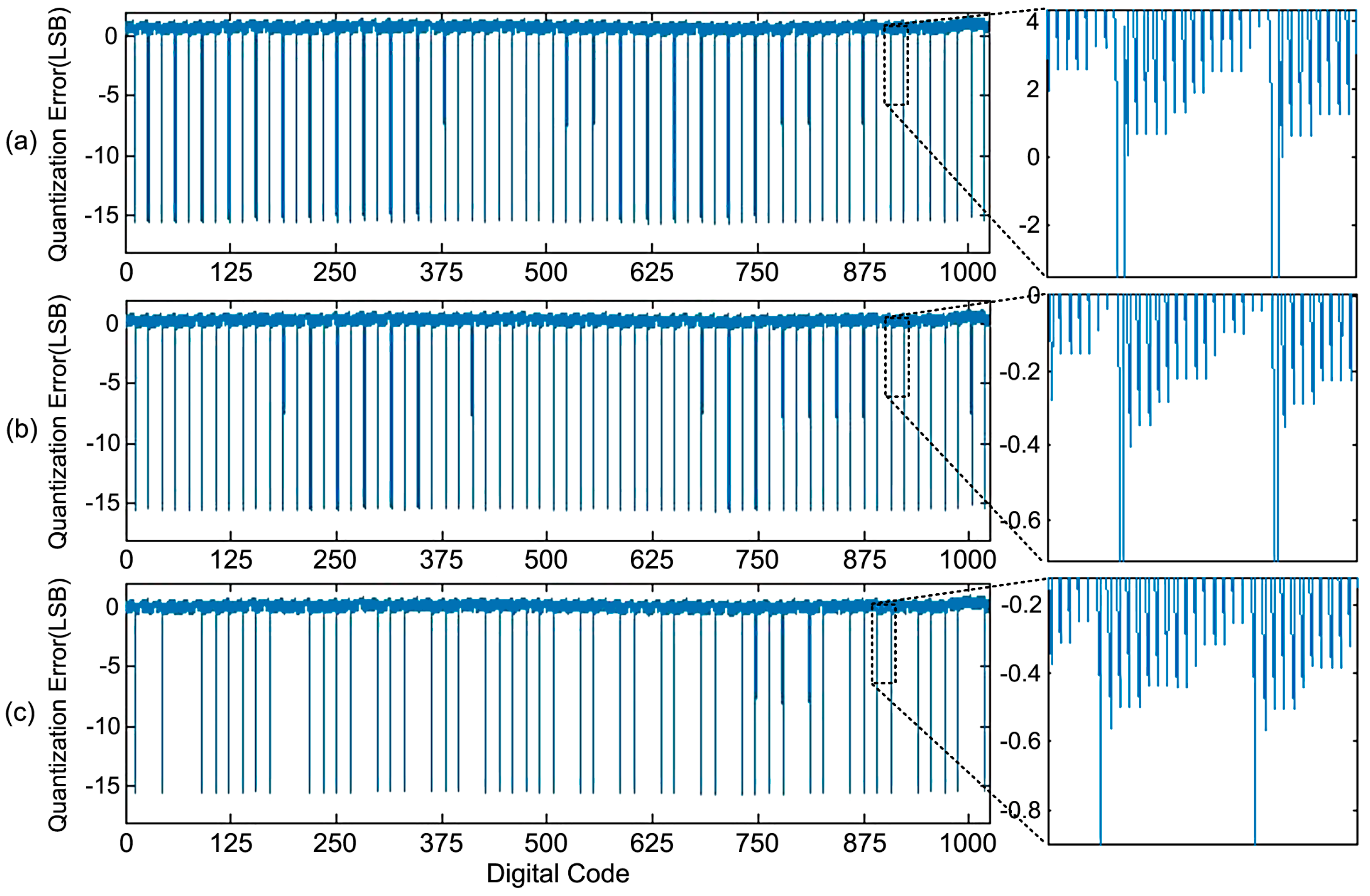
3.4. Quantization Error and Calibration

For the proposed two-step TDC, the coarse quantization and fine quantization process the input signals in parallel and generate real-time outputs, the synchronization of input signals propagation should be guaranteed. This implies that the falling edge of stop signal of coarse quantization count_En must occur in the fine quantization cycle, or the quantization results may have a one-bit coarse quantized error. However, the delay time difference caused by device mismatches and process variations between different propagate paths make it impossible to align the coarse and fine quantization correctly. The quantization errors occur in two conditions, as shown in Figure 9. As depicted in Figure 9a, when the edge of count_En is coming before rising edge of the fine quantization clock cycle, the actual result of coarse quantization is 1LSB less than ideal result. On the contrary, when the edge of count_En is coming after the fine quantization clock cycle, the actual result of coarse quantization is 1LSB more than ideal result. Therefore, it causes quantization errors and seriously affects linearity.
Some latency can be compensated by additional elements in the propagate path, but additional delay elements also mean additional variability, additional power, and additional noise. In this paper, a calibration method is proposed to eliminate the quantization error with less additional circuits. As shown in Figure 9, the time latency between count_En and ST1, is defined as ΔTp, and the reasonable range of ΔTp is −Tclk~+Tclk.
Figure 9. Timing diagrams of the TDC illustrating quantization error sources. (a) ΔTp < 0; (b) ΔTp > 0.
Sensors 15 28224 g009
As depicted in Figure 10a, when ST1 rises at the low level state of clock, the edge of count_En signal may appear in three positions cl1,cl2,cl3, which indicate that the range of latency is 0~+Tclk, −Tclk/2~+Tclk/2, −Tclk~0, respectively. When ST1 rises at the high level state of clock, the edge of count_En signal may appear in three other positions ch1,ch2,ch3, which indicate that the range of latency is 0~+Tclk, −Tclk/2~+Tclk/2, −Tclk~0, respectively.
The proposed calibration circuit is illustrated in Figure 11, which is composed of a double input AND, a counter, a double edge-triggered D flip-flop, a falling edge-triggered D flip-flop, a triple input AND and a triple input NOR. The counter is modified as falling edge triggered, thus the last change in the LSB of the counter, C0, could be caused by the edge of count_En signal. Compensation for coarse quantization result is decided by analyzing logic levels of clock and ST1, when stop signal propagate to the coarse or fine quantization. The double edge-triggered DFF is used to obtain the state of count_En signal when C0 changes. The falling edge-triggered DFF obtains the state of ST1 when count_En falls. Furthermore, the MSB of fine quantitative output, denoted as Fn, is utilized. In the case of Fn = 0, as shown in Figure 10a, which means ST1 rises at the low level state of clock. If the falling edge of count_En signal appears in position cl3, which is at the high level state of the clock, the last change of C0 comes from the falling edge of count_En, and the final output of DFF, QDFF = 0. In addition, ST1 signal is in the high level when count_En changes, and it means the reverse output of DFF, PDFF = 0. Then the C_sub generated by “NOR” operation is high, thus it will subtract 1LSB from the coarse quantization output. Similarly, when the falling edge of count_En signal is in position cl1 or cl2, the correction bit C_sub and C_add are equal to 0, which means no need for calibration. On the contrary, ST1 rises at the low level state of clock as shown in Figure 10b, in this case, Fn = 1. If the falling edge of count_En signal is in position ch1, which is in the low level of the clock, the last change of C0 comes from the falling edge of clock, and the final output of DFF, QDFF = 1. In addition, ST1 signal is in the low level when count_En changes, and it means the reverse output of DFF, PDFF = 1. Then the C_add generated by “AND” operation is high, thus it will add 1LSB to the output. There is also no need for calibration when the falling edge of count_En signal is in position ch2 or ch3.
Figure 10. Timing diagram of the proposed calibration circuit. (a) ST1 rises at the low level state of clock; (b) ST1 rises at the high level state of clock (C_ideal denotes the ideal output of coarse quantization; C_real denotes the actual output of coarse quantization).
Sensors 15 28224 g010
Figure 11. Block diagram of the proposed calibration circuit.
Sensors 15 28224 g011
The proposed calibration method can effectively compensate the coarse quantization error caused by delay skew within −Tclk~+Tclk with a slight increment of area and power consumption.

4. Results

A linear CMOS image sensor with 32 × 1 pixel array is designed in the 0.13 μm CMOS process. The small-scale array is designed to prove the validity of readout circuits, and the pixel array could be extended, since the proposed readout circuits and ADCs are column wise designs. Figure 12 shows the layout of the linear image sensor. Each column readout circuit consumes 693 μW, and the ADC consumes 355 μW power consumption provided by a 3.3 V supply for the analog circuits and a 1.5 V supply for the digital blocks. The following results are all from post-layout simulation.
Figure 12. Layout of the linear image sensor.
Sensors 15 28224 g012

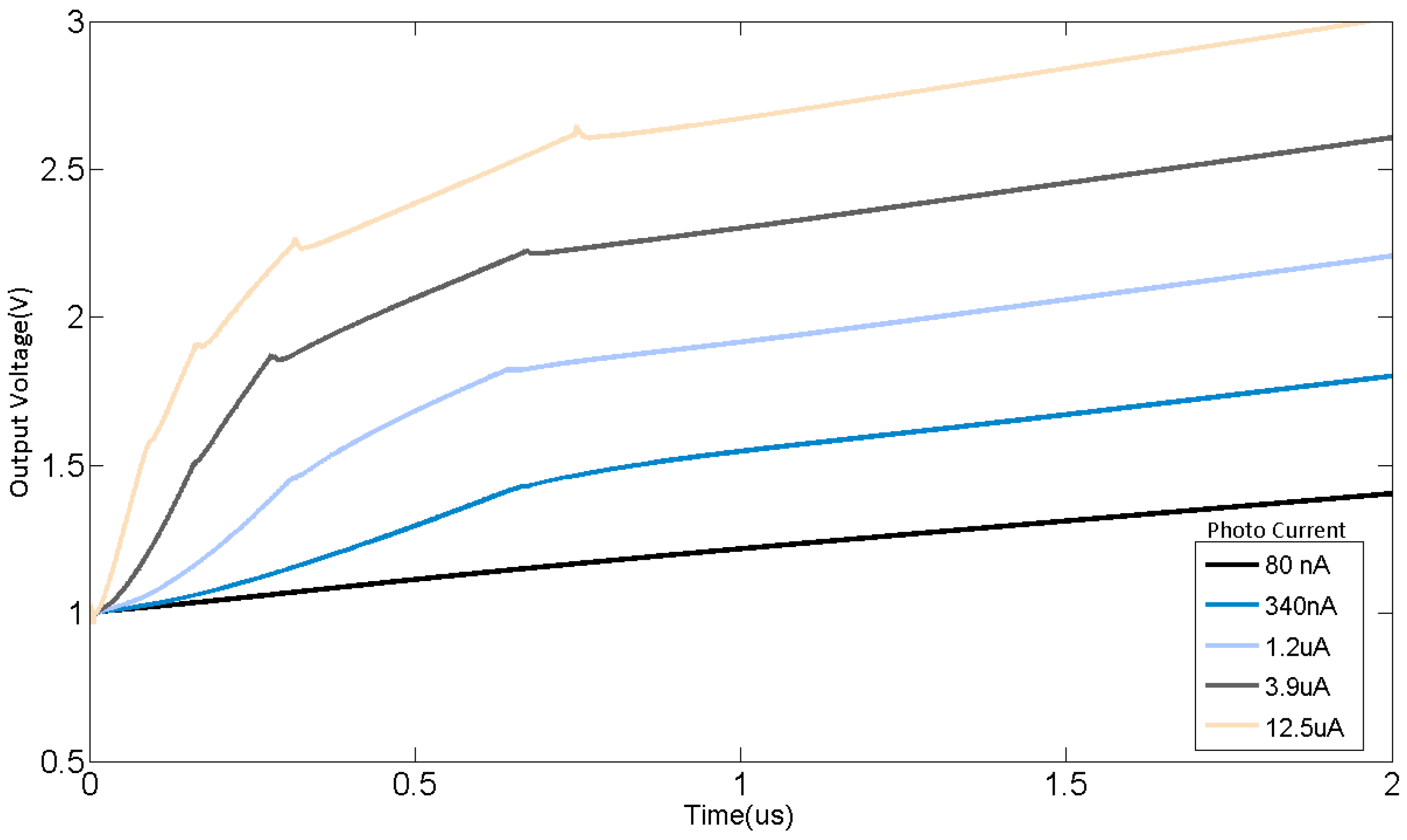
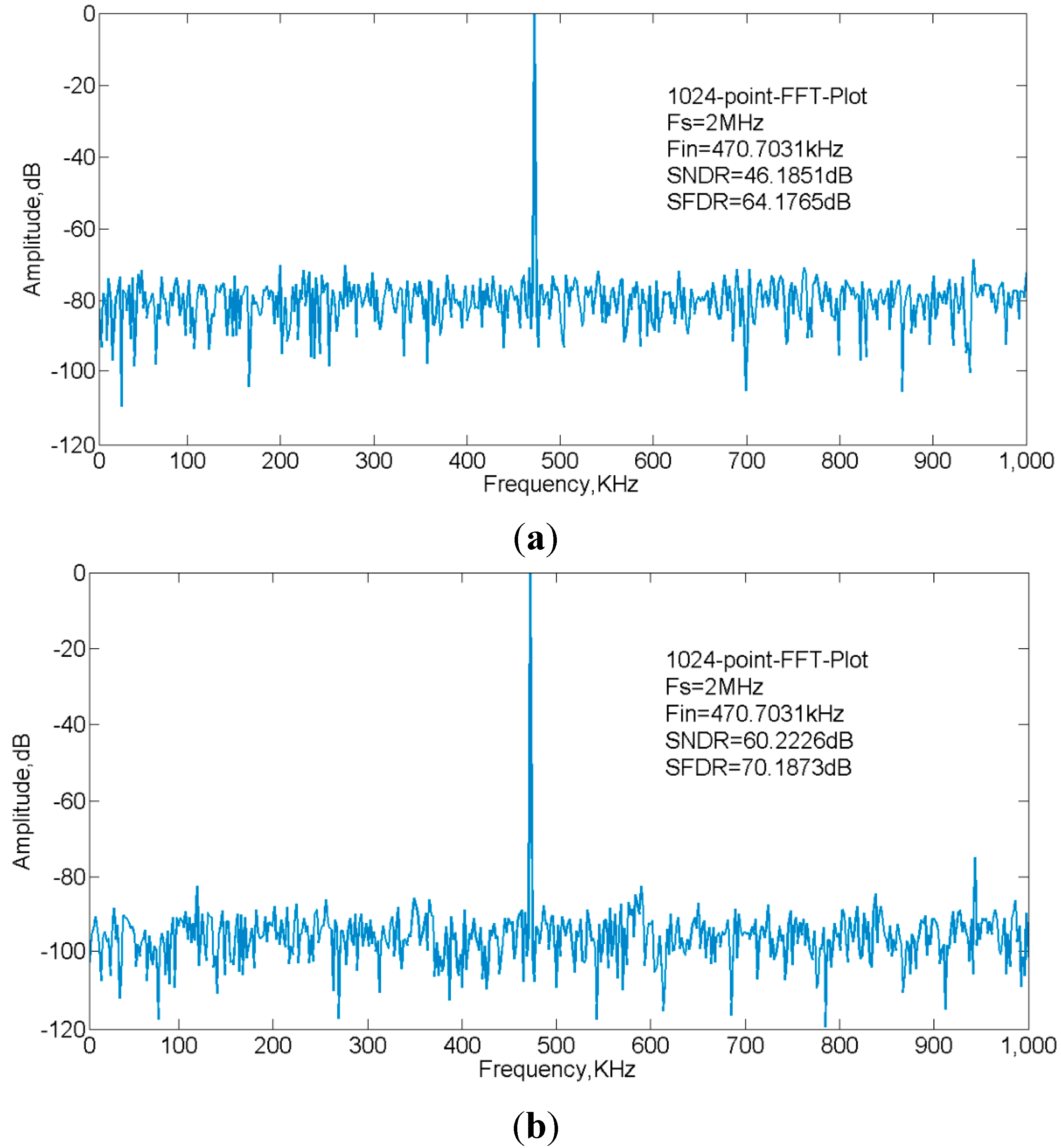
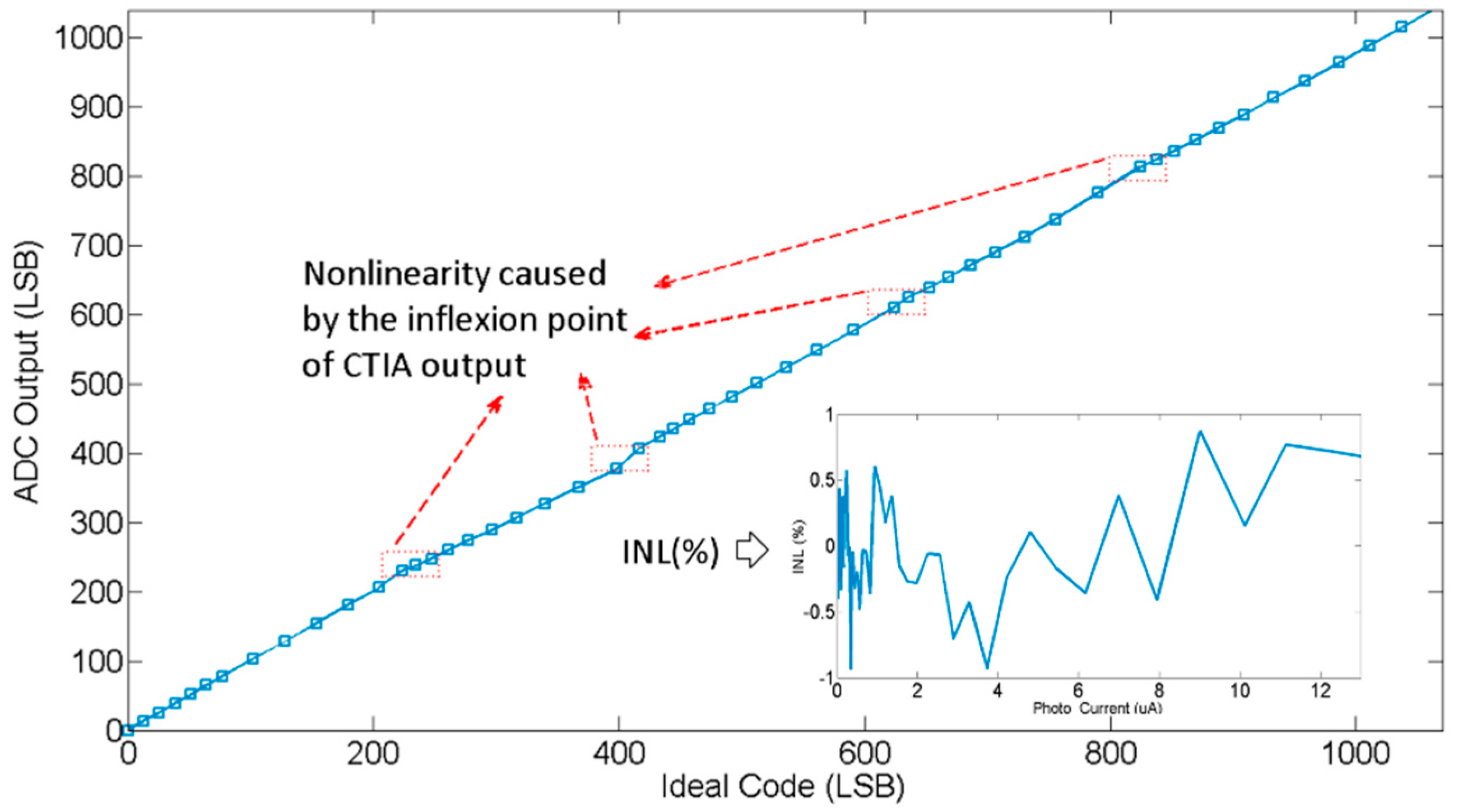
4.1. Readout Circuits

The polyline type photocurrent response curve is shown in Figure 13. As the photocurrent increases, when the output voltage exceeds the threshold voltage each time, the sensitivity gets lower. Finally, the output curve presents as a polyline with five segments as expected. Figure 13 also shows the simulation of traditional CTIA with the same input current, and the integration capacitors are 400 fF and 42 pF, respectively. When the integration capacitor is 400 fF, the CTIA saturates easily and the output signal will no longer keeps linearity with input current, and if the capacitor of 42 pF is accessed to the circuit, the sensitivity is too low to distinguish the low light signals. The transient simulation of the pixel integration readout at different photocurrent is shown in Figure 14. The glitches on the output signal is mainly caused by two reasons: (1) The PD voltage slightly deviates from VPD_RST since the OPA is not ideal, which would make a difference between PD voltage and the voltage on the left plate of capacitors; (2) When the OPA outputs large current, the negative terminal of OPA deviates from Vref, which would also generate offset between PD voltage and the voltage on the left plate of capacitors; (3) The reset noise at the left plate of additional integration capacitors make its voltage various from VPD_RST, which contributes to the glitches and noise. Noise performance is also simulated, the total noise is 0.7 mV including OPA and KT/C noise induced by capacitors and switches. Then the minimum photo current can be detected is 0.14 nA, and the non-saturated photo current is 12.5 μA. The dynamic range of this readout circuit is extended from 69.11 dB to 99.02 dB.
Figure 13. Output voltage versus photocurrent. The pixel saturates at around 12.5 μA.
Sensors 15 28224 g013
Figure 14. The transient simulation of the pixel integration.
Sensors 15 28224 g014

4.2. ADC

Different delay skews are simulated by interpolating different dummy loads and delay cells to the propagation path. Simulated quantization error in negative cases (ΔTp < 0) without calibration are illustrated in Figure 15.
Figure 15. Quantization error without calibration. (a) −Tclk < ΔTp < −Tclk/2; (b) −Tclk/2 < ΔTp < −100 ps; (c) −100ps < ΔTp < 0.
Sensors 15 28224 g015
The quantization error gets better as the delay skew gets shorter, but even in Figure 15c, i.e., when the delay skew is less than 100 ps, the quantization error still exists. The maximum deviation value is +1.78 LSB/−15.76 LSB when −100 ps < ΔTp < 0, which the following comparison is based on.
The maximum DNL and INL without calibration is +15.90/−15.36 LSB and +1.78/−15.76 LSB, which is easily obtained from the quantization error result. As shown in Figure 16, the DNL and INL drop to +0.31/−0.11 LSB and +0.25/−0.51 LSB with the proposed error correction.
Figure 16. DNL and INL with calibration.
Sensors 15 28224 g016
By applying a 470.7031 KHz sinusoid input sampled at 2 MS/s in the simulation, the 1024-point FFT spectrum shows the ADC achieves 60.22 dB SNDR and 70.18 dB SFDR after calibration while it was limited to 46.18 dB SNDR and 64.17 dB SFDR before calibration, as illustrated in Figure 17. The ENOB measured is 7.37 bit without calibration, which is close to the coarse conversion accuracy. By applying the error calibration, the maximum ENOB has been improved to 9.71 bit. As the sinusoid input frequency decreases, the improvement effect is more remarkable. The comparison of characteristics is summarized in Table 1. The ADC performance has significantly improved with the proposed calibration technique.
Table 1. Simulated result comparison.
Without CalibrationWith Calibration
SFDR(@470.7031k), SNDR(@470.7031k)64.17 dB 46.18 dB70.18 dB 60.22 dB
ENOB(@470.7031k)7.31 bit9.71 bit
SFDR(@1.9531k), SNDR(@1.9531k)49.87 dB 39.38 dB69.59 dB 60.19 dB
ENOB(@1.9531k)6.25 bit9.72 bit
DNL(max)+15.90/−15.36 LSB+0.31/−0.11 LSB
INL(max)+1.78/−15.76 LSB+0.25/−0.51 LSB
The linearity of the proposed image sensor is shown in Figure 18. The ADC output is extracted at different photo current, and the ideal code is calculated by Equation (7) at the same photo current sequence. An overall nonlinearity or INL as a function of photo current is also shown in this figure. The INL includes nonlinearity of the readout circuit and the column-ADC. The maximum INL is +0.87%/−0.91% to the full scale of linear range. As shown in Figure 18, the nonlinearity in marked region is caused by charge injection effect when different capacitors are switched to the circuit. A good linearity could be obtained in every segment if the inflexion point is ignored.
The figure of merit (FOM) is defined as the following equation:
F O M A D C = P o w e r / (2 ENOB × F S )
where Fs is 2 MS/s, thus the FOMADC of each column is 211 fJ/step. Table 2 shows the performance comparisons of various column-parallel ADCs. The proposed ADC works in time-domain instead of voltage-domain, and thus the complexity and power consumption is significantly reduced. Compared with previous works, the proposed ADC achieves high conversion speed and the best FOM.
Figure 17. ADC output spectrum. (a) Without calibration; (b) With calibration.
Sensors 15 28224 g017
Figure 18. The linearity of the proposed image sensor
Sensors 15 28224 g018
Table 2. Comparison with other types of the column-parallel ADC.
Reference[10][12][14][15][18]This Work
Technology0.18-μm0.18-μm0.18-μm0.35-μm0.25-μm0.13-μm
ArchitectureSARCyclicSingle SlopeTwo-step SSMultiple-ramp SSSS With TDC
Resolution/bit81312101010
Conversion time/μs1.26.49.54160.5
Power/μW209450 *166.7 *15091355
FOM/fJ/step983.6442.6385.9585.91138211
* Values came from full-chip power consumption.
All the sensor characteristics obtained from simulation results are listed in Table 3. The dynamic range is extended from 69.11 dB to 99.02 dB with nearly 30 dB improvement, and the ADC can effectively operate at 2 MS/s with a calibration method. Therefore, the proposed readout technique can fulfill both high speed and wide range detection features. The maximum line rate is 2 M lines/s if the ADC is implemented as column circuits. Moreover, it can be configured accordingly, e.g., the line rate could be 500 K lines/s if one ADC is shared among four columns.
Table 3. Summary of the sensor characteristics.
Technology Photodiode Size0.13 μm 1P3M 25 μm × 100 μm
Supply Voltage3.3 V/1.5 V
Line Rate 2 M
Sensitivity2.5 V/pA·s (max); 0.025 V/pA·s (min)
Noise Floor0.7 mV
Dynamic Range99.02 dB
ADC resolution10 bit
ADC ENOB9.72 bit (with calibration); 7.31 bit (without calibration)
Power Consumption1048 μW/column

5. Conclusions

A DR enhanced readout technique with two-step TDC for high speed linear CMOS image sensors is proposed in this paper. A multi-capacitor and self-regulated CTIA structure is proposed where the adjustable integration capacitors significantly extend the dynamic range. Moreover, a 10-bit column ADC based on two-step TDC with error calibration is proposed to improve the column conversion rate. The proposed ADC has a significantly increased conversion rate compared with the conventional SS ADC, and requires less power and area than the multiple-ramp ADC. The calibration method can effectively compensate the quantization error caused by the propagation delay skew within −Tclk~+Tclk without increasing the circuit complexity. Simulation results indicate that the readout circuits can achieve a dynamic range of 99.02 dB with nearly 30 dB improvement, and the ADC can achieve 9.71 bit ENOB at 2 MS/s with 355 μW power consumption. The DNL/INL are significantly reduced down to +0.31/−0.11 LSB and +0.25/−0.51 LSB with calibration. Therefore, the proposed image sensor can fulfill the high speed and wide range detection features.

Acknowledgments

Shilin Shen helped a lot in performing the simulation and revision of this manuscript. This work was supported by National Natural Science Foundation of China (61234003, 61274021).

Author Contributions

Zhiyuan Gao and Congjie Yang conceived the ideas and innovations, performed the simulation and analyzed the data; Jiangtao Xu provided supervision and guidance in this work; Kaiming Nie contributed a lot to the circuit design and layout; Zhiyuan Gao wrote the paper.

Conflicts of Interest

The authors declare no conflict of interest.

References

  1. Srikantha, A.; Sidibé, D. Ghost detection and removal for high dynamic range images: Recent advances. Signal Process. Image Commun. 2012, 27, 650–662. [Google Scholar] [CrossRef]
  2. Spivak, A.; Benlenky, A.; Fish, A.; Yadid, P.O. Wide-Dynamic-Range CMOS Image Sensors—Comparative Performance Analysis. Electron Devices IEEE Trans. 2009, 56, 2446–2461. [Google Scholar] [CrossRef]
  3. Posch, C.; Matolin, D.; Wohlgenannt, R. A QVGA 143dB dynamic range asynchronous address-event PWM dynamic image sensor with lossless pixel-level video compression. In Proceeding of the 2010 IEEE International Conference on Solid-State Circuits Conference (ISSCC), San Francisco, CA, USA, 7–11 February 2010; pp. 400–401.
  4. Kavusi, S.; Gamal, A.E. Quantitative study of high-dynamic-range image sensor architectures. Proc. SPIE 2004, 5301, 264–275. [Google Scholar]
  5. Ruan, A.W.; Shen, K.; Hu, B. Adjustable gain CTIA cell with variable integration time for IRFPA applications. In Proceeding of the International Conference on Communications, Circuits and Systems (ICCCAS), Milpitas, CA, USA, 23–25 July 2009; pp. 1066–1069.
  6. Hsieh, C.C.; Wu, C.Y.; Sun, T.P.; Jih, F.W.; Cherng, Y.T. High-Performance CMOS Buffered Gate Modulation Input (BGMI) Readout Circuits for IRFPA. IEEE J. Solid-State Circuits 1998, 33, 1188–1198. [Google Scholar] [CrossRef]
  7. Cao, Y.; Pan, X.F.; Zhao, X.J.; Wu, H.S. An Analog Gamma Correction Scheme for High Dynamic Range CMOS Logarithmic Image Sensors. Sensors 2014, 14, 24132–24145. [Google Scholar] [CrossRef] [PubMed]
  8. Inkyu, B.; Byeungseok, Y.; Kyounghoon, Y. In-pixel calibration of temperature dependent FPN for a wide dynamic-range dual-capture CMOS image sensor. In Proceeding of the IEEE International Conference on Consumer Electronics (ISCE), JeJu Island, Korea, 22–25 June 2014; pp. 1–3.
  9. Sasaki, M.; Mase, M.; Kawahito, S.; Tadokoro, Y. A wide-dynamic-range CMOS image sensor based on multiple short exposure-time readout with multiple-resolution column-parallel ADC. IEEE Sens. J. 2007, 7, 151–158. [Google Scholar] [CrossRef]
  10. Chen, D.G.; Fang, T.; Bermak, A. A Low-Power Pilot-DAC Based Column Parallel 8b SAR ADC with Forward Error Correction for CMOS Image Sensors. IEEE Trans. Circuits Syst. 2013, 60, 2572–2583. [Google Scholar] [CrossRef]
  11. Shin, M.-S.; Kwon, O.-K. 14-bit two-step successive approximation ADC with calibration circuit for high-resolution CMOS imagers. Electron. Lett. 2011, 47, 790–791. [Google Scholar] [CrossRef]
  12. Seo, M.-W.; Suh, S.-H.; Iida, T.; Takasawa, T.; Isobe, K.; Watanabe, T.; Itoh, S.; Yasutomi, K.; Kawahito, S. A low-noise high intrascene dynamic range CMOS image sensor with a 13 to 19b variable-resolution column-parallel folding-integration/cyclic ADC. Solid-State Circuits IEEE J. 2012, 47, 272–283. [Google Scholar] [CrossRef]
  13. Yeh, S.-F.; Hsieh, C.-C.; Cheng, C.-J.; Liu, C.-K. A novel single slope ADC design for wide dynamic range CMOS image sensors. In Proceeding of 2011 IEEE on Sensors, Limerick, Ireland, 28–31 October 2011; pp. 889–892.
  14. Yoshihara, S.; Nitta, Y.; Kikuchi, M.; Koseki, K.; Ito, Y.; Inada, Y.; Kuramochi, S.; Wakabayashi, H.; Okano, M.; Kuriyama, H.; et al. A 1/ l.8-ineh 6.4M Pixel 60 frames/s CMOS Image Sensor with Seamless Mode Change. IEEE J. Solid-State Circuits 2006, 41, 2998–3006. [Google Scholar] [CrossRef]
  15. Lim, S.; Lee, J.; Kim, D.; Han, G. A high-speed CMOS image sensor with column-parallel two-step single-slope ADCs. IEEE Trans. Electron Devices 2009, 56, 393–398. [Google Scholar] [CrossRef]
  16. Bae, J.; Kim, D.; Ham, S.; Chae, Y.; Song, M. A two-step a/d conversion and column self-calibration technique for low noise CMOS image sensors. Sensors 2014, 14, 11825–11843. [Google Scholar] [CrossRef] [PubMed]
  17. Lyu, T.; Yao, S.Y.; Nie, K.M.; Xu, J.T. A 12-Bit High-Speed Column-Parallel Two-Step Single-Slope ADC for CMOS Image Sensors. Sensors 2014, 14, 21603–21625. [Google Scholar] [CrossRef] [PubMed]
  18. Snoeij, M.F.; Theuwissen, A.J.P.; Makinwa, K.A.A.; Huijsing, J.H. Multiple-ramp column-parallel ADC architectures for CMOS image sensors. IEEE J. Solid-State Circuits 2007, 42, 2968–2977. [Google Scholar] [CrossRef]
  19. Muung, S.; Ikebe, M.; Motohisa, J.; Sano, E. Column parallel single-slope ADC with time to digital converter for CMOS imager. In Proceeding of the IEEE International Conference on Electronics, Circuits, and Systems (ICECS) 2010, Athens, Greece, 12–15 December 2010; pp. 863–866.
  20. Naraghi, S.; Courcy, M.; Flynn, M.P. A 9-bit, 14 μW and 0.06 mm Pulse Position Modulation ADC in 90 nm Digital CMOS. IEEE J. Solid-State Circuits 2010, 45, 1870–1880. [Google Scholar] [CrossRef]
  21. Murari, K.; Etienne-Cumimings, R.; Thakor, N.V.; Cauwenberghs, G. A CMOS In-Pixel CTIA High Sensitivity Fluorescence Imager. IEEE Trans. Biomed. Circuits Syst. 2011, 5, 449–458. [Google Scholar] [CrossRef] [PubMed]
  22. Kavusi, S.; Ghosh, K.; Abbas, E.G. Architectures for high Dynamic Range, High Speed Image Sensor Readout Circuits. In Proceeding of the International Conference on Very Large Scale Integration (VLSI), 2006 IFIP, Nice, France, 16–18 October 2006; pp. 36–41.
  23. Dudek, P.; Szczepanski, S.; Hatfield, J.V. A high-resolution CMOS time-to-digital converter utilizing a Vernier delay line. IEEE J. Solid-State Circuits 2000, 35, 240–247. [Google Scholar] [CrossRef]

