A Multi-Channel, Flex-Rigid ECoG Microelectrode Array for Visual Cortical Interfacing

Abstract
: High-density electrocortical (ECoG) microelectrode arrays are promising signal-acquisition platforms for brain-computer interfaces envisioned, e.g., as high-performance communication solutions for paralyzed persons. We propose a multi-channel microelectrode array capable of recording ECoG field potentials with high spatial resolution. The proposed array is of a 150 mm2 total recording area; it has 124 circular electrodes (100, 300 and 500 μm in diameter) situated on the edges of concentric hexagons (min. 0.8 mm interdistance) and a skull-facing reference electrode (2.5 mm2 surface area). The array is processed as a free-standing device to enable monolithic integration of a rigid interposer, designed for soldering of fine-pitch SMD-connectors on a minimal assembly area. Electrochemical characterization revealed distinct impedance spectral bands for the 100, 300 and 500 μm-type electrodes, and for the array's own reference. Epidural recordings from the primary visual cortex (V1) of an awake Rhesus macaque showed natural electrophysiological signals and clear responses to standard visual stimulation. The ECoG electrodes of larger surface area recorded signals with greater spectral power in the gamma band, while the skull-facing reference electrode provided higher average gamma power spectral density (γPSD) than the common average referencing technique.1. Introduction
Cortical electrode devices provide a deeper insight and understanding of how the brain processes information and therefore advance the performance of brain-computer interfaces (BCIs) and neuroprosthetics. In this regard, high-density electrocorticographic (ECoG) electrode arrays, capable of recording neural signals directly from the cortical surface, offer detailed information about cognitive behaviour with high speed and accuracy and therefore serve as a basis for weakly-invasive high-performance BCIs [1]. ECoG signals excel EEG in their signal quality: ECoG has higher spatial resolution (in the mm-range [2,3]) and signal-to-noise ratio [4,5]. Frequencies above 40 Hz are difficult to record in a reliable manner with EEG, while ECoG has the bandwidth to cover the broad gamma band from 40 to several hundred Hertz [6]. Both ECoG and intracortical recordings closely correlate with specific aspects of sensory-motor and cognitive function [2,7–15], as well as with the fMRI BOLD signal [16–18], and allow observation of interactions between distant cortical sites [19–21]. Although intracortical recordings can measure the neuronal activity of a single cortical cell, their functional stability is very limited over time [22–26]. For these reasons, ECoG recordings are an attractive alternative signal-acquisition method for the study of brain function and neuronal interactions, and for weakly invasive BCIs with the aim of improving the quality of life of people afflicted by neurological disorders [27–37].
Clinical ECoG applications include the localization of epileptic seizures, intraoperative functional mapping and assessment of the limits of resection. Typically, these electrodes are of 1 to 2.3 mm diameter and 10 mm inter-electrode distance, embedded in a 0.4–0.6 mm-thick Silastic® base [23,38]. Smaller-area electrode arrays, for dedicated research in humans, are implanted together with the larger ones, and these have electrodes of 70–1500 μm diameter and 1–4 mm inter-electrode distance [39,40].
Current ECoG microelectrode arrays used in research are highly flexible [41] and only several microns thick; they have also reached much higher electrode count: up to 252 [42] and 360 [43], with typical electrode diameters ranging from 300 to 1000 μm. The effect of electrode size on the coherence of ECoG signals has already been studied, but only with electrodes larger than 1mm and for inter-electrode distances greater than 1 mm [44,45]. Therefore we aimed to provide an electrode array with electrodes of different size in close neighbourhood that will allow for future investigations on the effects of electrode size in the sub-millimetre range. The highly flexible nature of these ECoG microelectrode arrays has required non-conventional assembly techniques for electrical connectors such as zero-insertion-force (ZIF) connectors [46–49]; anisotropic conductive film (ACF), applied between the pad-end and a fan-out PCB [43,50–53]; soldering of through-hole connectors directly to an ultra-flexible platform [42,54,55]; and isotropic conductive epoxy [56–58]. Each of these solutions can be advantageous within a certain range of electrode count and array application. High-electrode count ECoG arrays for applications on freely-moving animals call for miniature connectors, preferably fine-pitch and densely packed ones. The connector-assembly on these highly flexible devices can turn into a challenging task. A perfectly flat and rigid platform could solve this problem, provided it is monolithically integrated into the fabrication flow of the highly flexible device. Inspired by the F2R approach for the assembly of microsensors onto catheters [59], we made first advances toward a highly flexible ECoG array containing a rigid assembly platform [60,61]. In this paper we propose a finalized fabrication and assembly flow for a multi-channel ECoG microelectrode array, which bears a flat and rigid platform, cast out of the substrate wafer during microfabrication. We investigated the reliability of the assembly platform with electrical tests. Furthermore, we characterized the array electrodes (100, 300 and 500 μm in diameters) by means of electrochemical impedance spectroscopy and measured the effect of electrode size on impedance magnitude and phase. Finally, we demonstrated that the array worked in vivo via epidural recordings from the visual cortex of an awake Rhesus macaque. We showed its usability for investigating effects of electrode size on the recorded ECoG signals and for comparing the influence of a skull-facing reference electrode with a common average reference signal.
2. Materials and Methods
2.1. Array Design
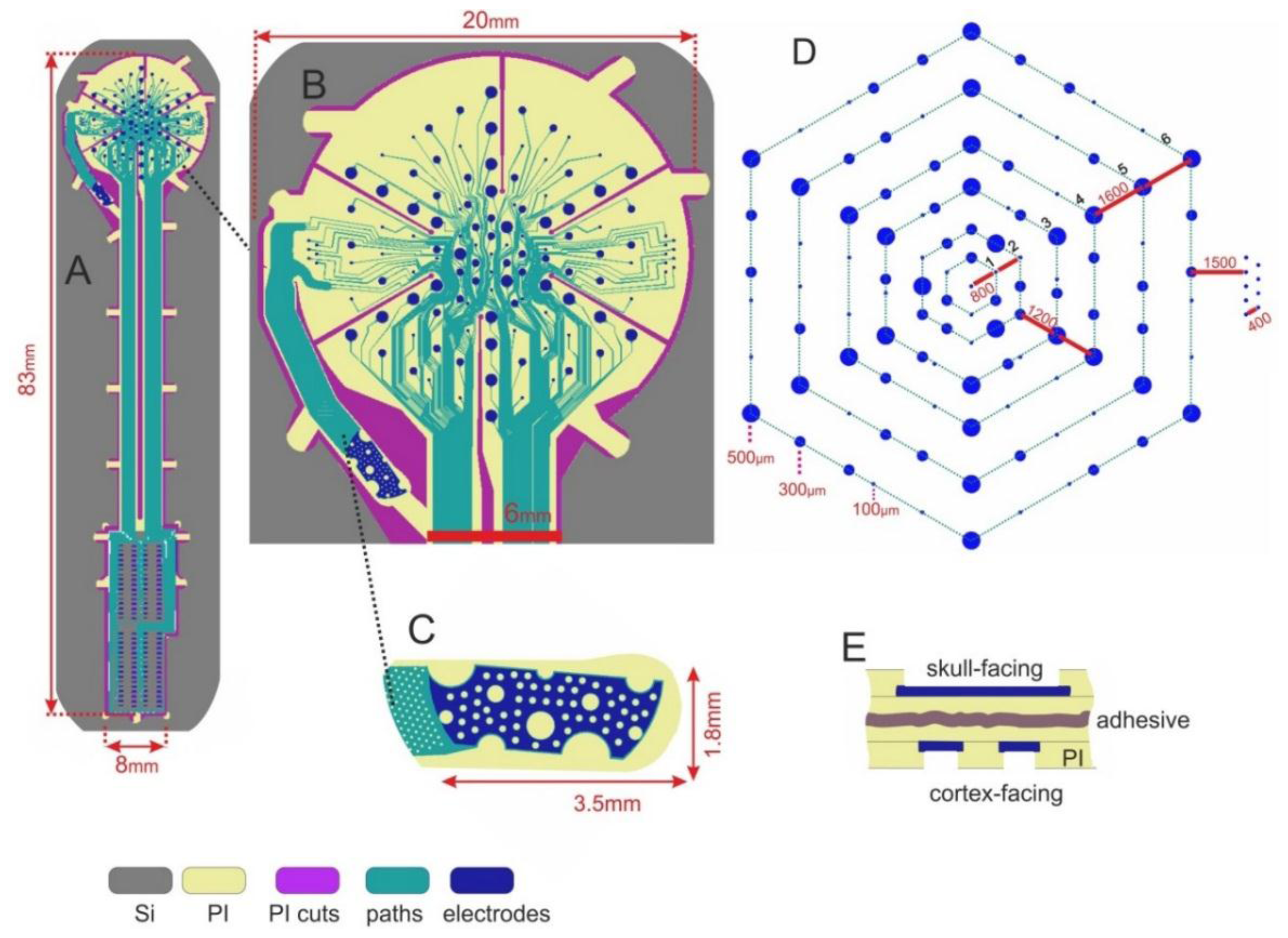
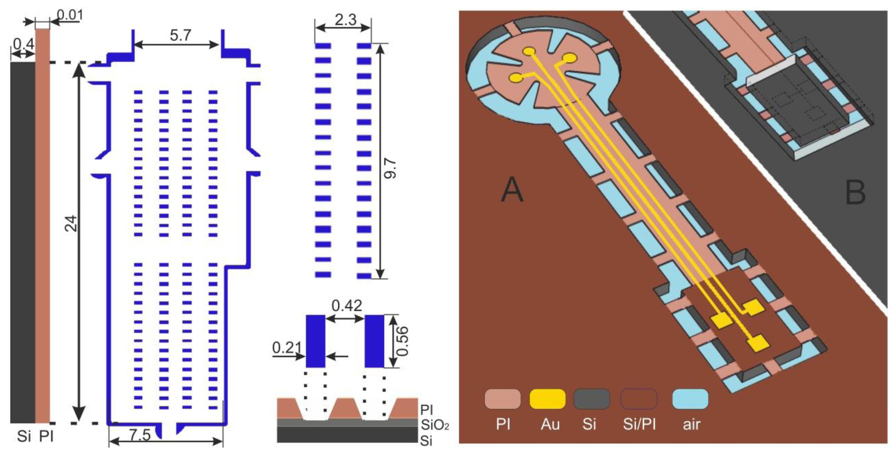
The layout of the proposed ECoG electrode array is shown in Figure 1A: its electrodes are enclosed by a circular area, connected by a straight cable to a rectangular assembly region. The electrode and cable regions were designed to be embedded in polyimide (PI), while the assembly portion was to be made out of silicon (Si). The ECoG signal-acquisition area (Figure 1B) contains 124 circular electrodes of three different sizes and a much larger reference electrode, situated beside the array. Conduction lines (15 μm wide) connect the electrodes to the assembly region where the output connectors are to be placed. Most connection lines are forced to pass through the centre of the array at a 15 μm inter-line distance in order to allow several radial cuts. These radial cuts perforate the flexible material of the array so that upon implantation it can conform to the curved shape of the brain surface without formation of folds. Beside the radial cuts there are curvilinear cuts which define the edges of the array, the outlines of its reference electrode and the borders of several flexible straps, which will mechanically fix the array to its carrier wafer in the final fabrication step. A detailed view of the ECoG electrode arrangement is shown in Figure 1D. Circular electrodes (109 in total) are designed in three different sizes (100, 300 and 500 μm in diameter), allowing to investigate how electrode size affects signal characteristics and, at a later stage, the features of stimulus-induced and stimulus-evoked field potentials. They are situated on a set of concentric hexagons and span the ECoG signal-acquisition area. Additionally, two sets of electrodes (100 μm in diameter) are arranged in groups outside the outermost hexagon, intended for high-resolution spatial frequency test measurements. The reference electrode, shown separately in Figure 1C, has a surface area of 2.5 mm2, and it is orders of magnitude larger than any other single ECoG electrode to ensure high signal-to-noise ratio. After completion of all manufacturing steps all flexible straps are cut through to release the ECoG device from its carrier wafer; the reference electrode is bent to the backside of the array, thus facing the skull during in vivo recordings (see Figure 1E). Holes of different sizes were designed in the reference electrode (1) to prevent crack formation in the metal film and (2) to minimize parasitic capacitive coupling since the hole-pattern of the reference electrode is a mirror image of the underlying electrode pattern. A detailed view of the connector-assembly region is presented in Figure 2, left image. Its 200 mm2 surface area is intended for the assembly of four 32-pin SMD-connectors. Each soldering pad has 210 μm × 560 μm area. The distance between two adjacent pads is 420 μm. The area of the connector- assembly region is 24 mm × 7.5 mm; the thickness of the silicon interposer is 400 μm.
Usually, ECoG electrode arrays are fabricated by spin-coating a flexible stack on a substrate wafer, which is peeled from the substrate in the final step to become a thin flexible device. In order to realize a rigid platform which is monolithically integrated in the microfabrication process of a flexible device, the substrate can instead come into use. By processing the backside of the carrier wafer, the substrate beneath the ECoG electrodes/cable is fully removed, while a silicon rectangle is cast out beneath the assembly area. In this manner, a free-standing flex-rigid device is realized as shown in Figure 2, right image: top side in A and backside in B.
2.2. Microfabrication
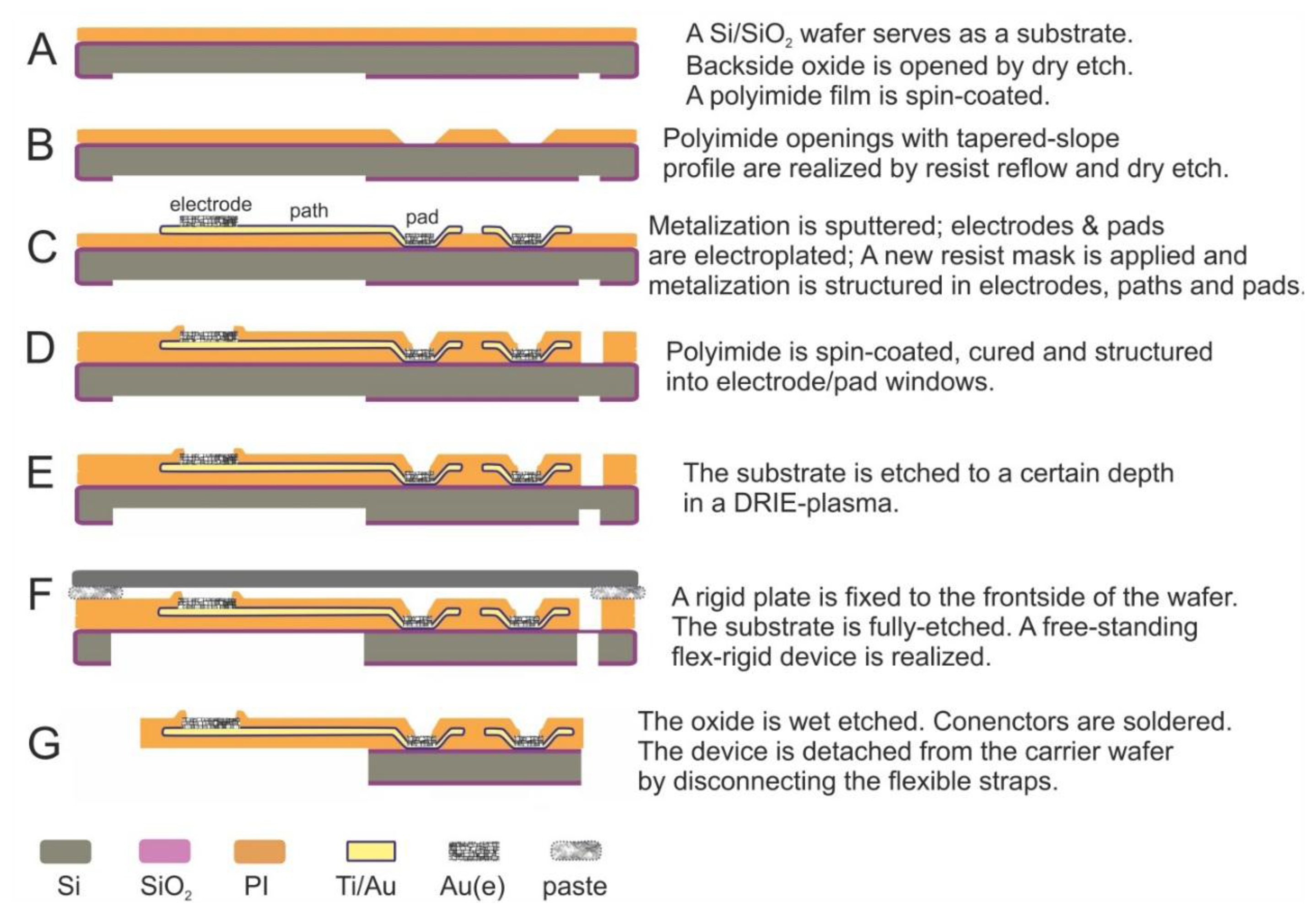
The fabrication of the free-standing flex-rigid device is presented in Figure 3. A 750 nm-thick thermal oxide is grown on a silicon wafer (4″, 380 μm thick). A photoresist mask, defining the array's flexible and rigid regions, is realized on the wafer backside (1.8 μm-thick AZ1518 photoresist; MA6 mask aligner, Süss, Garching, Germany; AZ726MIF developer, MicroChemicals, Ulm, Germany). The mask is transferred into the oxide beneath by dry etching (CF4-RIE plasma, ALCATEL 601E, ALCATEL, Annecy, France). The resist is stripped in AZ100 and the wafer is cleaned. Next, the wafer front side is spin-coated with VM651 organosilane adhesion promoter, followed by spin-coating of U-Varnish polyimide film at 3000 rpm for 40 s. The polyimide is soft-baked on a hotplate (5 min@80–120 °C & 5 min@120 °C) and then cured in a N2-atmosphere (10 min@450 °C peak), resulting in a final polyimide thickness of 5 μm. In this way, the backside oxide is structured into array outlines of flexible/rigid regions and then the first polyimide layer is realized on the wafer front-side (Figure 3A).
In the next stage, the wafer is cleaned by IPA, water-rinsed and dried. The polyimide surface is activated in O2 plasma to promote a good photoresist adhesion. A photoresist is spin-coated and structured into rectangular windows (10 μm-thick AZ9260 resist). The photoresist is then thermally reflowed to obtain a smooth step profile (1 h@120 °C). Then, the step profile of the reflowed resist is transferred in polyimide (RIE-plasma, STS ICP tool). The resist is stripped in AZ100. Hence, rectangular windows with a tapered slope are realized in polyimide; these windows define the regions where soldering pads will be situated (Figure 3B).
Next, the polyimide is dried, its surface is treated in O2 plasma and a 20 nm/300 nm-tick Ti/Au metallization stack is sputtered onto the polyimide. A photoresist film is applied and structured into electrode and pad windows (O2 plasma surface activation, 1.8 μm-thick AZ1518) and a 2.5 μm-thick gold layer is deposited via electroplating onto the windows. The photoresist is removed in AZ100. Another 1.8 μm-thick AZ1518 photoresist is spin-coated and structured into electrodes, paths and pads. The resist mask is transferred into the Au film (3–4 min in NaCN) and subsequently in Ti (30 s in BOE). The photoresist is stripped in AZ100. ECoG electrodes on polyimide and Ti/Au pads on Si/SiO2 are realized in this way (Figure 3C). The heat and O2 plasma treatment directly before metal sputtering on the polyimide layer should promote the adhesion between metal and polyimide.
In the following stage, VM651 organosilane adhesion promoter is applied and U-Varnish polyimide film is spin-coated, soft-baked and cured. A 10 μm-thick AZ9260 photoresist is spin-coated and structured into the arrays' outlines and cuts. This mask is transferred into polyimide in an O2 + CF4 RIE plasma and the photoresist is eventually stripped in AZ100. Another 10 μm-thick AZ9260 photoresist is applied, this time being structured as electrode and pad windows. These windows are then transferred in polyimide and the resist is stripped as described above. Hence, the array electrodes and pads are opened and the array outlines/cuts/straps are defined (Figures 1B and 3D). We structured the outlines/cuts/straps separately from the opening of electrodes/pads because of their different thicknesses: 10 μm and 5 μm, respectively.
In the final step, a 10 μm-thick AZ9260 photoresist is applied on the wafer backside. It is structured into a relatively large window defining the flexible area of the array and narrow lines surrounding the assembly area. The Si wafer is pre-etched on the backside to a 300 μm depth (80 min in SF6 + C4F8 DRIE plasma, STS ICP tool). The wafer is unloaded and an additional blank 4″ silicon wafer is fixed on its front side with a silicone paste (WLP 035, Fischer Elektronik, Lüdenscheid, Germany). The blank wafer serves as a mechanical stabilization platform, while the thermal-conductive paste provides a heat sink. The remaining Si is etched in ca. 40 min (Figure 3F), the blank wafer is detached and the paste is removed. The remaining oxide is then wet etched in BOE and the array wafer is rinsed and dried. In this way, a free-standing flexible electrode array with a monolithically integrated rigid interposer is fabricated. The array can be easily removed from its carrier wafer upon cutting the flexible straps (Figure 3G), which mechanically fix the array to its substrate.
2.3. Connector Assembly
The array's surface is activated in O2 plasma. A Sn-58Bi solder paste, with an 139 °C eutecticum and 20–38 μm solder powder size (LFM 65W, Almit GmbH, Michelstadt, Germany), is manually dispensed on the 128 array pads with a dispensing tip (250 μm inner-diameter) using a fluid dispenser under pressure (Nordson EFD, 1000 DVE). Four 32-pin SMD-type fine-pitch connectors (Omnetics, Nano Strip Series, NPD type, A71350-001, Omnetics Connector Corporation, Minneapolis, MN, USA) are aligned and mounted onto the pads, using a multi-purpose die bonder (FINEPLACER® pico ma, Finetech GmbH & Co., KG, Berlin, Germany). The Omnetics connectors are picked by a vacuum holder, aligned to the array pads by the overlay vision alignment system (beam splitter) and then placed onto the pads by a lever arm. A 5 mm thick Al block is used as a placeholder between the FINEPLACER hotplate and the interposer in order to focus the heat primarily to the assembly platform and to reduce the heat transfer to the fully flexible electrode regions. The soldering heat-profile consists of the following plateaus: 40 s@100 °C, 40 s@129 °C, 30 s@140 s and 20 s@165 °C, whereas the temperature refers to the connector-assembly surface. After soldering the flux residues are rinsed (Flux Remover, followed by IPA) and adhesives are applied around the connectors and interposer to ensure mechanical stability (UHU plus endfest 300, UHU GmbH, Bühl (Baden), Germany; followed by UV-cured DELO-KATIOBOND GE-680, DELO Industrie Klebstoffe, Windach, Germany). The ECoG array is released from its carrier wafer by manually cutting the polyimide straps using a scalpel.
2.4. Array Characterization
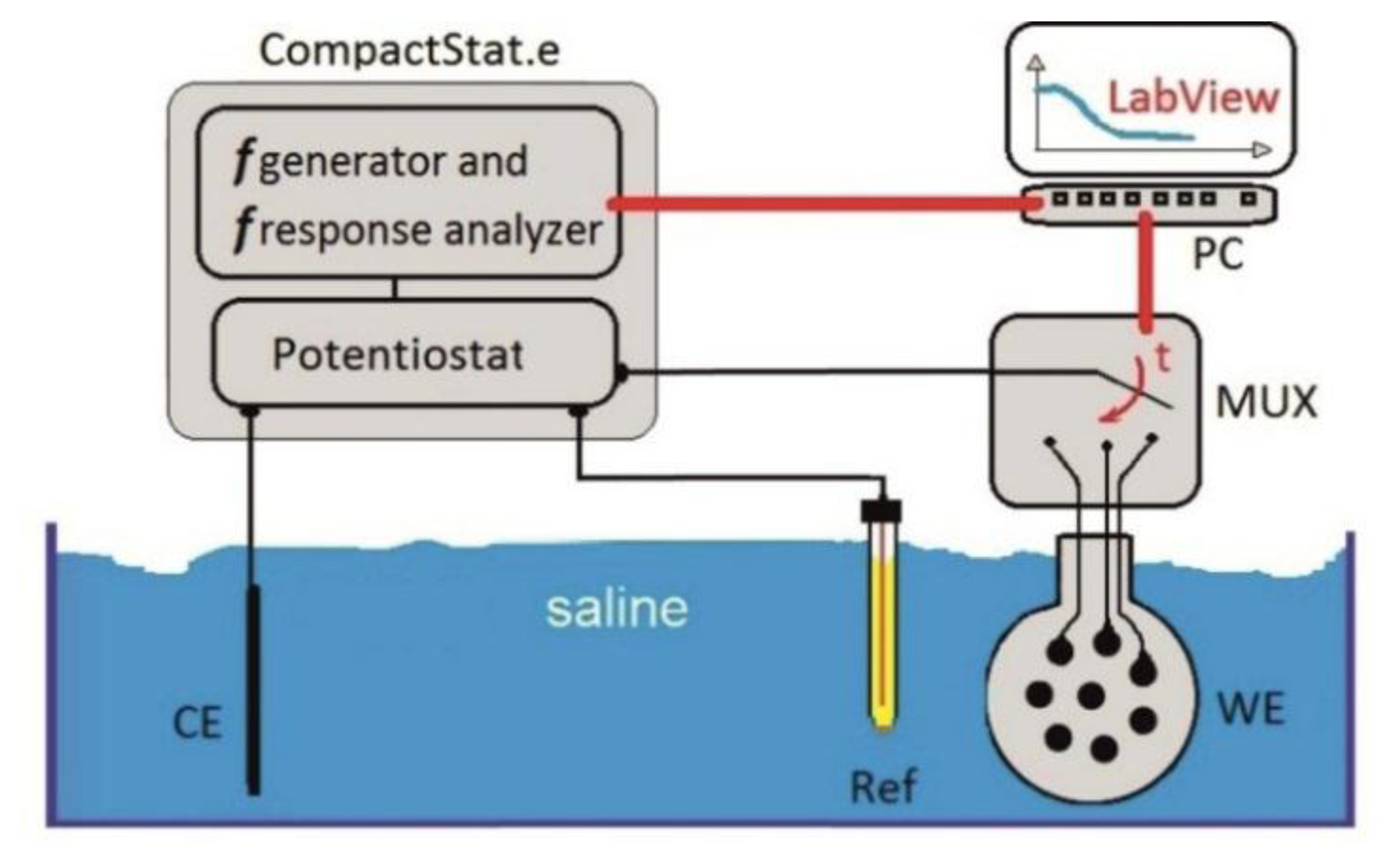
The array was characterized by performing electrochemical impedance spectroscopy (EIS) in 0.9% saline on its 128 electrodes as shown in Figure 4. The electrodes were contacted via the four 32-pin Omnetics connectors of the array. A 2 cm2 Pt electrode served as counter electrode (CE) and an Ag/AgCl electrode (Ref) was the external reference (SensorTechnik Meinsberg GmbH, Meinsberg, Germany). A 10 mV sinus was applied at the Pt-electrode, while the frequency was swept from 105 to 1 Hz. The electrode impedances were measured by a portable CompactStat.e impedance analyzer (IVIUM Technologies B.V., Eindhoven, The Netherlands). The switching between the electrode channels was performed by a NI-PXI 2530 multiplexer from National Instruments. An in-house developed LabView program provided the communication between the PXI and the CompactStat.
2.5. Implantation
All procedures and animal care were performed in accordance with the regulation for the welfare of experimental animals issued by the Federal Republic of Germany and were performed with the approval of the local authorities.
A six years old male rhesus monkey (Macaca mulatta), underwent implantation surgery in aseptic conditions. General anaesthesia was induced with ketamine/medetomidine (4 mg/kg/0.04 mg/kg injected intramuscularly) and maintained after intubation by ventilation with 30% O2–70% N2O air mixture plus 1.0% isoflurane, supplemented with fentanyl (3 μg/kg/h, intravenously). Atropine (0.05 mg/kg) was used to reduce salivation.
The ECoG array was implanted epidurally over the primary visual cortex (V1) on the brain's left hemisphere, covering the cortical map of the lower right quadrant of the visual field, between 1 and 5 degrees of eccentricity. We chose V1 because it is sufficiently large for our array to cover the representation of a lower quadrant of the visual field up to 5–6° in which our stimuli would be placed while also avoiding the centre of the visual field representation (fovea), where minimal eye movements would result in particular large shifts of activated regions. Localization of V1 in stereotactic coordinates was supported by anatomical MRI scans performed beforehand. A craniotomy of approximately 1.5 × 1.5 cm was performed using a piezo-surgery instrument (Piezosurgery®, mectron Deutschland Vertriebs GmbH, Köln, Germany), and the resulting boneflap was later refastened to the skull with a titanium stripe and screws. The cleft between the boneflap and the skull was sealed with calcium phosphate bone substitute (Norian™ CRS™ Fast Set Putty™, Norian Corporation, West Chester, PA, USA).
The connector-platform of our ECoG array was fixed to the surface of the acrylic cap with epoxy glue (Loctite 3090, Henkel, Düsseldorf, Germany). The connectors were protected from humidity and mechanical strain by a custom-made titanium chamber with an aluminium lid (NAN Instruments Ltd., Nazareth, Israel). The whole arrangement was fixed to the animal's head with dental acrylic (Palamed and Paladur, Heraeus Kulzer, Hanau, Germany) and titanium screws (Synthes GmbH, Solothurn, Switzerland) over a basic layer of UV-sensitive ceramic cement (Solid Bond P/S and Charisma Flow, Heraeus Kulzer).
2.6. Demonstration of Functioning in Vivo
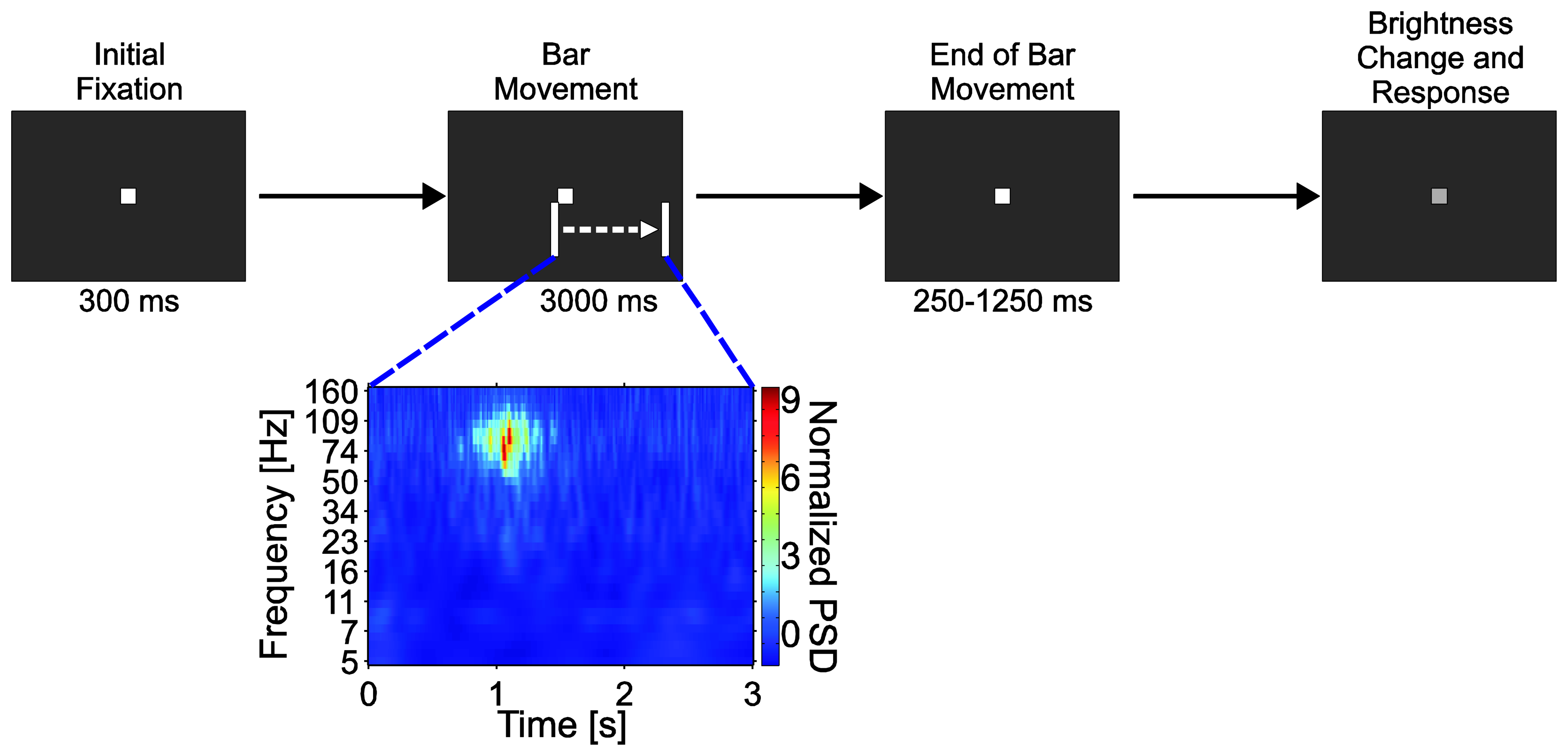
Before array implantation, the animal was trained to maintain fixation on a small bright square on the centre of a 22-inch cathode ray tube display (100 Hz, 1152 × 864 [1024 × 768], NEC MultiSync FP1355, Tokyo, Japan) over a dark background, while ignoring any other stimulus in the screen. The distance between the screen and the monkey's eyes was 86 cm, and the animal sat on a custom-made primate chair with its head fixed in space. After an initial fixation period, a bright white bar (100 mm × 3 mm; 6.7° × 0.2° visual angle) moved in a direction perpendicular to its long axis across the lower right visual field (Figure 5). Twelve equiangular directions (0°–330°) corresponding to six different bar orientations were used in the experiment. The bars moved for three seconds with constant speed of 50 mm/s (3.33°/s). Upon the end of movement, the bar stimulus disappeared, followed by a variable interval (250–1250 ms) in which no stimulus besides the fixation point was present. Finally, the monkey had to respond to a small change in the brightness of the central fixation spot to receive a liquid reward. If the animal broke fixation (fixation window diameter 1.3°, centred on the fixation point) or responded too early or too late, the trial was aborted without reward.
The four Omnetics array connectors sent the raw signals via 3-inch cables (A71273-001, Omnetics Connector Corporation) to an adaptor board that interfaced the array to the recording system. Four 32-channel headstage preamplifiers (MPA32I, Multichannel Systems MCS GmbH, Reutlingen, Germany) amplified the ECoG signals ten times. Two 32-channel signal collectors (SC2 × 32, Multichannel Systems MCS GmbH, Reutlingen, Germany) fed the signals into programmable gain amplifiers (PGA64, Multichannel Systems MCS GmbH), with a gain of 100 for all channels. The amplified signals were then sent to the data acquisition system (USB-ME256, Multichannel Systems MCS GmbH). Signals were digitized at a sample rate of 25 kHz. In addition to the signals from the array electrodes, we recorded eye position information (ISCAN Incorporated, Woburn, MA, USA) and digital information about the timing of stimuli and task events. In-vivo data were acquired between one and three months after implantation. A recording session was used for the analysis only if every single stimulus was successfully presented at least ten times. A total of 525 successful trials recorded in eight sessions were used in the subsequent analyses.
Using custom routines developed in MATLAB® (The Mathworks, Inc., Natick, MA, USA), the recorded data was filtered (direct-form FIR filter, order 422) between 1–150 Hz (gain 1, −3 dB at approx. 170 Hz) and down-sampled to 1 kHz. Forward and backward filtering was applied to avoid unwanted phase shifting. To analyse the ECoG signals in the time-frequency domain, the recorded data underwent wavelet transformation using complex Morlet wavelets with Gaussian shape in both time and frequency domains [10]. Power spectral density values (PSD) were calculated as the square of the absolute value of the wavelet-transformation divided by the Nyquist frequency (500 Hz). To build time-frequency plots of mean power spectral density, corresponding time-frequency bins of trials sharing the same stimulus were averaged and then normalized against the baseline taken from the initial fixation period of 300 ms before bar stimulus onset.
3. Results
3.1. Microfabrication
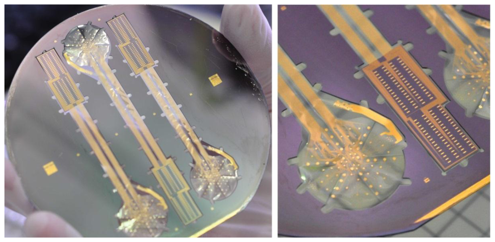
A fully processed wafer is shown in Figure 6. It contains three flex-rigid free-standing ECoG devices, spanned to the wafer by flexible straps; the signal-acquisition areas are highly flexible whereas the connector-assembly islands are rigid.
Figure 7 shows a magnification of a signal-acquisition area: 124 circular electrodes and the reference electrode placed beside them, which is connected to four separate metal paths. Hence, each of the four connectors has a separate connection path to the reference electrode.
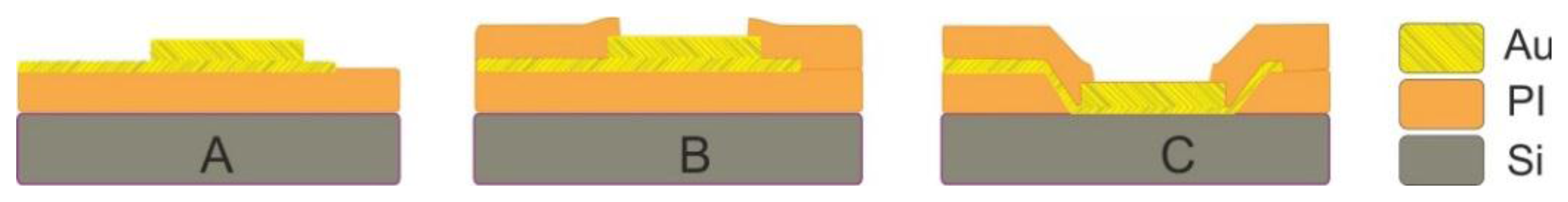
A top view of a soldering pad is presented in Figure 8A: it has a soldering area (polyimide opening) of 520 × 160 μm2 = 0.083 mm2; its metal area is slightly larger (30 μm wider on all sides) to prevent solder paste from diffusing into the metal paths. Figure 8B shows a magnification of the soldering pad: a 300 nm-thick metal path runs from left to right and splits into three sub-lines. These sub-lines run over the polyimide step (1), then over a Si/SiO2 region and enter a rectangular 2 μm-thick soldering pad (2); a top polyimide fully covers the metal paths and encircles the metal pad area (3). The sub-lines were designed to ensure that if one line breaks, there will be two others in reserve; the spacing between the lines was introduced because top PI adheres more strongly to the bottom PI than to Au.
Figure 8C shows the cross-section of a reflowed photoresist mask, whose profile was transferred into polyimide. The PI step has a slope of 20°, which can provide a smooth transition for a metallization film from the polyimide surface to the silicon substrate underneath. In this image the polyimide was etched only half-way to determine its slope angle and etch rate; in the final fabrication flow the PI is fully removed.
3.2. Connector Assembly
The connector-assembly process is presented in Figure 9. The dispensing of solder paste was performed in a slightly off-pad fashion to ease the following connector alignment (A); alignment and positioning of Omnetics connections on the solder-paste-covered pads was performed with a FINEPLACER tool. Applying the corresponding soldering heat-profile transformed the solder-paste spheres into solder-joints (B); four Omnetics connectors were soldered per array and the flux residues were cleaned (C); a packaged ECoG array with a fully encapsulated connector-assembly region can be seen in Figure 10A. Prior to implantation the bottom end of the reference electrode was flipped to the array backside and fixed by a biocompatible, high-temperature and moisture-resistant adhesive (Polytec EP653, Polytec PT GmbH, Waldbronn, Germany) to realize a skull-facing reference (Figure 10B).
3.3. Solder-Joint Characterization
The quality of solder-joints between pads and connector legs (Figure 9B) was investigated by means of electrical tests. For the electrical characterization we prepared two types of array specimen. The first type contained fully rigid soldering pads (see Figure 11C) fabricated according to Section 2.2. The second type was fabricated with state-of-the-art ECoG array pads containing PI under the metal layer (see Figure 11B), deliberately skipping fabrication step B in Figure 3. Omnetics connectors (four 32-pin connectors per specimen type) were soldered to each specimen and packaged in epoxy glue (see Section 2.3). The electrical characterization included short- and open-connection tests. During the short-connection test the dry inter-electrode dc resistance was measured with a conventional electronic multimeter in the 200 MΩ range: it revealed no parasitic short-connections. The open-connection test was performed in saline (see Section 2.4): a high number of malfunctioning solder-joints in B-type specimens were counted (15–27 open connections per 32-pin connector), whereas the C-type provided much more reliable solder-joints (0–3 open connections per 32-pin connector).
Additionally, we tested the adhesion of the Ti/Au metal pads to the underlying substrate of three specimen types (two samples à 32-pads per type) as shown in Figure 11: (A) metal pads on PI; (B) metal pads on PI which had experienced high thermal stress (curing of second PI layer for 10 min@ 450 °C); (C) metal pads on Si/SiO2 which had also undergone the same thermal stress. Scotch-tape adhesion tests [62] were performed as follows: an adhesive tape was applied on the metal pad surface; the tape tail was folded at 180° and pulled off quickly; the adhesion was considered satisfactory if no metal material was removed from the pad area. These adhesion tests revealed that the metal-PI adhesion is satisfactory if the samples do not undergo a second PI curing (specimen A); the metal-PI adhesion degrades after the second curing (specimen B), whereas metal-Si/SiO2 adhesion remains stable even after the second PI-curing (specimen C).
3.4. Electrode Characterization in Saline
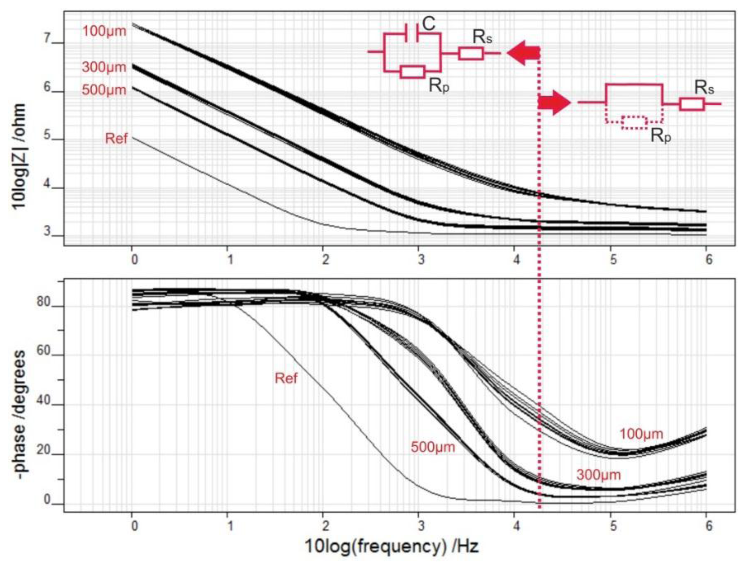
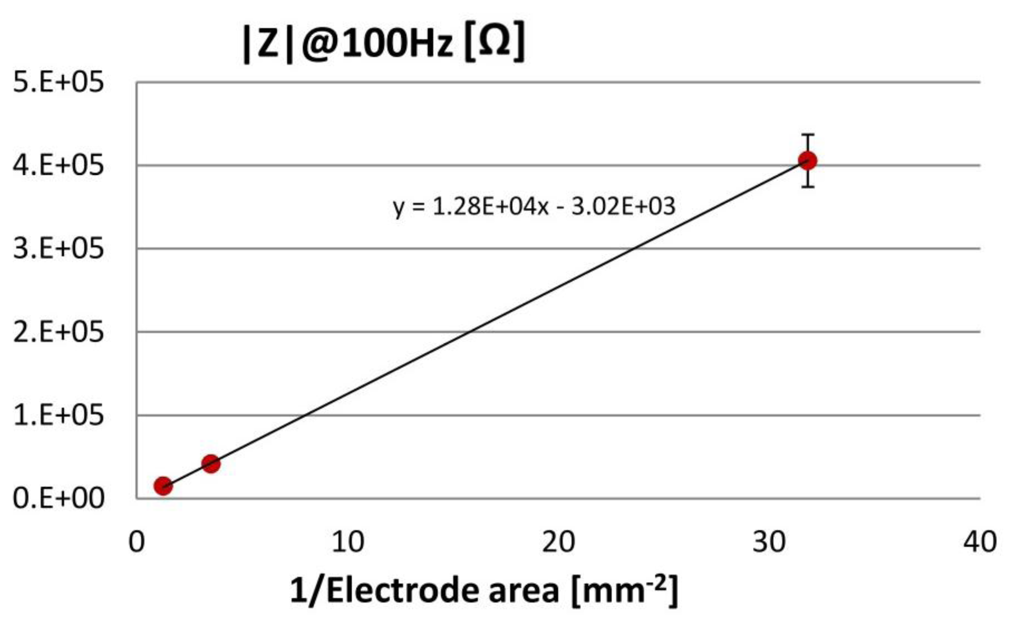
ECoG electrode arrays with fully rigid soldering pads (Figure 11C) were characterized by electrochemical impedance spectroscopy. The impedance spectral bands (magnitude and phase) were measured for each electrode type, all belonging to a common Omnetics connector (see Figure 12): the impedance magnitudes |Z| decrease with rising frequency, show capacitive behaviour in the low frequency range and resistive behaviour above 10 kHz. At 100 Hz, a frequency value associated with gamma ECoG activity, the average |Z| values are plotted in Figure 13 and they are inversely proportional to the surface areas of the 100, 300 and 500 μm-diameter electrodes.
Additionally, the impedance magnitude of the reference electrode at 100 Hz is eight times smaller than the impedance magnitude of the largest circular electrodes (500 μm-type).
The impedance of an electrode immersed in electrolyte can be modelled by an equivalent electric circuit Xc‖Rp+Rs, with Xc being a capacitive reactance, both Rp and Rs ohmic resistances [63]. As the metal electrode is negatively charged with respect to electrolyte solution, a double layer is formed at the electrode-electrolyte interface, which resembles a charged capacitor. Its capacitance C is related to Xc by the angular frequency ω: C = (ωXc)−1. Additionally, as current passes via the electrode-electrolyte interface, the resistance Rp accounts for the associated charge transfer, whereas Rs sums up the electrolyte and array-path resistances [63].
Applying the above electric circuit model to the impedance data reveals that in the low frequency range C and Rp determine the steady impedance increase at frequencies; Rs accounts for the low ohmic behaviour above 10 kHz because C shunts Rp (see Figure 12, circuit diagrams). Furthermore, the impedance data of the ECoG array were fitted using IviumSoft Electrochemistry Software (Ivium Technologies B.V., The Netherlands) to derive the C, Rp and Rs values (mean + s.e.m.). As presented in Table 1 and Figure 14, Rs belongs to the low kΩ-range; Rp spans the 1–80 MΩ-range, and it rises linearly with decreasing electrode area; C is in the 1–36 nF range and increases linearly with electrode area.
3.5. Demonstration of Functioning in Vivo
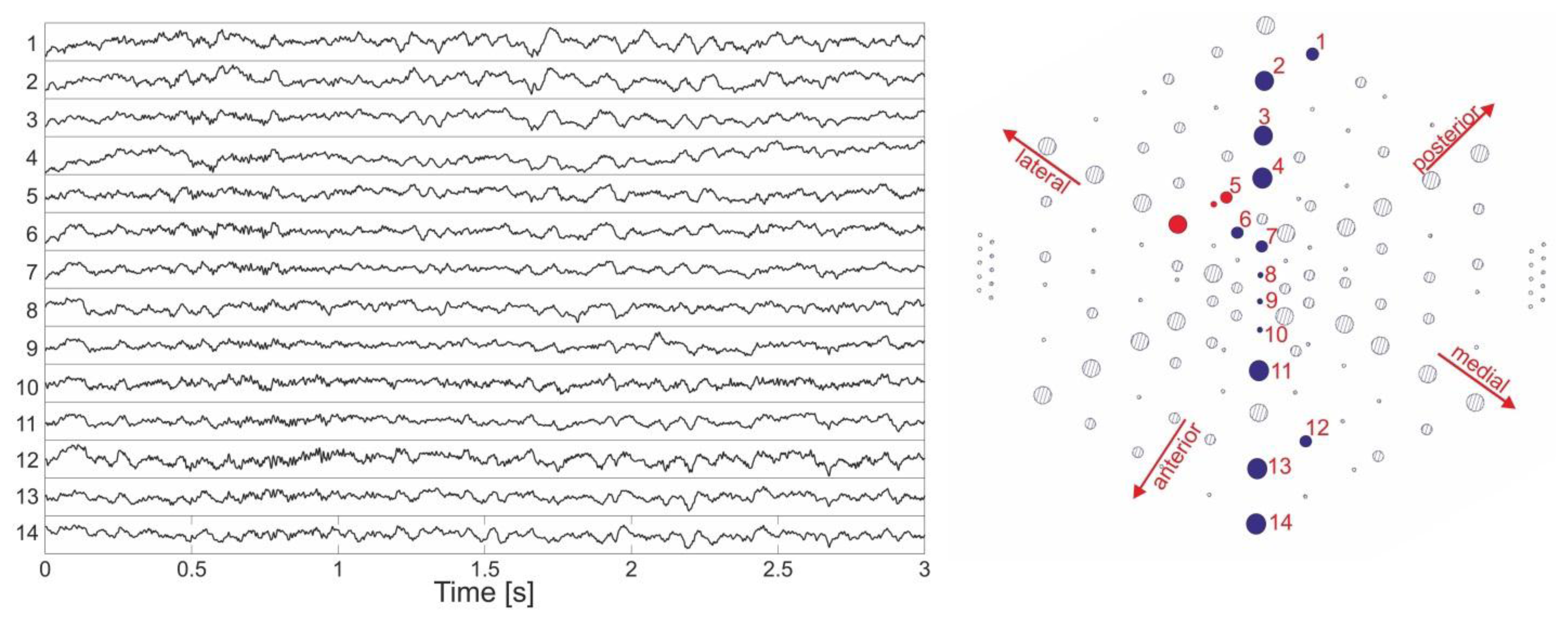
The functioning of the ECoG electrode array was demonstrated in vivo while a Rhesus monkey performed a visual fixation task, and at the same time ignored bright bars moving across the bottom-right visual quadrant of a dark screen (see Section 2.6). Figure 15 shows example traces recorded from primary visual cortex (V1) of an animal six weeks after implantation. These signals were acquired during a 3 s-long instance of bar movement (left image) from 14 ECoG electrodes spanning the arrays' diameter (#1–14, Figure 15, right image). Distinct responses in the form of faster oscillations of the electrocorticographic signal were induced by the moving bar within the first second of stimulus presentation. Electrodes situated in proximity to each other clearly showed similar oscillatory responses at approximately the same time, while those of more distant electrodes occurred in more distinct epochs as expected because of V1's retinotopic visual field map. This further confirmed that changes in the ECoG signal corresponded to a response to the moving stimulus activating successively neighbouring regions of area V1.
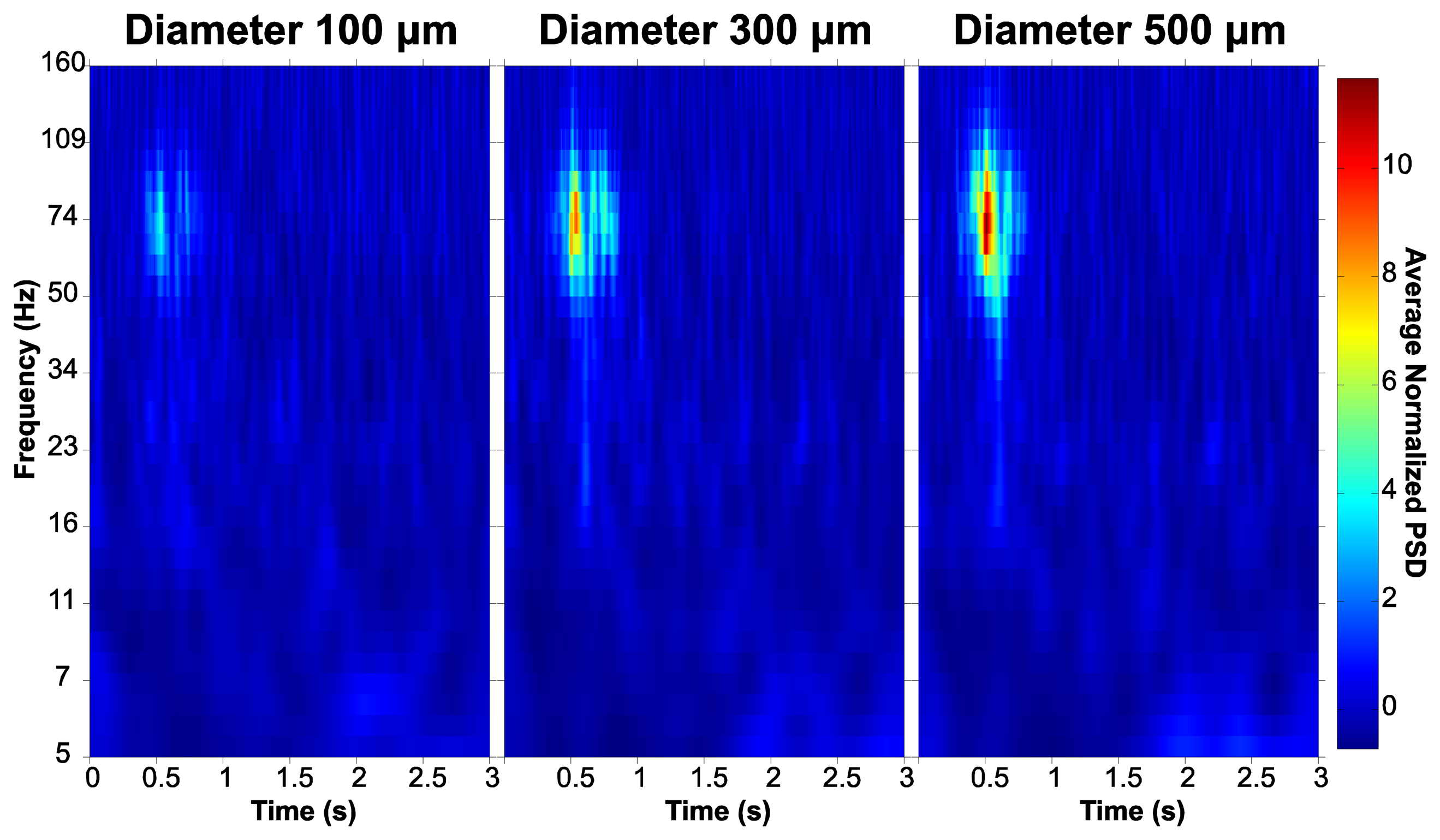
Figure 16 presents time-frequency plots of normalized power spectral density (PSD) from three neighbouring electrodes of different sizes (red dots in Figure 15). The data were averaged over all trials within a session presenting a specific moving bar stimulus (direction 300°), with stimulus onset at time zero. As shown in the figure, a rise in spectral power density can be recognized as the electrode diameter increases from 100, through 300 to 500 μm diameter. This increase in spectral power density was induced by the bar movement within the first second, with peak values situated at ca. 0.5 s for each of the three different electrodes; it was several times stronger than baseline and covered the 40–150 Hz frequency range at the maximum, with decreasing frequency span for smaller electrodes.
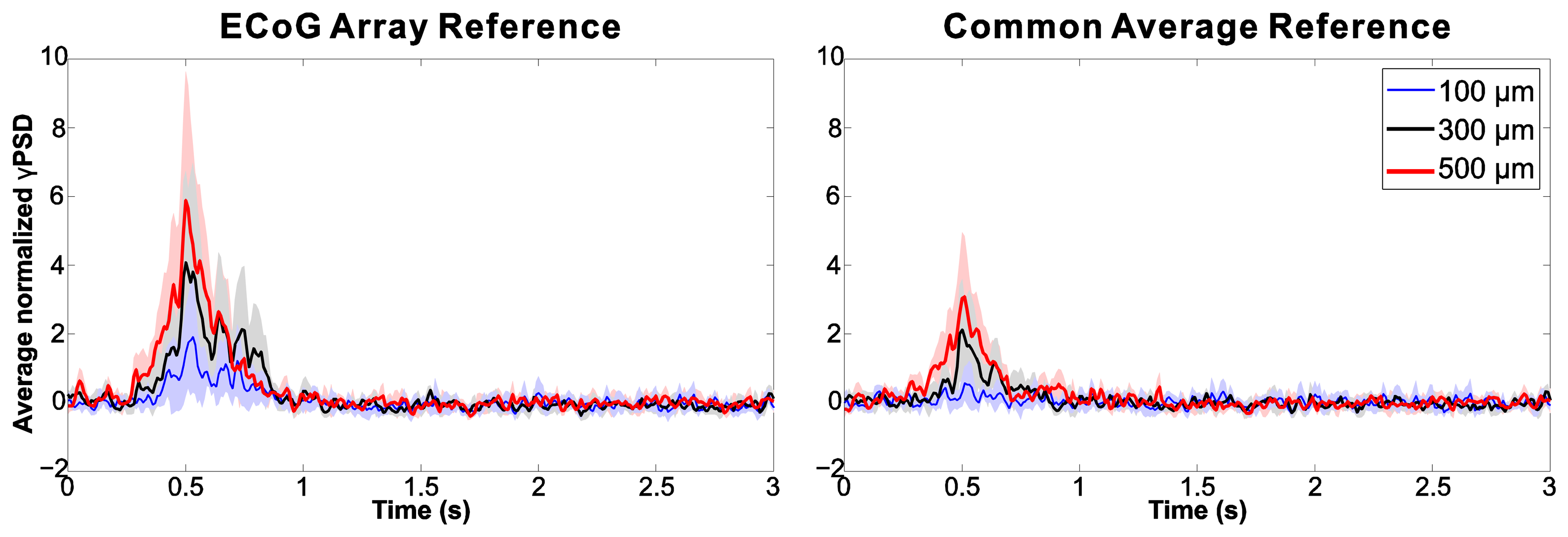
To compare PSD values, 11 triplets of neighbouring electrodes were selected and measured over eight sessions (88 samples in total); the frequency bins between 40 and 150 Hz in the time-frequency matrix were averaged for each electrode to build time courses of average gamma-PSD (γPSD). Figure 17 presents for the three example electrodes the γPSD-time courses obtained with two different referencing methods: the usage of a skull-facing electrode resulted in an almost twofold increase in power value (left image), as compared to common average referencing [64,65] (right image). With respect to γPSD for both referencing techniques the smallest electrodes consistently recorded the smallest spectral power, while the largest electrodes recorded the greatest average γPSD in 71.6% (63/88) of the measurement triplets examined.
To complement the analysis of average PSD values, gamma-band signal-to-noise ratio (SNRγ) measurements were performed and then compared across electrode sizes. SNRγ was measured as the ratio between the mean area beneath the full width at half maximum of the gamma PSD time courses and the standard deviation of the areas, measured over all successful trials in a session displaying the same stimulus. There was no statistically significant difference in SNRγ between neighbouring electrodes of different sizes, χ2(2) = 5.1839, p = 0.0749 (Friedman; n = 88; Medians: [100 μm: 3.43, 300 μm: 2.87, 500 μm: 2.80]).
4. Discussion
In this paper we presented the design of an ECoG electrode array with high-electrode count and density. Electrodes of three different sizes (100, 300 and 500 μm in diameter) and a 2.5 mm2 skull-facing reference electrode were implemented to provide a device for testing their influence on the quality of ECoG signal-acquisition.
The high-electrode count and the array's application on freely-moving animals required a highly miniaturized connector-assembly platform. For this purpose, we developed a microfabrication flow which results in highly flexible 10 μm-thick polyimide (PI) bi-layer, with Ti/Au metallization in it and allows also the monolithic integration of a fully rigid interposer for the assembly of miniature SMD-type Omnetics connectors. The silicon interposer was fabricated via a two-step DRIE etching procedure.
State-of-the-art ECoG arrays are fabricated of polymer/metal/polymer, making use most often of either PI [42,47,49,50,54] or parylene [46,48,51] as flexible materials and of Pt [42] or Au [54,66] as metallization materials. In contrast to the presented device, state-of-the-art ECoG arrays are peeled from their wafer carriers and electrical connections are made by means of zero-insertion-force (ZIF) connectors [46–49], ACF on fan-out PCBs [43,50–53], soldering of through-hole Omnetics connectors [42] or isotropic conductive epoxy [56–58]. Each of the above assembly solutions is advantageous for a certain range of electrode count or array application. Nevertheless, if the focus is set on multi-channel ECoG arrays with connector-assembly area reduced to a minimum, then only soldering of through-hole Omnetics connectors [42] remains as a proposed connector-assembly technique. Compared to the work of [42], our fabrication process requires additional DRIE silicon etching, which increases fabrication time/costs/complexity. Nonetheless, exactly this additional fabrication step turns into a substantial advantage in terms of straightforward connector alignment and assembly and reliable solder-joints, requiring no additional rigid soldering jig to hold the array in place.
Electrical open and short-connection tests showed that fully rigid solder joints were much more reliable than those containing PI under the metallization pads. Moreover, adhesion tests revealed higher adhesion strength of the Si/SiO2-metal interface compared to the Si/SiO2/PI-metal interface, which most likely accounts for the higher reliability of the fully rigid solder joints. Comparing PI/metal adhesion before and after the second polyimide curing indicated a decrease in adhesion at the PI/metal interface, most likely caused by thermal stress exerted during the final curing step.
The array electrodes and its reference have impedance magnitudes that increase as the electrode surface area grows larger, as expected. The impedance magnitude of the reference electrode at 100 Hz is eight times smaller than the impedance of the largest circular electrodes, and the impedance at 100 Hz of the smallest electrodes is ca. 105 times lower than the input impedance of a commercial headstage amplifier [42]. These impedance differences are of considerable importance for recording electrocorticograms with sufficiently high amplitude. Furthermore, the derived parameters of the equivalent electric circuit as suggested by [63] indicated a clear linear relationship between the capacitance and the electrode surface area, while the associated double-layer resistance rose linearly with the inverse of the electrode surface area. Compared to impedance values reported in literature, our measurements are equivalent to impedance values reported by Baek et al. (480 μm diameter) [54] and by Kim et al. (250 μm diameter) [66].
We designed this array layout to investigate the dependence between electrode properties and the characteristics of acquired signals for the rhesus macaque brain. This animal model was chosen because of the anatomical and physiological similarity between macaque and human brains. Furthermore, we could take advantage of the highly specific and well-documented spatial organization of the primary visual cortex, which allows recording stimulus-induced responses from different groups of electrodes according to the position of the visual stimulus shown to the animal. The array covers the cortical region representing visual field regions between one and five degrees of eccentricity, which simplifies the placement of visual stimuli and also facilitates array implantation.
To demonstrate the functionality of our design we implanted the array in a rhesus macaque and successfully recorded electrophysiological signals, including strong and distinct stimulus-induced responses, for several months. The temporal order in which the stimulus-induced responses occurred at the different electrodes was clearly related to the succession of positions traversed by the moving stimuli in the visual field. First recordings of our electrode array indicated that larger electrodes recorded stimulus responses with greater spectral power in the gamma band (40–150 Hz), distinctively stronger than the baseline signal, which can be attributed to the larger recorded population of neurons contributing to the stimulus-induced activity patterns. These in vivo results indicate that the ECoG array construction, design and fabrication were successful.
Furthermore, referencing the recordings to the skull-facing reference electrode provided signals with greater power than those obtained using a common average referencing technique. This difference can be explained by the synchronous activity in the gamma band induced over extended regions of area V1 by the long bar stimulus [67]. This activity is therefore acquired by a substantial subset of the array electrodes and therefore prominently contained in the common average reference which is obtained by averaging over all electrode signals. Subtracting this common average reduces the gamma band response in corresponding electrodes. Further advantages of integrating the reference electrode at the backside of the array are the avoidance of additional effort to place a separate reference during surgery; the saving of space, in particular if multiple arrays are implanted; and the minimization of spurious signals more likely to be picked up by a distant reference electrode facing the brain.
5. Conclusions/Outlook
A flex-rigid ECoG electrode array was proposed, which has high-electrode count and density. The highly flexible nature of the device allows bending from a flat into spherical shape without formation of folds, which matches the cortical surface. The highly planar and rigid connector platform (Si/SiO2), monolithically integrated in the structure of the flexible ECoG array, facilitates the assembly of miniature fine-pitch Omnetics connectors.
Furthermore, circular gold electrodes of three different sizes and high density were implemented in the array's signal-acquisition area. This will enable future investigations on the optimal size and density of ECoG electrodes with respect to different types of brain signals which provide different information content. Such knowledge will be helpful for design and configuration of dedicated brain computer interfaces for different specific purposes.
Epidural electrocorticographic recordings of strong and distinct stimulus-induced electrophysiological field potential signals from a Rhesus macaque's primary visual cortex (V1) demonstrated functioning of the proposed flex-rigid electrode array design. Larger electrodes recorded signals with greater spectral power in the gamma band (40–150 Hz). The use of a skull-facing reference electrode confirmed an expected higher spectral power as compared to the common average reference technique, distinctively stronger than the baseline.
These results support the advantage of engineering a flex-rigid electrode array with a monolithically integrated connector platform for the microfabrication of high-electrode count and density ECoG electrode arrays for neuroprosthetics and brain-computer interfacing applications.
Acknowledgments
This research was funded by Bundesministerium für Bildung und Forschung (BMBF), Grant 01EZ 0867 (Innovationswettbewerb Medizintechnik) and by the German Excellence Initiative via the Creative Unit “I-See”. The authors highly appreciate the discussions with Ingrid Michels, Ibrahim Erzoes, and Praveen Pratti on connector assembly. The authors thank Eva-Maria Meyer for making the SEM images, and Katja Taylor, Katrin Thoβ and Ramazani Hakizimana for assistance with animal training and daily care.
Author Contributions
E.T. designed the flex-rigid device. E.T., L.K. and V.B. performed the device microfabrication. E.T. and V.G.-G. conducted the EIS tests. V.G.-G. designed the signal-acquisition area of the ECoG array. V.G.-G., S.M. and A.K.K. were involved in the array implantation. V.G.-G. performed in vivo recoding & data analysis. S.M. supported in vivo data recording & analysis. A.K.K. conducted planning of in vivo experiments, supervision of in vivo recording & data analysis. W.L. conducted planning of technology and evaluation of EIS experiments. All authors contributed to writing of this paper.
Conflicts of Interest
The authors declare no conflict of interest.
References
- Rotermund, D.; Ernst, U.A. Toward high performance, weakly invasive Brain Computer Interfaces using selective visual attention. J. Neurosci. 2013, 33, 6001–6011. [Google Scholar]
- Freeman, W.J.; Rogers, L.J. Spatial spectral analysis of human electrocorticograms including the alpha and gamma bands. J. Neurosci. Methods 2000, 95, 111–121. [Google Scholar]
- Slutzky, M.W.; Jordan, L.R. Optimal spacing of surface electrode arrays for brain-machine interface applications. J. Neur. Eng. 2010, 7. [Google Scholar] [CrossRef]
- Freeman, W.J.; Holmes, M.D. Spatial spectra of scalp EEG and EMG from awake humans. Clin. Neurophysiol. 2003, 114, 1053–1068. [Google Scholar]
- Ball, T.; Kern, M. Signal quality of simultaneously recorded invasive and non-invasive EEG. Neuroimage 2009, 46, 708–716. [Google Scholar]
- Staba, R.J.; Wilson, C.L. Quantitative analysis of high-frequency oscillations (80–500 Hz) recorded in human epileptic hippocampus and entorhinal cortex. J. Neurophysiol. 2002, 88, 1743–1752. [Google Scholar]
- Menon, V.; Freeman, W.J. Spatio-temporal correlations in human gamma band electrocorticograms. Electroencephalogr. Clin. Neurophysiol. 1996, 98, 89–102. [Google Scholar]
- Crone, N.E.; Miglioretti, D.L. Functional mapping of human sensorimotor cortex with electrocorticographic spectral analysis. II. Event-related synchronization in the gamma band. Brain 1998, 121, 2301–2315. [Google Scholar]
- Crone, N.E.; Hao, L. Electrocorticographic gamma activity during word production in spoken and sign language. Neurology 2001, 57, 2045–2053. [Google Scholar]
- Taylor, K.; Mandon, S. Coherent oscillatory activity in monkey area v4 predicts successful allocation of attention. Cerebr. Cortex 2005, 15, 1424–1437. [Google Scholar]
- Schalk, G.; Kubanek, J. Decoding two-dimensional movement trajectories using electrocorticographic signals in humans. J. Neur. Eng. 2007, 4. [Google Scholar] [CrossRef]
- Acharya, S.; Fifer, M.S. Electrocorticographic amplitude predicts finger positions during slow grasping motions of the hand. J. Neur. Eng. 2010, 7. [Google Scholar] [CrossRef]
- Chao, Z.C.; Nagasaka, Y. Long-term asynchronous decoding of arm motion using electrocorticographic signals in monkeys. Fronti. Neuroeng. 2010, 3. [Google Scholar] [CrossRef]
- Gunduz, A.; Brunner, P. Neural correlates of visual–spatial attention in electrocorticographic signals in humans. Front. Hum. Neurosci. 2011, 5. [Google Scholar] [CrossRef]
- Chestek, C.A.; Gilja, V. Hand posture classification using electrocorticography signals in the gamma band over human sensorimotor brain areas. J. Neur. Eng. 2013, 10. [Google Scholar] [CrossRef]
- He, B.J.; Snyder, A.Z. Electrophysiological correlates of the brain's intrinsic large-scale functional architecture. Proc. Natl. Acad. Sci. USA 2008, 105, 16039–16044. [Google Scholar]
- Nir, Y.; Mukamel, R. Interhemispheric correlations of slow spontaneous neuronal fluctuations revealed in human sensory cortex. Nat. Neurosci. 2008, 11, 1100–1108. [Google Scholar]
- Conner, C.R.; Ellmore, T.M. Variability of the relationship between electrophysiology and BOLD-fMRI across cortical regions in humans. J. Neurosci. 2011, 31, 12855–12865. [Google Scholar]
- Tallon-Baudry, C.; Mandon, S. Oscillatory synchrony in the monkey temporal lobe correlates with performance in a visual short-term memory task. Cerebr. Cortex 2004, 14, 713–720. [Google Scholar]
- Bosman, C.A.; Schoffelen, J.M. Attentional stimulus selection through selective synchronization between monkey visual areas. Neuron 2012, 75, 875–888. [Google Scholar]
- Grothe, I.; Neitzel, S.D. Switching neuronal inputs by differential modulations of gamma-band phase-coherence. J. Neurosci. 2012, 32, 16172–16180. [Google Scholar]
- Loeb, G.E.; Walker, A.E. Histological reaction to various conductive and dielectric films chronically implanted in the subdural space. J. Biomed. Mater. Res. 1977, 11, 195–210. [Google Scholar]
- Bullara, L.A.; Agnew, W.F. Evaluation of electrode array material for neural prostheses. Neurosurgery 1979, 5, 681–686. [Google Scholar]
- Yuen, T.G.; Agnew, W.F. Tissue response to potential neuroprosthetic materials implanted subdurally. Biomaterials 1987, 8, 138–141. [Google Scholar]
- Williams, J.C.; Hippensteel, J.A. Complex impedance spectroscopy for monitoring tissue responses to inserted neural implants. J. Neur. Eng. 2007, 4, 410–423. [Google Scholar]
- Thelin, J.; Jörntell, H. Implant size and fixation mode strongly influence tissue reactions in the CNS. PLoS One 2011, 6. [Google Scholar] [CrossRef]
- Leuthardt, E.C.; Schalk, G. A brain-computer interface using electrocorticographic signals in humans. J. Neur. Eng. 2004, 1, 63–71. [Google Scholar]
- Leuthardt, E.C.; Miller, K.J.; Schalk, G. Electrocorticography-based brain computer interface—The Seattle experience. IEEE Trans. Neur. Syst. Rehabil. Eng. 2006, 14, 194–198. [Google Scholar]
- Wilson, J.A.; Felton, E.A.; Garell, P.C. ECoG factors underlying multimodal control of a brain-computer interface. IEEE Trans. Neur. Syst. Rehabil. Eng. 2006, 14, 246–250. [Google Scholar]
- Felton, E.A.; Wilson, J.A. Electrocorticographically controlled brain-computer interfaces using motor and sensory imagery in patients with temporary subdural electrode implants: Report of four cases. J. Neurosurg. 2007, 106, 495–500. [Google Scholar]
- Hinterberger, T.; Widman, G. Voluntary brain regulation and communication with electrocorticogram signals. Epilepsy Behav. 2008, 13, 300–306. [Google Scholar]
- Schalk, G.; Miller, K.J. Two-dimensional movement control using electrocorticographic signals in humans. J. Neur. Eng. 2008, 5. [Google Scholar] [CrossRef]
- Rouse, A.G.; Moran, D.W. Neural adaptation of epidural electrocorticographic (EECoG) signals during closed-loop brain computer interface (BCI) tasks. Proceedings of the Engineering in Medicine and Biology Society (IEEE EMBC), Minneapolis, MN, USA, 3–6 September 2009; pp. 5514–5517.
- Rotermund, D.; Taylor, K. Attention improves object representation in visual cortical field potentials. J. Neurosci. 2009, 29, 10120–10130. [Google Scholar]
- Yanagisawa, T.; Hirata, M. Electrocorticographic control of a prosthetic arm in paralyzed patients. Ann. Neurol. 2012, 71, 353–361. [Google Scholar]
- Rouse, A.G.; Williams, J.J. Cortical adaptation to a chronic micro-electrocorticographic brain computer interface. J. Neurosci. 2013, 33, 1326–1330. [Google Scholar]
- Wang, W.; Collinger, J.L. An electrocorticographic brain interface in an individual with tetraplegia. PLoS One 2013, 8. [Google Scholar] [CrossRef]
- Schalk, G.; Leuthardt, E.C. Brain-computer interfaces using electrocorticographic signals. IEEE Rev. Biomed. Eng. 2011, 4, 140–154. [Google Scholar]
- Blakely, T.; Miller, K.J. Robust, long-term control of an electrocorticographic brain-computer interface with fixed parameters. Neurosurg. Focus 2009, 27. [Google Scholar] [CrossRef]
- Kellis, S.S.; House, P.A. Human neocortical electrical activity recorded on nonpenetrating microwire arrays: Applicability for neuroprostheses. Neurosurg. Focus 2009, 27. [Google Scholar] [CrossRef]
- Kim, D.H.; Viventi, J. Dissolvable films of silk fibroin for ultrathin conformal bio-integrated electronics. Nat. Mater. 2010, 9, 511–517. [Google Scholar]
- Rubehn, B.; Bosman, C. A MEMS-based flexible multichannel ECoG-electrode array. J. Neur. Eng. 2009, 6. [Google Scholar] [CrossRef]
- Viventi, J.; Kim, D.H. Flexible, foldable, actively multiplexed, high-density electrode array for mapping brain activity in vivo. Nat. Neurosci. 2011, 14, 1599–1605. [Google Scholar]
- Wang, W.; Degenhart, A.D. Human motor cortical activity recorded with Micro-ECoG electrodes, during individual finger movements. Proceedings of the Engineering in Medicine and Biology Society (IEEE EMBC), Minneapolis, MN, USA, 3–6 September 2009; pp. 586–589.
- Nelson, M.J.; Pouget, P. Physical model of coherent potentials measured with different electrode recording site sizes. J. Neurophysiol. 2012, 107, 1291–1300. [Google Scholar]
- Gutierrez, C.A.; Lee, C. Epoxy-less packaging methods for electrical contact to parylene-based flat flexible cables. Proceedings of the 16th International IEEE Solid-State Sensors, Actuators and Microsystems Conference (TRANSDUCERS), Beijing, China, 5–9 June 2011; pp. 2299–2302.
- Lee, K.K.; He, J. Polyimide-based intracortical neural implant with improved structural stiffness. J. Micromech. Microeng. 2004, 14. [Google Scholar] [CrossRef]
- Metallo, C.; White, R.D. Flexible parylene-based microelectrode arrays for high resolution EMG recordings in freely moving small animals. J. Neurosci. Methods 2011, 195, 176–184. [Google Scholar]
- Myllymaa, S.; Myllymaa, K. Fabrication and testing of polyimide-based microelectrode arrays for cortical mapping of evoked potentials. Biosens. Bioelectron. 2009, 24, 3067–3072. [Google Scholar]
- Baek, D.H.; Park, J.S. Interconnection of multichannel polyimide electrodes using anisotropic conductive films (ACFs) for biomedical applications. IEEE Trans. Biomed. Eng. 2011, 58, 1466–1473. [Google Scholar]
- Ledochowitsch, P.; Félus, R.J. Fabrication and testing of a large area, high density, parylene MEMS μECoG array. Proceedings of the IEEE 24th International Conference on Micro Electro Mechanical Systems (MEMS), Cancun, Mexico, 23–27 January 2011; pp. 1031–1034.
- Ledochowitsch, P.; Tiefenauer, R.F. Nanoflex for neural nanoprobes. Proceedings of the Transducers & Eurosensors XXVII Solid-State Sensors, Actuators and Microsystems (TRANSDUCERS & EUROSENSORS XXVII), Barcelona, Spain, 16–20 June 2013; pp. 1278–1281.
- Wu, F.; Tien, L. A multi-shank silk-backed parylene neural probe for reliable chronic recording. Proceedings of 2013 Transducers & Eurosensors XXVII Solid-State Sensors, Actuators and Microsystems (TRANSDUCERS & EUROSENSORS XXVII), Barcelona, Spain, 16–20 June 2013; pp. 888–891.
- Baek, D.H.; Han, C.H. Soldering-based easy packaging of thin polyimide multichannel electrodes for neuro-signal recording. J. Micromech. Microeng. 2012, 22. [Google Scholar] [CrossRef]
- Fiedler, E.; Ordonez, J. Modular assembly of flexible thin-film electrode arrays enabled by a laser-structured ceramic adapter. Proceedings of the 6th International IEEE/EMBS Conference on Neural Engineering (NER), San Diego, CA, USA, 6–8 November 2013; pp. 657–660.
- Rousche, P.J.; Pellinen, D.S. Flexible polyimide-based intracortical electrode arrays with bioactive capability. IEEE Trans. Biomed. Eng. 2001, 48, 361–371. [Google Scholar]
- Mercanzini, A.; Cheung, K. Demonstration of cortical recording using novel flexible polymer neural probes. Sens. Actuators A Phys. 2008, 143, 90–96. [Google Scholar]
- Sankar, V.; Sanchez, J.C. A highly compliant serpentine shaped polyimide interconnect for front-end strain relief in chronic neural implants. Front. Neurol. 2013, 4. [Google Scholar] [CrossRef]
- Mimoun, B.; Henneken, V. Flex-to-Rigid (F2R): A novel ultra-flexible technology for smart invasive medical instruments. Proceedings of the MRS Symposium on Stretchable Electronics and Conformal Biointerfaces, San Francisco, CA, USA, 8–9 April 2010.
- Tolstosheeva, E.; Gordillo-González, V. A novel flex-rigid and soft-release ECoG array. Proceedings of the Engineering in Medicine and Biology Society (IEEE EMBC), Boston, MA, USA, 30 August– 3 September 2011; pp. 2973–2976.
- Tolstosheeva, E.; Hoeffmann, J. Towards a wireless and fully-implantable ECoG system. Proceedings of the Transducers & Eurosensors XXVII on Solid-State Sensors, Actuators and Microsystems (TRANSDUCERS & EUROSENSORS XXVII), Barcelona, Spain, 16–20 June 2013; pp. 384–387.
- Rabilloud, G. High-performance polymers: Chemistry and applications. Ed. OPHRYS 2000, 2, 129–130. [Google Scholar]
- Geddes, L.A. Historical evolution of circuit models for the electrode-electrolyte interface. Ann. Biomed. Eng. 1997, 25, 1–14. [Google Scholar]
- Offner, F.F. The EEG as potential mapping: The value of the average monopolar reference. Electroencephalogr. Clin. Neurophysiol. 1950, 2, 213–214. [Google Scholar]
- Ludwig, K.A. Using a common average reference to improve cortical neuron recordings from microelectrode arrays. J. Neurophysiol. 2009, 101, 1679–1689. [Google Scholar]
- Kim, J. A cortical recording platform utilizing μECoG electrode arrays. Proceedings of the Engineering in Medicine and Biology Society (IEEE EMBC), Lyon, France, 23–26 August 2007; pp. 5353–5357.
- Maldonado, P.E.; Friedman-Hill, S.R.; Gray, C.M. Dynamics of striate cortical activity in the alert macaque: II. Fast time scale synchronization. Cereb. Cortex 2000, 10, 1117–1131. [Google Scholar]


| Electrode Diameter | Electrode Area [mm2] | Rs [kΩ] | Rp [MΩ] | C [nF] |
|---|---|---|---|---|
| 100 μm | 0.031 | 2.6 ± 0.1 | 83.5 ± 31.7 | 1.3 ± 0.1 |
| 300 μm | 0.283 | 1.8 ± 0.02 | 4.8 ± 0.4 | 10.6 ± 0.4 |
| 500 μm | 0.783 | 1.5 ± 0.02 | 1.3 ± 0.1 | 36.0 ± 3.1 |
© 2015 by the authors; licensee MDPI, Basel, Switzerland. This article is an open access article distributed under the terms and conditions of the Creative Commons Attribution license ( http://creativecommons.org/licenses/by/4.0/).
Share and Cite
Tolstosheeva, E.; Gordillo-González, V.; Biefeld, V.; Kempen, L.; Mandon, S.; Kreiter, A.K.; Lang, W. A Multi-Channel, Flex-Rigid ECoG Microelectrode Array for Visual Cortical Interfacing. Sensors 2015, 15, 832-854. https://doi.org/10.3390/s150100832
Tolstosheeva E, Gordillo-González V, Biefeld V, Kempen L, Mandon S, Kreiter AK, Lang W. A Multi-Channel, Flex-Rigid ECoG Microelectrode Array for Visual Cortical Interfacing. Sensors. 2015; 15(1):832-854. https://doi.org/10.3390/s150100832
Chicago/Turabian StyleTolstosheeva, Elena, Víctor Gordillo-González, Volker Biefeld, Ludger Kempen, Sunita Mandon, Andreas K. Kreiter, and Walter Lang. 2015. "A Multi-Channel, Flex-Rigid ECoG Microelectrode Array for Visual Cortical Interfacing" Sensors 15, no. 1: 832-854. https://doi.org/10.3390/s150100832