Thermoresistive Strain Sensor and Positioning Method for Roll-to-Roll Processes

Abstract
: This study uses the Joule heating effect-generated temperature difference to monitor in real-time and localize both compressive and tensile strains for the polymer substrates used in the roll-to-roll process. A serpentine gold (Au) line was patterned on a polyethylenenaphthalate (PEN) substrate to form the strain sensor based on thermoresistive behavior. This strain sensor was then subjected to either current or voltage to induce the Joule heating effect on the Au resistor. An infrared (IR) detector was used to monitor the strain-induced temperature difference on the Au and PEN surfaces and the minimal detectable bending radius was 0.9 mm with a gauge factor (GF) of 1.46. The proposed design eliminates the judgment ambiguity from conventional resistive strain sensors where resistance is the only physical quantity monitored. This study precisely and successfully indicated the local strain quantitatively and qualitatively with complete simulations and measurements.1. Introduction
Strain sensors are widely used to evaluate material and structural failures or weak points. Because strains generated in the micrometer range are difficult to visualize in real-time using the bare eyes, they must be detected based on physical quantities read out by humans or automatic systems. Light-based optical strain detection solutions usually take advantage of unique optical effects, such as the Fabry-Pérot interference [1,2], the Moiré effect [3,4], Bragg diffraction [5,6], or pattern recognition [7], to visualize strain with visible colors or non-visible signals. In the same time, sound waves are also used to monitor the density of materials, which in turn reflect strains embedded inside. The surface acoustic wave (SAW) system [8] is one of the strain sensors that take advantage of sound waves. Other novel strain sensors based on X-rays [9] and radio waves [10] were not considered and compared here because of their complicated setup and higher power consumption.
In addition to optical and acoustical strain sensors, other physical quantities like resistance [11,12], capacitance [13,14], inductance [15], and magnetic field [16] are also used to measure strains. Among these options resistive strain sensors are widely used because of their simple detection mechanism. Resistance varies in proportion to the resistor length change, and the material strain exhibits a relationship with the resistance. Corrections are occasionally necessary because the thickness and width of a resistor also change with its change of length. Table 1 lists conventional resistive strain sensors with their characteristics, where the sensitivity represents the smallest detectable strain in the corresponding system, and the negative and positive signs represent compression and tension in the strain detection range, respectively. The definition and calculation of the gauge factor will be described later.
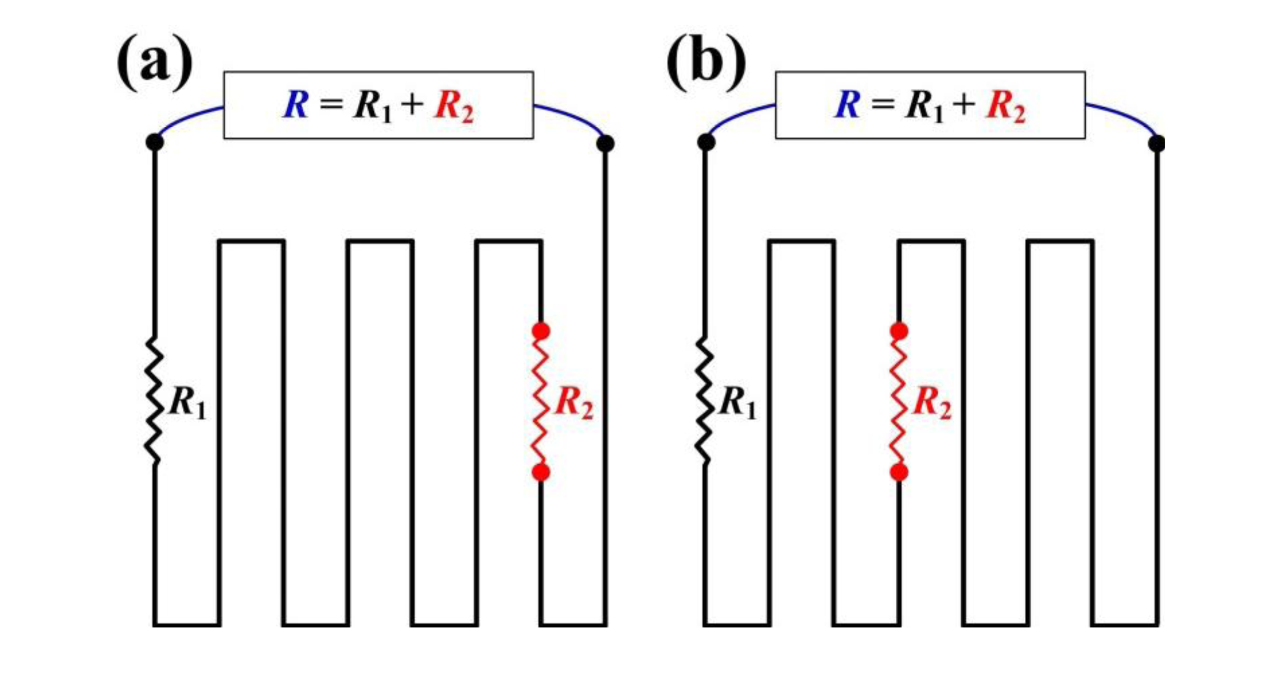
Nevertheless, these resistive strain sensors use only one physical quantity–resistance–and lack application variety and location accuracy. The output signals from a resistive strain sensor only reflect overall performance, and overlook local details. For example, when a target object has one small-value-tension connected in series to another large-value-compression, the monitored resistance returns only a superimposed result of a small-value-compression. Similar ambiguity also appears for resistors for strain sensor applications connected in parallel. This overlooked result is misleading and leads to incorrect judgments (Figure 1).
From the roll-to-roll (R2R) mass production viewpoint, a methodology that detects substrate strains in real-time is necessary, otherwise the tens to thousands of meter-long substrates shift during winding and unwinding. This represents a critical manufacturing issue for flexible electronic devices, where micrometer or nanometer registration (alignment) shifts can result in device malfunction or failure. This pattern shift will be further worsened if a multiple layer stack is used for the device. Previous work proposed a detection methodology for the starring and telescoping effect in the R2R system [21]. However, it requires external strain sensors with wound rolls before the uneven stress distribution can be returned to the controller and then adjusted by mechanical parts. Although it solved off-line the winding/unwinding shifts, it neither handles micrometer strains nor corrects the shifts in real-time. Furthermore, the external strain sensor arrangement is a manual task, which cannot be performed automatically. To solve these issues, this study proposes an advanced resistive strain sensor that introduces a second physical quantity of heat to localize the strain quantitatively, qualitatively, and automatically.
2. Design
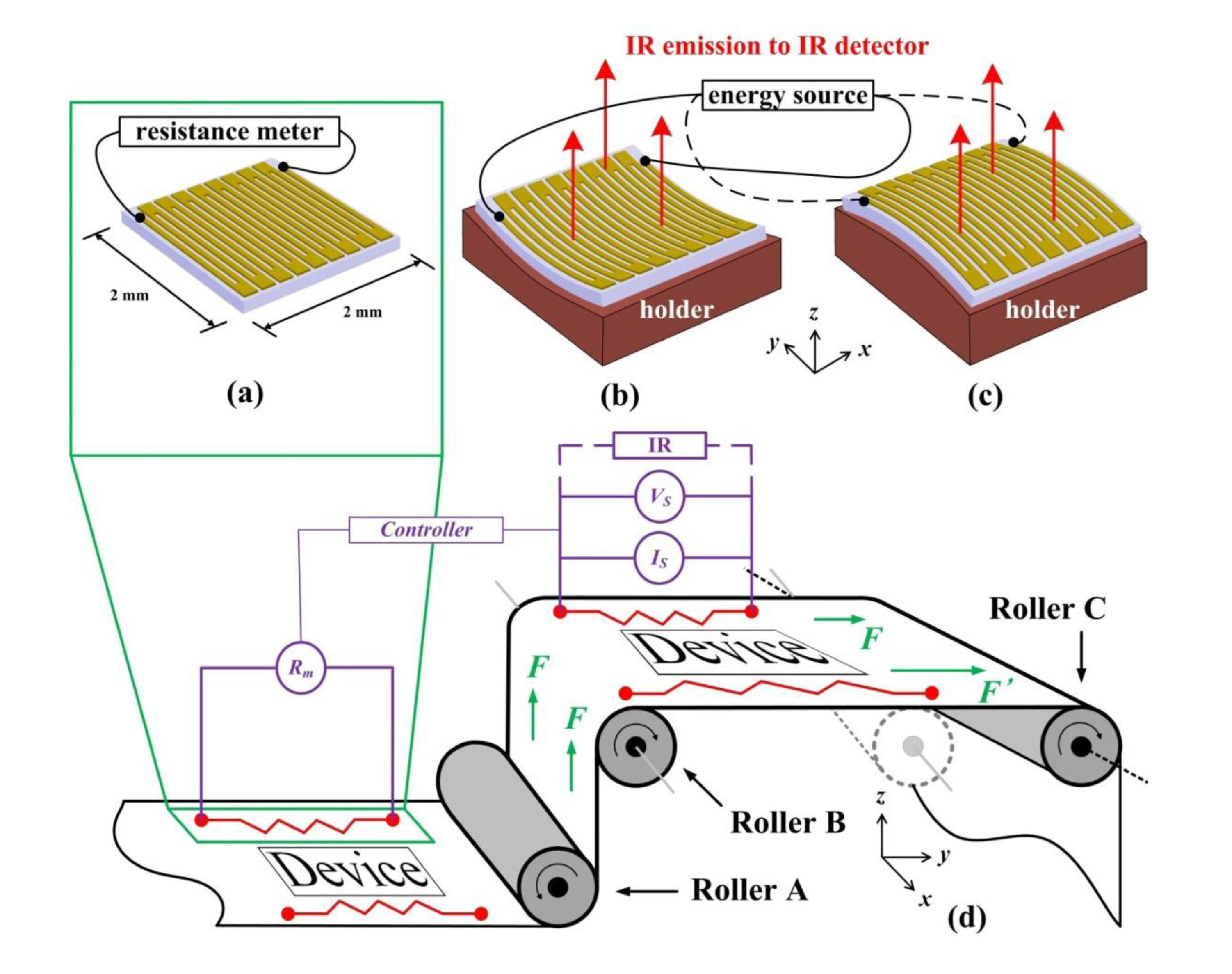
Figure 2 shows the proposed device and the detection system setup. A serpentine metal resistor was patterned by lithography on the polymer substrate with large routing pads at both ends. A 125 μm thick polyethylenenaphthalate (PEN; Teijin DuPont, Q65F, Wilmington, DE, USA) was chosen as the substrate to reflect the reality of a roll-to-roll manufacturing system for flexible electronic device applications, which generally faces mechanical accuracy (strain) issues (Figure 2d). Gold (Au) of thickness of 10 nm was chosen as the resistor because of its sensitive electrical properties and good thermal conductivity during application and measurement. The Au resistor was directly patterned on the PEN by photolithography without adhesion concerns [22] in this study. Other polymer substrates and metal resistors can also be used similarly to this proposed scenario.
3. Principle
During operation, a current (I) or voltage (V) is applied to the Au resistor with resistance (R), which generates thermal energy (heat, P) because of the Joule heating effect. The thermal energy is positively (P = I2R) and negatively (P = V2/R) related to the resistance under a fixed current or voltage, respectively. When the PEN substrate and the Au resistor above it change their dimensions, the resistance changes accordingly. With the aforementioned Joule heating effect, users can obtain deformation and strain information by understanding the infrared (IR) emissions from the Au resistors located on both sides of the substrate.
The sensitive electrical behavior of 10-nm-thick Au enhanced the temperature change because its resistance highly reflects the dimensional change. The operation of this proposed methodology uses the resistance change (ΔR) instead of absolute resistance value (R), thus slight initial resistance variations caused by the patterning process before Roller A do not contribute to the temperature change (ΔT). Use of a well-developed and commercially available resistance meter (Rm) with controllers to adjust voltage source (Vs) or current source (Is) in Figure 2d further eliminate the initial resistance variation concern, which is outside the scope of this study.
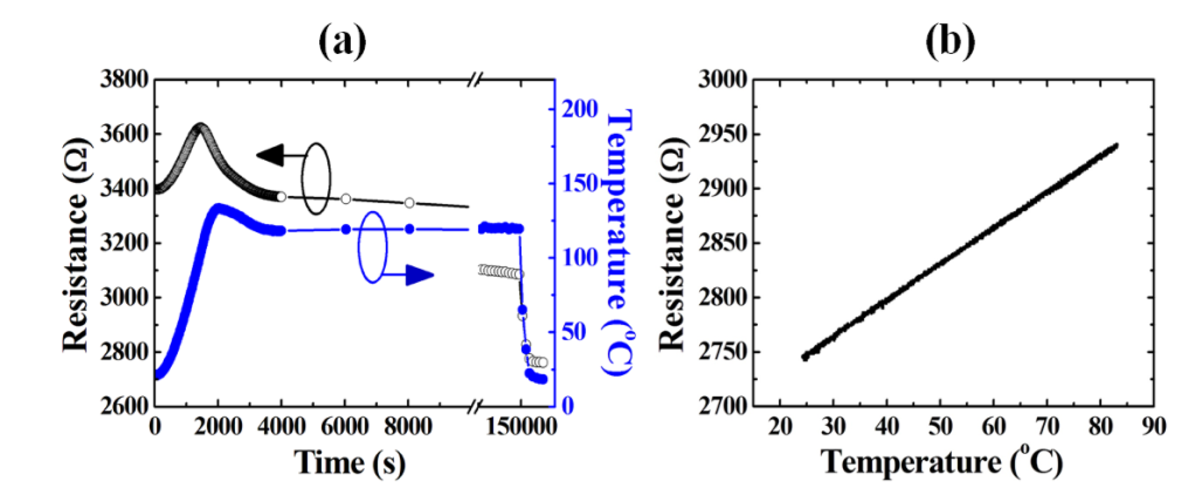
On the other hand, the Joule heating effect also gradually reduces the resistance of Au because of metal sintering [23]. In order to decouple the influence of the metal sintering from the strain measurement, a preliminary thermal treatment (120 °C, 36 h) was applied to the Au/PEN structure to greatly reduce the resistance of Au and to generate a stable, metal sintering-ineffective Au (Figure 3a). The linear thermal conductivity of the Au resistor after preliminary thermal sintering assured a linear response between the resistance change and its Joule heating temperature change (ΔT, Figure 3b).
For flexible electronic device structures, extra protections (barriers) are required for reliability enhancement. This study proposes a strain detection methodology based on resistance and infrared emission changes, and does not apply extra protection layer on top of the Au resistor.
4. Simulation
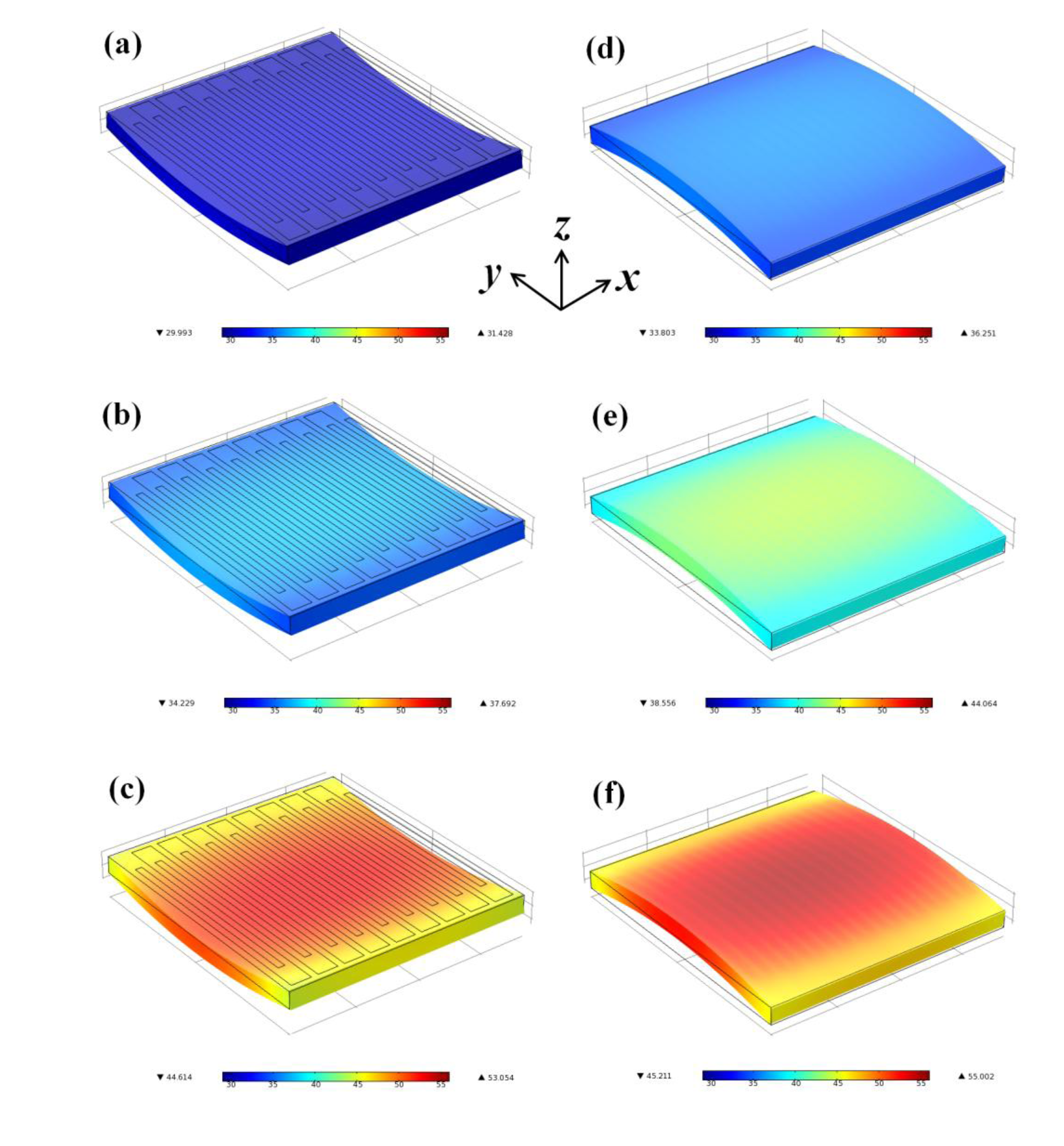
This study used a mechanical-electrical-thermal coupling model for a simulation using the commercial software COMSOL (version 4.0, COMSOL Inc., Burlington, MA, USA). A full-size model was prepared for the simulation by repeating a single straight Au resistor with 50 μm width, 50 μm space, and 1,500 μm length 18 times with routing pads at two ends (Figure 2a). The routing pads had a larger dimension (150 μm wide and 200 μm long) in the y-direction to ensure that the pattern change perpendicular to the loading direction (the x-direction) has a negligible influence on the resistance. Because the thermal conductivity of the PEN is far smaller than that of the Au [24,25], this simulation assumed that the heat transfers mainly through the Au/air interface (the upward heat). Furthermore, when the small portion of heat transfers from the Au to the PEN substrate (the downward heat), it transfers to the surrounding PEN substrate in the ±x-, ±y-, and –z-directions sequentially.
Figure 4a–c shows the simulated temperature results for the compression case with various bending radii under fixed current (I) application. The heat generated with P = I2R distributes across the strain sensor but only accumulates at the center because the heat at the strain sensor edges transfers to the surrounding PEN substrate as mentioned before. Consequently, the temperature distribution on the surface of the strain sensor has its highest value at the center and gradually decreases outwards.
Figure 4d–f shows the simulated temperature results for the tension case with various bending radii under fixed voltage (V) supply with P = V2/R. Like the temperature distribution of the compression case, the temperature has its highest value at the center and its lowest value at the edge of the strain sensor.
5. Results and Discussion
Figure 2b,c illustrates the measurement setup. An IR scope (InfraScope II, QFI Corporation, Vista, CA, USA) was used to monitor the IR emissions from the Au resistor, producing a temperature distribution map during measurement. The environmental temperature was kept at 20 °C for all cases and the resulting temperature map not only reflects the overall average temperature, but also indicates the temperatures at individual points. Owing to the current holder limitations, bending radii (r) between 25 and 200 mm were examined. The strains calculated from the sensor dimensions and their bending radii [26] were between 0.065% (r = 25 mm) and 0.526% (r = 200 mm) for both the compression and the tension cases, which satisfy the reasonable mechanical accuracy requirement of the rollers in the R2R system with substrate side-to-side width (the x-direction) of 100–300 mm (Figure 2d).
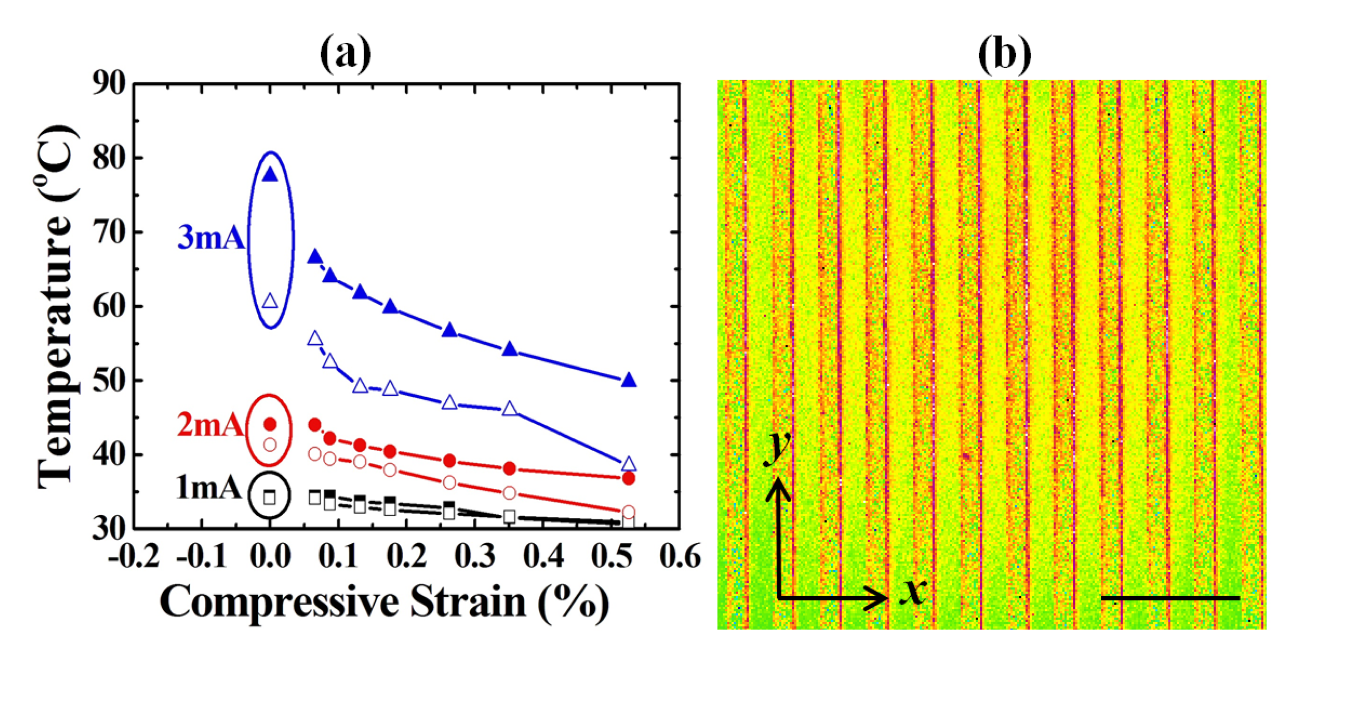
5.1. Compression
Figure 5a shows the relationship between the strains and the measured temperatures of the compression cases. Figure 5b shows the temperature map of an r = 150 mm compression case. The proposed methodology distinguished the bending radii from 25 to 200 mm with the reference of a flat surface point (r = infinite, strain ε = 0%). The difference between the simulated and measured data results from the variations of simulation parameters (the convection heat transfer coefficient, h, and the thermal conductivity, k) [27], which depend on the metal sintering-related grain conditions in thin film instead of in bulk material. This difference was negligible under small currents and was enhanced under large current supply. However, the measured data successfully followed the simulation trend, which represented its eligibility for strain prediction from the relative temperature (resistance) changes, instead of from the absolute temperature (resistance) values. The proposed methodology only compared the resistive change (ΔR) and both the simulations and the experiment results showed the same ΔR and thus, the same ΔT.
5.2. Tension
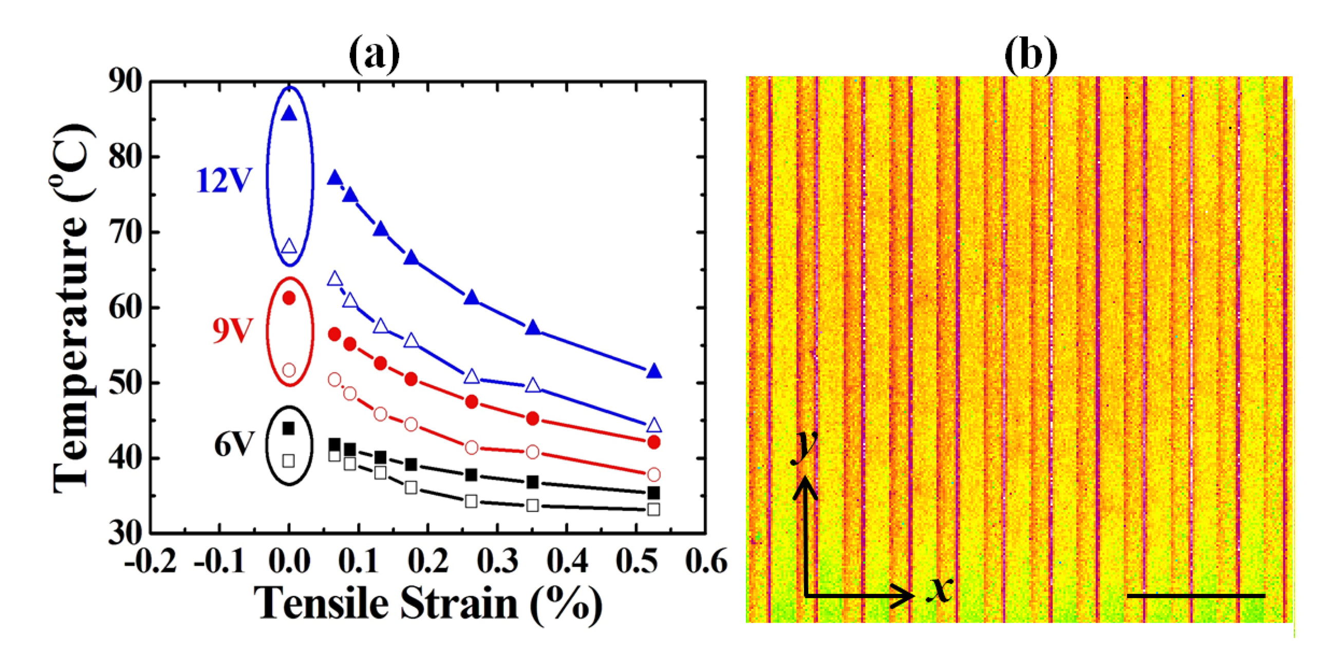
Figure 6a shows the relationship between the strains and the measured temperatures of the tension cases. The trend and sensitivity of the tension case are similar to those of the compression case. Figure 6b shows the temperature map of an r = 150 mm tension case.
5.3. Roll-to-Roll Off-Axis Detection
One of the applications of this proposed methodology is the roll-to-roll manufacturing and is illustrated in Figure 2d. A roll-to-roll system usually contains tens of rollers and the flexible polymer substrate is slightly stretched by these rollers to assure flat substrate surfaces during the process. However, the mechanically controlled tension is usually not precisely balanced from roller to roller.
As a result, the polymer substrate is very possibly stretched more on one side than the other side of a roller. The devices made on the polymer substrate are thus deformed by this issue and their performances suffer from these unpredictable stress-induced strains. For a 500 mm-long (in the y-direction) substrate between rollers B and C in Figure 2d, a 1% strain in one side along the mechanical direction (the y-direction) represents a 5 mm (5000 μm) extension, which is already an unacceptable value in practice for flexible electronic devices of micrometer or nanometer scales. By intentionally differentiating external forces F and F′ in Figure 2d with 1% strain, the results show that the unstressed side (F) did not show a distinguishable temperature difference (69.1 °C at 12 V, compared with the control point of 67.9 °C in Figure 6a) while the stressed side with 1% strain side (F′) showed an absolute value of 39.8 °C at 12 V. The 39.8 °C represents a 0.97% strain, which falls on the extrapolated part of the trend line in Figure 6a and proves the correctness of this methodology.
5.4. Strain Localization
Another major benefit of the proposed methodology is its ability to localize the strain distributed within the sensing area. Figure 1 shows that the superimposed resistances and their changes of the conventional resistive strain sensors are the same. As a result, the resistances in Figure 1 are both R, which overlooks the strain distribution and leads to misjudgment. This issue can only be fixed by an array consisting of smaller strain sensors, but this solution also increases the complexity of the circuit routing, pattern design, sensing methodology, and analysis algorithm. Thus, keeping the same strain sensor configuration but introducing a second physical quantity of heat provides a superior detection resolution as proposed by this study.
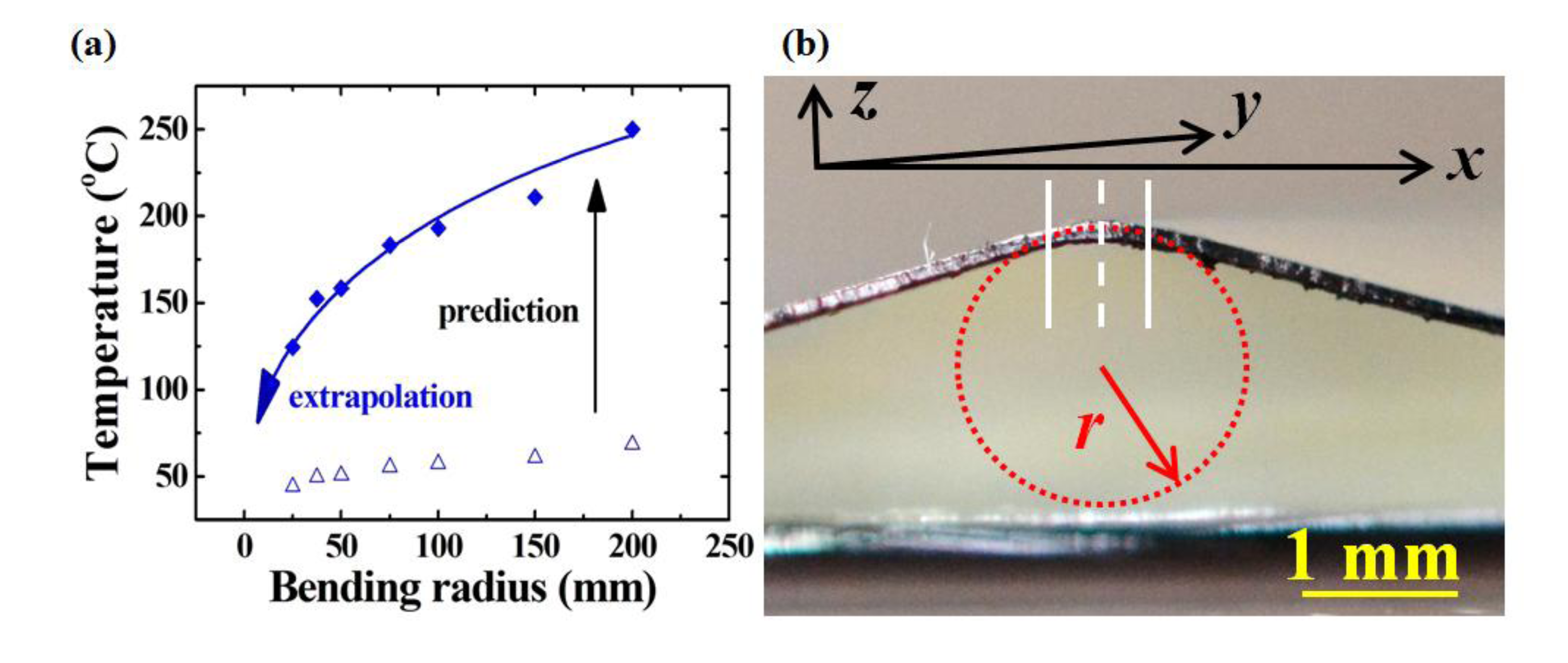
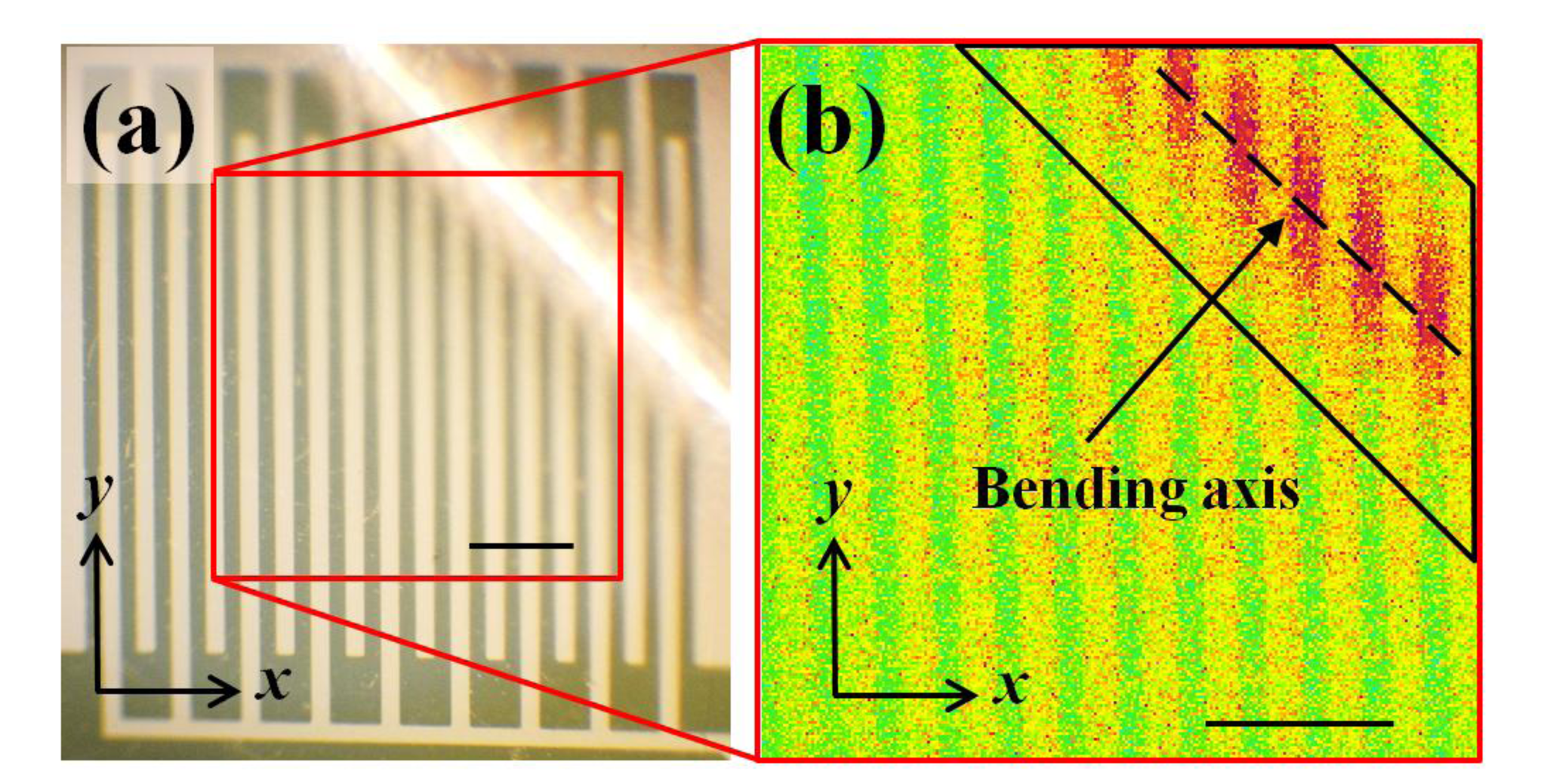
As Figure 7a shows, the strain sensor was intentionally folded at one corner. Figure 7b shows the measurement result, which clearly indicates that the heat accumulated at the surrounding areas of the folding mark. Because the resistance changed mainly at the target (trapezoid) area, the temperature change reflected the location of the strain instead of an overlooked overall behavior.
The dashed line in Figure 7b represents the bending axis and the trapezoid extended 250 μm from the bending axis in each direction. According to the heat transfer model [28], this trapezoid covers 83% of the total heat distribution. A smaller trapezoid area contains higher ratio of the high-temperature image pixels but a smaller trapezoid area cannot cover the whole bending area to reflect the reality. In contrary, a larger trapezoid area covers more sample surfaces but a larger trapezoid area also includes less high-temperature image pixels and results in less accuracy. For this study, a 83% coverage was used to evaluate the sensitivity. The trend of the extrapolation line in Figure 8a predicts that the bending radius of the folding mark in Figure 7a was 0.9 mm with the average temperature of 42.6 °C in the trapezoid area in Figure 7b.
The prediction was calculated from the resistance in series with partial contributions (Figure 1). The folding mark was also optically observed (Figure 8b) for comparison, and the bending radius (0.87 mm) agreed with the prediction. This result validated the proposed methodology with a less than 3.3% difference and the gauge factor (GF) of this proposed strain sensor, which is defined as:
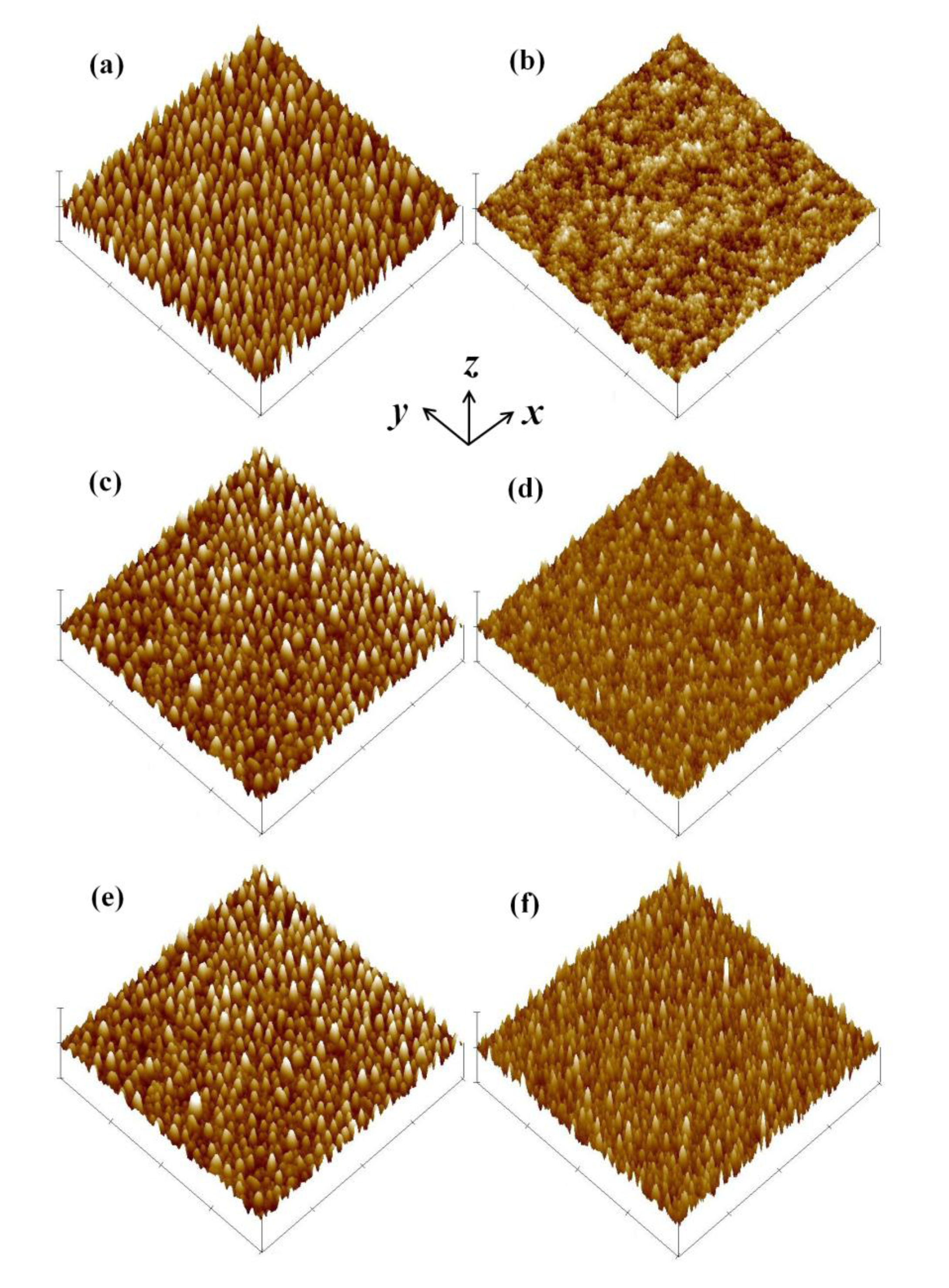
5.5. Surface Morphology and Reliability
The Poisson ratio difference between PEN and Au [29,30] generates different dimensional reductions or extensions under various strains. Metallic Au has better ductility than polymeric PEN and thus extreme volumetric changes of Au on PEN with severe bending potentially produce different surface morphologies. Because the surface morphology of metal reflects its resistance [31,32], it is important to understand the surface roughness and to decouple the dimensional resistance change from morphological influences.
Figure 9 shows the surface conditions of Au examined using an atomic force microscope (AFM). This study applied two examination methodologies, single bending and cyclic bending, with various bending radii. After preliminary thermal treatment at 120 °C for 36 h (Figure 9b), the sample shows better surface roughness than before preliminary thermal treated one (Figure 9a). Although samples after compression treatment generally showed worse average surface roughness (Ra) than the tension-treated ones, samples with severe (r = 25 mm) treatments (Figure 9c,d) exhibited surface roughness similar to that of the flat case (Figure 9b). The 200-time cyclic bending sample also exhibits the same level of surface roughness, as shown in Figure 9e,f. Because the reported intrinsic surface roughness of thin Au film is less than 10 nm [31,33,34], these results prove that the resistance change comes from the strain, which resulted in either length reduction (from compression) or length extension (from tension), not from the surface morphology. The cyclic bending test further indicates that the strain sensor has good reliability over repeated operations. With these results, this advanced resistive strain sensor functions as predicted.
6. Conclusions
This study presents an advanced resistive strain sensor with superior strain localization capability by introducing a second physical quantity of heat. This study also presents a complete analysis based on theory, simulation, experiment, and reliability test. Using temperature (infrared emission) detection, this strain sensor provides a non-contact measurement method. With different applied currents or voltages, the sensitivity of the strain sensor can be changed to suit specific application requirements. By preliminarily patterning this strain sensor on the flexible substrate with a proper energy supply, mechanical stress-induced substrate deformation in a roll-to-roll manufacturing system can be monitored in real-time. This detection methodology requires only low-cost materials and simple processes, eliminates data analysis ambiguity, and supports both compression and tension measurements with localization options. With the help of strain feedback and automatic roller positioning, which is out of the scope of this study, a real-time in-line roller correction can be further realized.
Acknowledgments
This study was partially supported by the National Science Council (ID: NCS101-2221-E-007-054-MY2) and by the “Toward World-Class University Project” from National Tsing Hua University. The authors greatly appreciate the use of facility at Center for Nanotechnology, Material Science, and Microsystems (CNMM) of National Tsing Hua University, which is partly supported by the National Science Council (NSC).
Conflicts of Interest
The authors declare no conflicts of interest.
References
- Lo, C.Y.; Huang, Y.R.; Liao, K.S.; Kuo, S.A.; Wei, S.P. Zero power consumption visual curvature sensor by flexible interferometer. Sens. Actuators A Phys. 2011, 169, 295–300. [Google Scholar]
- Jiang, M.; Gerhard, E.A. Simple strain sensor using a thin film as a low-finesse fiber-optic Fabry-Perot interferometer. Sens. Actuators A Phys. 2011, 88, 41–46. [Google Scholar]
- Post, D. Moiré interferometry: Advances and applications. Exp. Mech. 1991, 31, 276–280. [Google Scholar]
- Xie, H.; Kishimoto, S.; Asundi, A.; Boay, C.G.; Shinya, N.; Yu, J.; Ngoi, B.K.A. In-plane deformation measurement using the atomic force microscope Moiré method. Nanotechnology 2000, 11, 24–29. [Google Scholar]
- Sun, W.C.; Chu, C.H.; Chang, H.C.; Wu, B.K.; Chen, Y.R.; Cheng, C.W.; Chiu, M.S.; Shen, Y.C.; Wu, H.H.; Hung, Y.S.; et al. Determination of three-dimensional interfacial strain—A novel method of probing interface structure with X-ray Bragg-surface diffraction. Thin Solid Films 2007, 515, 5716–5723. [Google Scholar]
- Zhang, Z.F.; Zhang, C.; Tao, X.M.; Wang, G.F.; Peng, G.D. Inscription of polymer optical fiber bragg grating at 962 nm and its potential in strain sensing. IEEE Photonics Tech. Lett. 2010, 22, 1562–1564. [Google Scholar]
- Seo, Y.; Kim, Y.M.; Oh, D. A position measurement system for precision alignment of roll-to-roll printing and sensitivity analysis of thermal deformation. Microsyst Technol 2013, 19, 1539–1548. [Google Scholar]
- Nalamwar, A.L.; Epstein, M. Surface acoustic waves in strained media. J. Appl. Phys. 1976, 47, 43–48. [Google Scholar]
- Perroud, O.; Vayrette, R.; Rivero, C.; Thomas, O.; Micha, J.; Ulrich, O. X-ray microbeam strain investigation on Cu–MEMS structures. Microelectron Eng 2010, 87, 394–397. [Google Scholar]
- Yuan, A.W.F.; Li, S.Y.; Hu, N.; Ning, H.M.; Liu, Y.L.; Wu, L.K.; Atobe, S.; Fukunaga, H. Ultrasensitive strain sensors of multiwalled carbon nanotube/epoxy nanocomposite using dielectric loss tangent. Appl. Phys. Lett. 2013, 103. [Google Scholar] [CrossRef]
- Kim, Y.; Lee, C.; Kwon, S. Thin polysilicon gauge for strain measurement of structural elements. IEEE Sens. J. 2010, 10, 1320–1327. [Google Scholar]
- Zhang, H.; Tao, X.; Yu, T.; Wang, S. Conductive knitted fabric as large-strain gauge under high temperature. Sens. Actuators A Phys. 2006, 126, 129–140. [Google Scholar]
- Chu, L.L.; Que, L.; Gianchandani, Y.B. Measurements of material properties using differential capacitive strain sensors. J. Microelectromech. Syst. 2002, 11, 489–498. [Google Scholar]
- Wang, Y.C.; Chen, T.Y.; Chen, R.; Lo, C.Y. Mutual capacitive flexible tactile sensor for 3-D image control. J. Microelectromech. Syst. 2013, 22, 804–814. [Google Scholar]
- Baudendistel, T.A.; Turner, M.L. A novel inverse magnetostrictive force sensor. IEEE Sens. J. 2007, 7, 245–250. [Google Scholar]
- Löhndorf, M.; Duenas, T.; Tewes, M.; Quandt, E.; Rührig, M. Highly sensitive strain sensors based on magnetic tunneling junctions. Appl. Phys. Lett. 2002, 81, 313–315. [Google Scholar]
- Hu, N.; Karube, Y.; Arai, M.; Watanabe, T.; Yan, C.; Li, Y.; Liu, Y.; Fukunaga, H. Investigation on sensitivity of a polymer/carbon nanotube composite strain sensor. Carbon 2010, 48, 680–687. [Google Scholar]
- Petersen, M.; Heckmann, U.; Bandorf, R.; Gwozdz, V.; Schnabel, S.; Bräuer, G.; Klages, C.-P. Me-DLC films as material for highly sensitive temperature compensated strain gauges. Diam. Relat. Mater. 2011. [Google Scholar]
- Burzhuev, S.; Dâna, A.; Ortac, B. Laser synthesized gold nanoparticles for high sensitive strain gauges. Sens. Actuators A Phys. 2013, 203, 131–136. [Google Scholar]
- Hwang, S.H.; Park, H.W.; Park, Y.B.; Um, M.K.; Byun, J.H.; Kwon, S. Electromechanical strain sensing using polycarbonate-impregnated carbon nanotube-graphene nanoplatelet hybrid composite sheets. Compos. Sci. Technol. 2013, 89, 1–9. [Google Scholar]
- Lee, C.; Kang, H.; Shin, K. Advanced taper tension method for the performance improvement of a roll-to-roll printing production line with a winding process. Int. J. Mech. Sci. 2012, 59, 61–72. [Google Scholar]
- Yoon, S.M.; Jung, S.W.; Yang, S.; Park, S.H.K.; Yu, B.G.; Ishiwar, H. Bending characteristics of ferroelectric poly(vinylidene fluoride trifluoroethylene) capacitors fabricated on flexible polyethylene naphthalate substrate. Curr. Appl. Phys. 2011, 11, S219–S224. [Google Scholar]
- Moon, K.S.; Dong, H.; Maric, R.; Pothukuchi, S.; Hunt, A.; Li, Y.; Wong, C.P. Thermal behavior of silver nanoparticles for low-temperature interconnect applications. J. Electron Mater. 2005, 34, 168–175. [Google Scholar]
- Langer, G.; Hartmann, J.; Reichling, M. Thermal conductivity of thin metallic films measured by photothermal profile analysis. Rev. Sci. Instrum. 1997, 68, 1510–1513. [Google Scholar]
- Schoukens, G.; Samyn, P.; Maddens, S.; Audenaerde, T.V. Shrinkage behavior after the heat setting of biaxially stretched poly(ethylene 2,6-naphthalate) films and bottles. J. Appl. Polym. Sci. 2003, 87, 1462–1473. [Google Scholar]
- Gere, J.M.; Timoshenko, S.P. Mechanics of Materials; PWS PublishingCompany: Boston, MA, USA, 1997; pp. 303–361. [Google Scholar]
- Incropera, F.P.; Dewitt, D.P.; Bergman, T.L.; Lavine, A.S. Fundamentals of Heat and Mass Transfer; John Wiley & Sons, Inc.: Hoboken, NJ, USA, 2007; pp. 1–41. [Google Scholar]
- Faghri, A.; Zhang, Y.; Howell, J. Advanced Heat and Mass Transfer; Global Digital Press: Columbia, MO, USA, 2010. [Google Scholar]
- Augis, J.A.; Lo, C.C.; Pinnel, M.R. The hardness and ductility of sputtered gold films. Thin Solid Films 1979, 58, 357–363. [Google Scholar]
- Lee, S.J.; Han, S.W.; Hyun, S.M.; Lee, H.J.; Kim, J.H.; Kim, Y.I. Measurement of young's modulus and poisson's ratio for thin Au films using a visual image tracing system. Curr. Appl. Phys. 2009, 9, S75–S78. [Google Scholar]
- Hrapovic, S.; Liu, Y.; Enright, G.; Benseba, F.; Luong, J.H.T. New strategy for preparing thin gold films on modified glass surfaces by electroless deposition. Langmuir 2003, 19, 3958–3965. [Google Scholar]
- Golan, Y.; Margulis, L.; Rubinstein, I. Vacuum-deposited gold films I. Factors affecting the film morphology. Surf. Sci. 1992, 264, 312–326. [Google Scholar]
- Lahann, J.; Mitragotri, S.; Tran, T.N.; Kaido, H.; Sundaram, J.; Choi, I.S.; Hoffer, S.; Somorjai, G.A.; Langer, R. A reversibly switching surface. Science 2003, 299, 371–374. [Google Scholar]
- Seol, Y.G.; Lee, J.G.; Lee, N.E. Effects of different electroplated gate electrodes on electrical performances of flexible organic thin film transistor and flexibility improvement. Org. Electron. 2007, 8, 513–521. [Google Scholar]


| Sensor size | Maximum Gauge Factor | Detection Range | Sensitivity | |
|---|---|---|---|---|
| Carbon nanotube [17] | 7 mm × 10 mm | 22.4 | −0.006%–0.006% | 0.001% |
| Nickel [18] | 20 mm × 60 mm | 15 | Fixed at 0.03% | 0.03% |
| Gold nanoparticle [19] | Diameter of 5 mm | 300 | 0%–0.55% | 0.22% |
| Graphene [20] | 50 mm × 50 mm | 0.997 | 0%–2% | 0.167% |
| This work | 2 mm × 2 mm | 1.46 | −0.526%–0.526% | 0.012% |
© 2014 by the authors; licensee MDPI, Basel, Switzerland. This article is an open access article distributed under the terms and conditions of the Creative Commons Attribution license ( http://creativecommons.org/licenses/by/3.0/).
Share and Cite
Liao, K.-H.; Lo, C.-Y. Thermoresistive Strain Sensor and Positioning Method for Roll-to-Roll Processes. Sensors 2014, 14, 8082-8095. https://doi.org/10.3390/s140508082
Liao K-H, Lo C-Y. Thermoresistive Strain Sensor and Positioning Method for Roll-to-Roll Processes. Sensors. 2014; 14(5):8082-8095. https://doi.org/10.3390/s140508082
Chicago/Turabian StyleLiao, Kuan-Hsun, and Cheng-Yao Lo. 2014. "Thermoresistive Strain Sensor and Positioning Method for Roll-to-Roll Processes" Sensors 14, no. 5: 8082-8095. https://doi.org/10.3390/s140508082