Surface-Enhanced Raman Scattering Sensor on an Optical Fiber Probe Fabricated with a Femtosecond Laser

Abstract
: A novel fabrication method for surface-enhanced Raman scattering (SERS) sensors that used a fast femtosecond (fs) laser scanning process to etch uniform patterns and structures on the endface of a fused silica optical fiber, which is then coated with a thin layer of silver through thermal evaporation is presented. A high quality SERS signal was detected on the patterned surface using a Rhodamine 6G (Rh6G) solution. The uniform SERS sensor built on the tip of the optical fiber tip was small, light weight, and could be especially useful in remote sensing applications.1. Introduction
Surface-enhanced Raman scattering (SERS) has attracted significant attention since its discovery in the 1970s [1,2]. After their first demonstration in the 1990s [3,4], optical fiber sensors that take advantage of this phenomenon have been widely studied for use in chemical, biological, and environmental applications [5–8] because of the many advantages optical fiber sensing offers, such as better molecular specificity, higher sensitivity, more flexibility, and remote sensing capability.
In order to achieve a high enhancement factor (EF), a variety of fabrication techniques have been developed for optical fiber SERS probes, many of which consist of roughening the surface of one of the fiber’s tips in some way and then depositing noble metal nanoparticles. For example, Stokes et al. used a single optical fiber whose tip had been coated with a thin layer of nanoparticles as a waveguide for the transmission of an excitation laser beam, resulting in a high-quality SERS signal [9]. White et al. tapered a bundle of imaging fibers with an etched submicron-sized honeycomb pattern on the bundle’s endface, thereby producing a SERS sensor [10,11]. Zhang et al. demonstrated a long optical fiber SERS sensor made of side-polished and end-polished fibers [12]. With post signal processing, the background noise from the optical fiber was subtracted out. Viets et al. also reported that the signal can be enhanced by a factor of six through angle-polishing the fiber tip [13]. Lucotti et al. fabricated another unique optimized fiber tip geometry which greatly improved the sensor’s detection limit [14]. White et al. developed a sensitive SERS tool that could be integrated with an optofluidic ring resonator [15]. Kostovski et al. applied nanoimprint technology to copy nanostructures from cicada wings to the endface of an optical fiber for SERS applications [16].
For the past several decades, femtosecond (fs) laser microfabrication technology has aroused great interest among researchers and engineers due to its powerful three-dimensional (3D) configurations with integrating and manufacturing capabilities. Recently, fs laser micromachining has been utilized for micro- or nano-fabrication on hard materials such as silicon and glass [17–19]. It has also been introduced as a tool in one-step-fabrication of SERS substrates. Zhou et al. fabricated a novel SERS substrate with a controllable EF through fs laser direct writing on silver-ion-doped glass [20]. Han et al. reported creating a SERS substrate on a piece of fused silica by means of an fs laser scanning process The substrate was then coated with silver using a chemical plating process [21]. Lan et al. expanded upon Han’s technology to fabricate a SERS substrate on the tip of an optical fiber [22].
Here, we report an efficient fabrication method for optical fiber SERS probes through an fs laser scanning process. Using this process, a micrograting like structure with textured nano-spikes was created on an optical fiber’s endface by ablation and deposition. The laser-ablated fiber endface was then SERS activated by silver thermal evaporation. When excited by an excitation laser, the sensor could detect a high-quality SERS signal from a solution of Rhodamine 6G (Rh6G).
2. Fabrication of SERS Fiber Sensor
A segment of optical fiber (AFS800/880/1030/1550/Z, Fiberguide Industries, Inc.) with an 800/880 μm core/cladding diameter was mounted on a motorized 3D stage. Before the ablation process, the fiber was cleaved and then cleaned in acetone and distilled water at both ends. The center wavelength, the pulse width, and the repetition rate of the fs laser were 400 nm, 100 fs, and 1 kHz, respectively. A lens with a 20.5 cm focal length was used to focus the laser beam. Using a fiber holder, one of the cleaved fiber’s endfaces was positioned at the lens’ focal point and made perpendicular to the laser beam during the machining process. An in-line imaging system was employed to monitor the fabrication process and locate the laser spot on the fiber endface. The scanning speed was set to125 μm/s, and a 40 μm-distance was left between scan lines by having the 3D stage move the fiber endface. The whole fabrication process took 200 seconds to complete. The ablated fiber endface was then coated with a 20 nm thick layer of silver using thermal evaporation. The thickness of the silver film was determined by measuring the amount of time it took for the thermal evaporation to complete, after taking into account such parameters as temperature and vacuum. A planar quartz SERS substrate was then fabricated for comparison using the same procedure as the optical fiber. The surface of the fabricated quartz SERS substrate and the endface of fiber SERS probe were examined with a field emission scanning electron microscope (FE-SEM, JEOL USA Inc.).
3. Raman Signal Test
The fiber SERS probe and quartz SERS substrate were evaluated with a Rh6G solution with an approximate concentration of 10−7 M in distilled water on a customized Raman spectroscopy system (OceanOptics QEB0101) and a confocal Raman microscope (CRM-200, WITec). The wavelength of the excitation laser, the power, and the integration time of the customized Raman spectroscopy system were 785 nm, 90 mW and 30 s, respectively. The quartz SERS substrate and the fiber SERS probe were front excited by the excitation laser beam of the Raman spectroscope. All the Raman tests were conducted after Rh6G solution was air dried at room temperature.
4. Results and Discussion
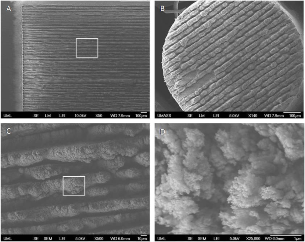
Figures 1(A) and (B) are SEM images of the fabricated quartz SERS surface and the optical fiber SERS endface, and depict a similar structure since the substrate and the fiber were made of the same material. The fs laser milled a single groove after finishing each scanning line, redepositing ablated fused silica material along the ridges between the grooves in the process. The structures created by this redeposited material were called micro-gratings. Figure 1(C) (boxed area inside Figure 1(A)) shows a magnified image of the ridges and grooves of these micro-gratings in the scanning area. Some ridges/grates overlapped with adjacent grooves. These overlapping areas showed nanometer-scale structures called nano-spikes because of the ablation and re-deposition of the material. Figure 1(D) shows the top view of a spot on one ridge (boxed area of Figure 1(C)), where nano-spikes, many less than 100 nm in size, can be clearly seen. When coated with silver, these unique nano-structures greatly enhance the Raman signal.
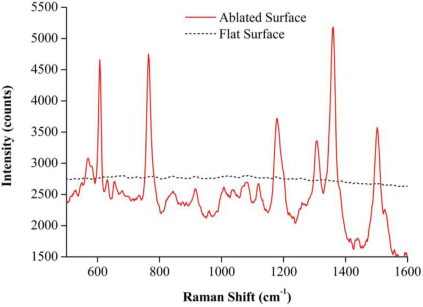
Figure 2 shows the spectrum of Rh6G solution (10−4 M concentration) measured on a flat reference surface coated with a 20 nm-thick layer of silver (dashed line), and compares it to the spectrum of a less concentrated Rh6G solution (10−7 M concentration) measured on the quartz SERS substrate/the fiber SERS probe (solid line). No Raman signal could be detected on the flat substrate, but characteristic signal peaks consistent with an enhanced SERS signal were detected on the two SERS substrates. The enhancement factor (EF) of the SERS signal can be estimated from Equation (1):
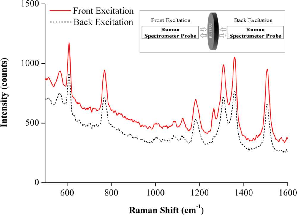
A promising way is to back excite the optical fiber SERS sensor for remote sensing applications. However, how to couple the Raman laser to the optical fiber well is a technique overcome. It is interesting to note that there was a slight decrease in the intensity of SERS signal when the detection was conducted on the back excited quartz SERS substrate via the excitation laser beam (Figure 3). In contrast, no any SERS signal was detected when the probe was back excited from the other end of the fiber by the excitation laser beam even after the length of the fiber was cut down to 10 cm. The phenomenon may have been caused by coupling losses between the Raman spectrometer’s probe and the optical fiber. Therefore, how to decrease coupling losses and improve SERS signal intensities would be one of focuses of the future work for remote sensing measurements.
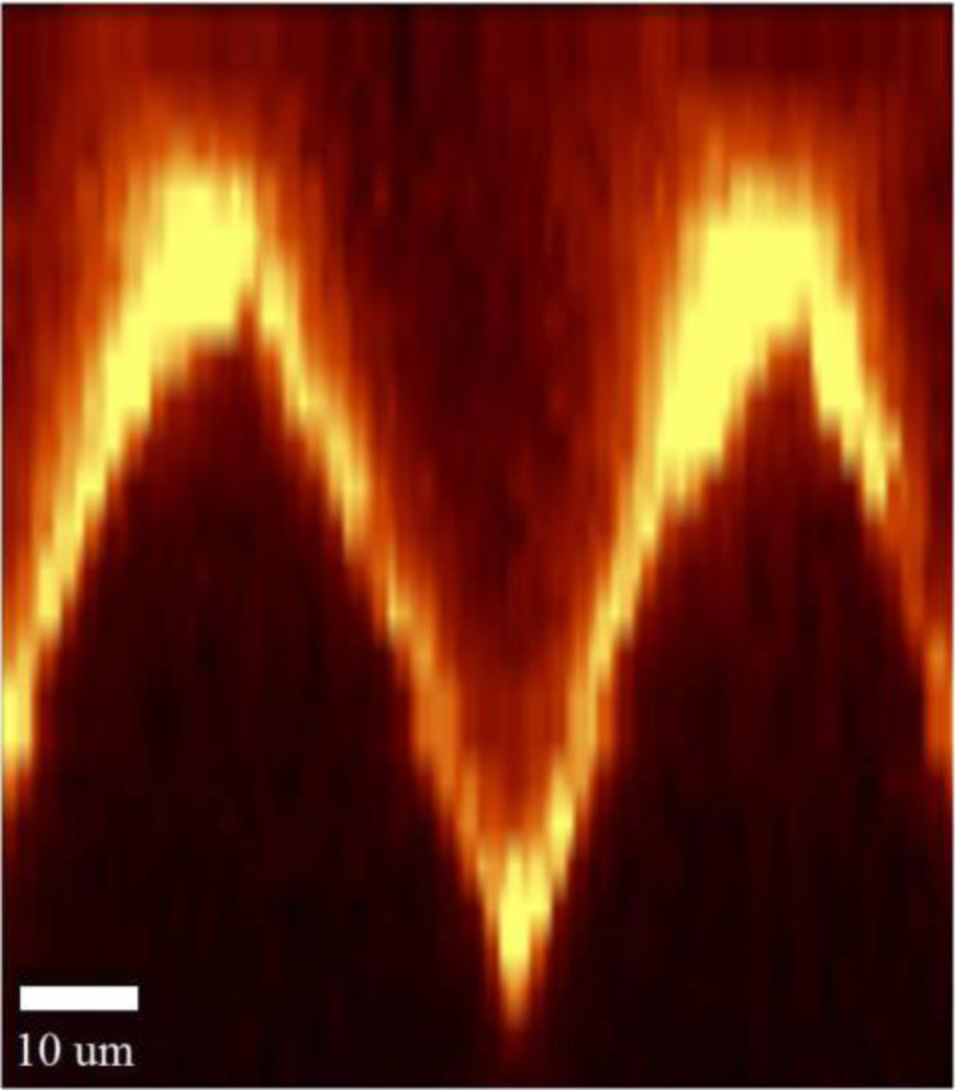
In order to better understand the profile of the micro-structure and how it related to signal enhancement, a confocal Raman microscope with a 532 nm excitation laser wavelength and 0.32 s integration time was used to take a Raman spectrum image of a cross section of the SERS substrates. The spectra were recorded with a linear 1,024 pixel CCD with a 600 g/mm grating. A Raman spectrum image of a cross-section of micro-gratings/grooves with Rh6G molecules was created by the integration of the total Raman intensity in an 85 μm by 100 μm scanning area, as shown in Figure 4. The variability in brightness indicates that the SERS signal intensity varied from position to position. Due to the way the silver evaporated during the thermal evaporation process, the ridge tops and the bottom grooves wound up being coated with more silver than the sloped areas. Consequently, the ridge tops and groove bottoms appeared brighter in the image than other areas of the substrate. More uniform silver deposition could be achieved by rotating or tilting the substrate during the silver deposition process.
5. Conclusions
An efficient fabrication method for optical fiber SERS probes through the fast fs laser scanning and the thermal evaporation of silver has been demonstrated. The effectiveness of SERS probes fabricated using this process was proved when the optical fiber probe detected a significantly enhanced Raman signal while measuring the spectrum of an Rh6G solution. The fs laser, with its speed, precision, and ability to operate in air, can therefore be used to make SERS probes and substrates in very small areas, such as inside chips and on optical fibers. Using an fs laser to make SERS sensors on the tips of optical fibers could provide an attractive sensing option for biological, chemical, and environmental remote sensing applications.
Acknowledgments
This multidisciplinary research work was supported by the Army Research Office under Contract No. W911NF-07-02-0081 and the National Science Foundation under Grant No. EEC-0425826a. The authors are grateful to Yoon Kim and Agiltron Inc. for their assistance with the Raman spectrum measurements, as well as Joey Mead, Carol Barry, and Julie Chen at the Nanomanufacturing Center at University of Massachusetts Lowell.
References
- Jeanmaire, DL; van Duyne, RP. Surface raman spectroelectrochemistry: Part I. Heterocyclic, aromatic, and aliphatic amines adsorbed on the anodized silver electrode. J Electroanal Chem 1977, 84, 1–20. [Google Scholar]
- Fleischmann, M; Hendra, PJ; McQuillan, AJ. Raman spectra of pyridine adsorbed at a silver electrode. Chem Phys Lett 1974, 26, 163–166. [Google Scholar]
- Mullen, KI; Carron, KT. Surface-enhanced Raman spectroscopy with abrasively modified fiber optic probes. Anal Chem 1991, 63, 2196–2199. [Google Scholar]
- Bello, JM; Vo-Dinh, T. Surface-enhanced Raman scattering fiber-optic sensor. Appl Spectrosc 1990, 44, 63–69. [Google Scholar]
- Zhang, Y; Gu, C; Schwartzberg, AM; Zhang, JZ. Surface-enhanced Raman scattering sensor based on D-shaped fiber. Appl Phys Lett 2005, 87, 123105:1–123105:3. [Google Scholar]
- Gu, C; Zhang, Y; Schwartzberg, AM; Zhang, JZ. Ultra-sensitive compact fiber sensor based on nanoparticle surface enhanced Raman scattering. In Photorefractive Fiber and Crystal Devices: Materials, Optical Properties, and Applications XI; SPIE: San Diego, CA, USA, 2005; pp. 591108–591166. [Google Scholar]
- Volkan, M; Stokes, DL; Vo-Dinh, T. Surface-enhanced Raman of dopamine and neurotransmitters using sol-gel substrates and polymer-voated fiber-optic probes. Appl Spectrosc 2000, 54, 1842–1848. [Google Scholar]
- Gessner, R; Rösch, P; Petry, R; Schmitt, M; Strehle, MA; Kiefer, W; Popp, J. The application of a SERS fiber probe for the investigation of sensitive biological samples. Analyst 2004, 129, 1193–1199. [Google Scholar]
- Stokes, DL; Vo-Dinh, T. Development of an integrated single-fiber SERS sensor. Sens Actuat B-Chem 2000, 69, 28–36. [Google Scholar]
- White, DJ; Stoddart, PR. Nanostructured optical fiber with surface-enhanced Raman scattering functionality. Opt Lett 2005, 30, 598–600. [Google Scholar]
- White, DJ; Mazzolini, AP; Stoddart, PR. Fabrication of a range of SERS substrates on nanostructured multicore optical fibres. J Raman Spectrosc 2007, 38, 377–382. [Google Scholar]
- Yi, Z; Gu, C; Schwartzberg, AM; Zhang, JZ. Single-fiber probe based on surface enhanced Raman scattering (SERS). Proceedings of IEEE Sensors 2005, Irvine, CA, USA, 31 October–3 November 2005; p. 4.
- Carmen, V; Wieland, H. Single-fibre surface-enhanced Raman sensors with angled tips. J Raman Spectrosc 2000, 31, 625–631. [Google Scholar]
- Lucotti, A; Zerbi, G. Fiber-optic SERS sensor with optimized geometry. Sens Actuat B-Chem 2007, 121, 356–364. [Google Scholar]
- White, IM; Gohring, J; Fan, X. SERS-based detection in an optofluidic ring resonator platform. Opt Express 2007, 15, 17433–17442. [Google Scholar]
- Kostovski, G; White, DJ; Mitchell, A; Austin, MW; Stoddart, PR. Nanoimprinted optical fibres: Biotemplated nanostructures for SERS sensing. Biosens Bioelectron 2009, 24, 1531–1535. [Google Scholar]
- Shen, MY; Crouch, CH; Carey, JE; Mazur, E. Femtosecond laser-induced formation of submicrometer spikes on silicon in water. Appl Phys Lett 2004, 85, 5694–5696. [Google Scholar]
- Gattass, RR; Mazur, E. Femtosecond laser micromachining in transparent materials. Nat Photonics 2008, 2, 219–225. [Google Scholar]
- Diebold, ED; Mack, NH; Doorn, SK; Mazur, E. Femtosecond laser-nanostructured substrates for surface-enhanced Raman scattering. Langmuir 2009, 25, 1790–1794. [Google Scholar]
- Zhou, Z; Xu, J; Cheng, Y; Xu, Z; Sugioka, K; Midorikawa, K. Surface-enhanced Raman scattering substrate fabricated by femtosecond laser direct writing. Jpn J Appl Phys 2008, 47, 189–192. [Google Scholar]
- Han, Y; Lan, X; Wei, T; Tsai, HL; Xiao, H. Surface enhanced Raman scattering silica substrate fast fabrication by femtosecond laser pulses. Appl Phys A Mater Sci Process 2009, 97, 721–724. [Google Scholar]
- Lan, X; Han, Y; Wei, T; Zhang, Y; Jiang, L; Tsai, H-L; Xiao, H. Surface-enhanced Raman-scattering fiber probe fabricated by femtosecond laser. Opt Lett 2009, 34, 2285–2287. [Google Scholar]
- van Duyne, RP; Hulteen, JC; Treichel, DA. Atomic force microscopy and surface-enhanced Raman spectroscopy. I. Ag island films and Ag film over polymer nanosphere surfaces supported on glass. J Chem Phys 1993, 99, 2101–2115. [Google Scholar]
- Baia, M; Baia, L; Astilean, S; Popp, J. Surface-enhanced Raman scattering efficiency of truncated tetrahedral Ag nanoparticle arrays mediated by electromagnetic couplings. Appl Phys Lett 2006, 88, 143121–143123. [Google Scholar]
- Kudelski, A. Raman studies of rhodamine 6G and crystal violet sub-monolayers on electrochemically roughened silver substrates: Do dye molecules adsorb preferentially on highly SERS-active sites. Chem Phys Lett 2005, 414, 271–275. [Google Scholar]
- Santesson, S; Johansson, J; Taylor, LS; Levander, I; Fox, S; Sepaniak, M; Nilsson, S. Airborne chemistry coupled to Raman spectroscopy. Anal Chem 2003, 75, 2177–2180. [Google Scholar]


© 2010 by the authors; licensee MDPI, Basel, Switzerland. This article is an open access article distributed under the terms and conditions of the Creative Commons Attribution license ( http://creativecommons.org/licenses/by/3.0/).
Share and Cite
Ma, X.; Huo, H.; Wang, W.; Tian, Y.; Wu, N.; Guthy, C.; Shen, M.; Wang, X. Surface-Enhanced Raman Scattering Sensor on an Optical Fiber Probe Fabricated with a Femtosecond Laser. Sensors 2010, 10, 11064-11071. https://doi.org/10.3390/s101211064
Ma X, Huo H, Wang W, Tian Y, Wu N, Guthy C, Shen M, Wang X. Surface-Enhanced Raman Scattering Sensor on an Optical Fiber Probe Fabricated with a Femtosecond Laser. Sensors. 2010; 10(12):11064-11071. https://doi.org/10.3390/s101211064
Chicago/Turabian StyleMa, Xiaodong, Haibin Huo, Wenhui Wang, Ye Tian, Nan Wu, Charles Guthy, Mengyan Shen, and Xingwei Wang. 2010. "Surface-Enhanced Raman Scattering Sensor on an Optical Fiber Probe Fabricated with a Femtosecond Laser" Sensors 10, no. 12: 11064-11071. https://doi.org/10.3390/s101211064