Metal-Insulator-Semiconductor Photodetectors

1
Institute of Opto-Electronic Engineering, National Dong Hwa University, Hualien 97401, Taiwan
2
Department of Electrical Engineering, Graduate Institute of Electronics Engineering, and Graduate Institute of Photonics and Optoelectronics, National Taiwan University, Taipei 10617, Taiwan
*
Author to whom correspondence should be addressed.
Sensors 2010, 10(10), 8797-8826; https://doi.org/10.3390/s101008797
Submission received: 5 August 2010
/
Revised: 7 September 2010
/
Accepted: 14 September 2010
/
Published: 28 September 2010
(This article belongs to the Special Issue Photodetectors and Imaging Technologies)
Abstract
:The major radiation of the Sun can be roughly divided into three regions: ultraviolet, visible, and infrared light. Detection in these three regions is important to human beings. The metal-insulator-semiconductor photodetector, with a simpler process than the pn-junction photodetector and a lower dark current than the MSM photodetector, has been developed for light detection in these three regions. Ideal UV photodetectors with high UV-to-visible rejection ratio could be demonstrated with III–V metal-insulator-semiconductor UV photodetectors. The visible-light detection and near-infrared optical communications have been implemented with Si and Ge metal-insulator-semiconductor photodetectors. For mid- and long-wavelength infrared detection, metal-insulator-semiconductor SiGe/Si quantum dot infrared photodetectors have been developed, and the detection spectrum covers atmospheric transmission windows.
1. Introduction
Photo-detection ranging from ultraviolet (UV) through the visible to infrared (IR) regions is closely related to human life. UV light is usually divided into three regions: UV-A, UV-B, and UV-C [1]. UV-C (10 nm–280 nm) light has the largest photon energy among the three UV regions, and hence, it is the most harmful to human beings. However, most of it is absorbed by the atmospheric ozone layer. UV-B (280 nm–320 nm) can partially pass through the atmospheric ozone layer, and can lead to skin cancer. UV-A (320 nm–400 nm) has the smallest photon energy and causes less harm for people. UV photodetectors can provide early warning signs for preventing overexposure. Detection of UV light can also be used in chemical and biological analysis. Visible light covers the range of wavelengths from 400 nm to 700 nm. Human eyes are natural visible photodetectors. In order to reproduce surrounding sights, visible photodetectors are significant. Beyond the visible wavelengths, a broad range of wavelengths constitute the infrared region. The detection of infrared can be roughly divided into two groups: for wavelengths shorter than 2 μm, known as the near-infrared region, the detection can be used for telecommunications and optical interconnects. For wavelengths longer than 2 μm, corresponding to the mid- and long-wavelength infrared, the detection can be used for imaging systems in astronomy, military, medicine, and other applications [2,3].
The common types of photodetectors include p-i-n, metal-semiconductor-metal (MSM), and metal-insulator-semiconductor (MIS) structures [4,5]. When an intrinsic semiconductor is sandwiched between a highly doped p-type layer and a highly doped n-layer, we have the basic configuration of a p-i-n type detector. A built-in electric-field will be formed inside the whole structure. A reversed bias could enlarge this electric field. When a target light with a suitable wavelength irradiates this structure, electron-hole pairs could be generated and separated by the electric field. Photo-detection can be achieved with such a mechanism. The MSM detector has a similar photo-detection principle, with the electric field distributed inside the semiconductor region. For the MIS detector, an insulator layer is inserted between the metal and semiconductor. A thin insulator layer in the MIS structure can allow a significant tunneling gate current, which could be utilized for photodetectors. A deep-depletion region formed in the semiconductor of the MIS detector can provide the electric field for separation of photo-generated electron-hole pairs. Compared to p-i-n detectors, MIS detectors offer a simpler process since the doping of PIN detectors is usually accomplished via implantation or diffusion. Since a thin insulator layer is between the metal and semiconductor, the dark currents of MIS detectors can usually be lower than those of MSM detectors. The extra surface barrier and decrease of interface states can contribute to the reduction of dark currents [6].
This review focuses on MIS photodetectors working in the UV, visible or infrared regions. First, the electrical characteristics of the MIS structure will be discussed. The MIS UV photodetectors using wide-bandgap semiconductor materials or metal filters will be discussed in Section 3. Then, the MIS structures for visible-to-near-IR detection employing the most broadly used semiconductor material, Si, will be discussed. Ge can be used to extend the cutoff wavelength of Si photodetectors. Finally, mid- and long-wavelength infrared detection by HgCdTe MIS photodetectors and MIS SiGe/Si quantum dot (well) infrared photodetectors will be introduced in Section 5.
2. Electrical Characteristics of MIS Structures
MOSFETs have become basic components of most electronic devices. In order to increase circuit performance, the quest to scale down MOSFETs continues. As the device size is scaled down, the oxide thickness decreases and the gate tunneling current along the vertical MOS structure (in the special case of MIS structures) then increases. Figure 1 shows the relation between the gate tunneling current and oxide thickness [7,8].
Figure 1 indicates that the direct tunneling current of the MOS structure with high-quality thermal oxide gradually becomes significant when the oxide thickness is less than 3 nm. For low-quality oxide, such as liquid-phase-deposition oxide, the current becomes significant even at a larger thickness with the help of trap-assisted tunneling.
As a photodetector, MOS diodes are usually operated at the inversion bias. For example, a positive bias should be applied on the Al/SiO2/p-Si diode for light detection. From [8], the dark current density J via the tunneling process of direct tunneling for the vertical MOS diode with an MOSFET transistor structure can be simplified as:
with:
and at the inversion bias, the carrier density N(Vg) can be approximated as:
where:
| A, B, D, and α | model parameters; |
| Tox | oxide thickness; |
| Vox | oxide voltage; |
| φb0 | semiconductor/oxide barrier height; |
| φb | actual tunneling barrier height; |
| Vth | threshold voltage. |
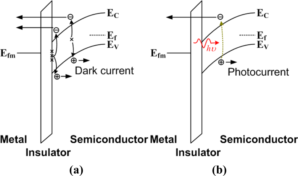
Equation (2) shows that M(Vox) is a complicated function of Vox. The magnitude of M(Vox) will increase as Vox increases in the regions of interest. The “NMOS of NMOSFET” curve in Figure 2(a) indicates that Vox of an NMOS diode with a transistor structure is a linear function of the gate voltage (Vg). In addition, the Vg/Tox term and N(Vg) term in Equation (1) also contribute to the increase of the direct tunneling current density J as Vg increases. Overall, the direct tunneling current density of an NMOS diode with a transistor structure shows an exponential-like behavior as Vg increases (“NMOS of NMOSFET” curve in Figure 2(b)). On the other hand, the NMOS diode without a transistor structure is quite different. At the inversion bias, inversion carriers cannot be supplied from the source and drain of an MOSFET transistor. This results in the soft pinning of Vox as Vg increases (“NMOS only” curve in Figure 2(a)) [9]. In addition, the inversion carrier density will not be Vg dependent as shown in Equation (3). Therefore, the dark direct tunneling current of an NMOS diode without a transistor structure is relatively constant in the log scale (“NMOS only” curve in Figure 2(b)). This dark inversion current density is dominated by the minority-carrier (electrons in p-Si, for example) generation rate at the oxide/semiconductor interface and in the deep-depletion region of the semiconductor (Figure 3(a)). For detector applications, an MIS diode without a transistor structure is preferred. Hence, the following discussion of MIS photodetectors will focus on those without transistor structures. Gate tunneling currents in MIS diodes without transistor structures have been comprehensively studied in [10].
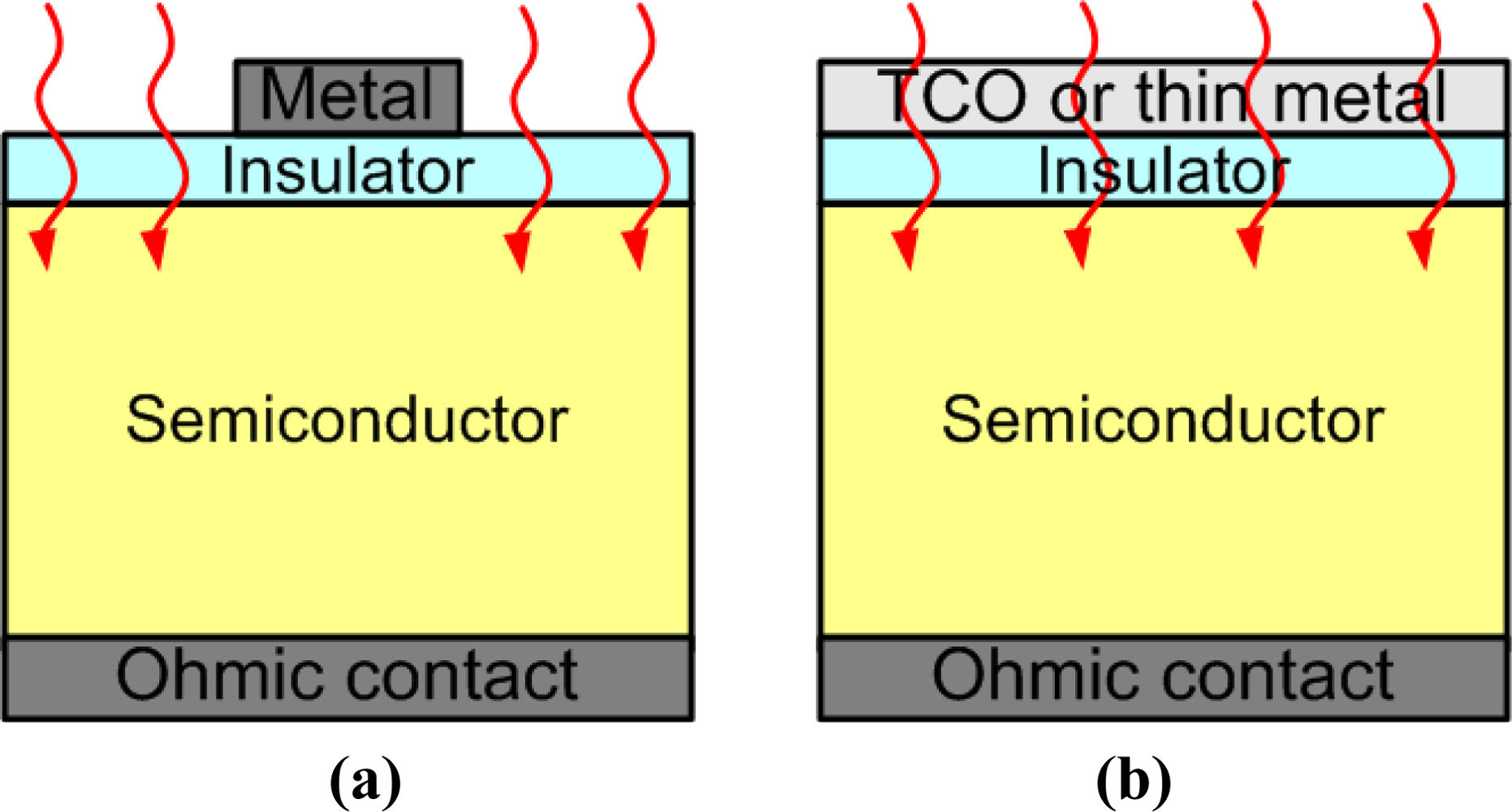
Under light exposure at the inversion bias, excess electron-hole pairs are generated in the semiconductor and contribute to the photocurrent (Figure 3(b)). For the MIS photodetector with a nontransparent metal gate, the incident light is incorporated into the semiconductor from the edge of the metal gate (Figure 4(a)). In order to increase the responsivity of a photodetector, a transparent gate could be utilized, and the incident light would be incorporated into the semiconductor directly from the gate (Figure 4(b)). Transparent gates can be roughly classified into two categories. The first are the transparent conducting oxides (TCOs), such as indium tin oxide (ITO) or zinc oxide (ZnO). The other are the metal films with thicknesses of ∼10 nm [11]. Since the metal film is so thin, absorption of the incident light in the metal is suppressed.
The thickness of the insulator layer will influence both the dark currents and photocurrents of the MIS photodetectors. A thicker insulator results in smaller currents. For example, Monroy et al. have discussed the effects of the SiO2 thickness on GaN MIS photodetectors [12]. When the thicknesses of SiO2 was varied from 2.5 nm to 5 nm, the corresponding dark current densities (at −2 V) varied from ∼7 × 10⁻⁵ to 4 × 10⁻⁶ A/cm2, and the corresponding photocurrents (at 100 W) varied from ∼0.7 to 0.09 A, respectively. Meanwhile, the dark current density and photocurrent of a Schottky barrier GaN photodiode were ∼8 × 10⁻⁴ A/cm2 and 5 A. The thicker insulator could be used for lower noise operation, but the trade-off is the lower responsivity.
The speed of a photodetector may be limited by the carrier transit time or RC delay. If the photodetector is transit time limited, the bandwidth is given by [13]:
where W is the width of the depletion region, and vs is the saturation velocity. The term vs is a material-dependent parameter. In the deep-depletion situation, the W of an MIS diode can be approximated as [14]:
where N is the doping concentration of the semiconductor. With Equations (4) and (5), the transit time limited bandwidth can be determined. If the photodetector is RC delay limited, the bandwidth will be [15]:
where R includes the series resistance and load resistance. The C of an MIS photodetector is dominated by the semiconductor depletion capacitance in series with the insulator capacitance [16]. When the order of ftransit is close to that of fRC, the resultant f should be [15]:
3. MIS UV Photodetectors
Applications of UV detection include chemical monitoring, biological sensing, missile plume detection, exposure monitoring, etc. The wide-bandgap semiconductor is suitable for UV detection when visible light will not contribute to the absorption [17]. The wide-bandgap III–V nitride, SiC, and Zn-based semiconductor MIS UV photodetectors will be discussed. Si, which has a much smaller bandgap than the III–V nitride semiconductor, is a strong absorber for UV light. A Si MIS structure with an appropriate selection of the gate electrode can also be used for UV detection.
3.1. III–V MIS UV Photodetectors
The III–V nitride semiconductors, (Al, In, Ga)N, are direct bandgap materials. The absorption edge of AlN is 200 nm, and the absorption edge of GaN is 365 nm [18]. Using (In, Ga)N alloys, the absorption edge can be extended to 400 nm. With varying Al mole fraction in (Al, In, Ga)N alloys, the detection edge can be tuned. These III–V nitride materials can be fabricated into simple MIS photodetectors. Compared with metal-semiconductor (Schottky barrier) photodiodes, insertion of a thin SiO2 layer for the III–V nitride photodetector can effectively decrease the dark current. For example, Monroy et al. have demonstrated the dark current reduction with the Au/SiO2/GaN MIS photodetector [16]. The magnitude of the dark current of the Au/SiO2/GaN MIS photodetector is four orders lower than the Au/GaN Schottky photodetector, and the noise spectral density of the MIS photodetector is also three orders lower than the Schottky photodetector due to the passivation by SiO2
Since GaN is a well-known III–V nitride material, the study on the GaN MIS UV photodetector will be very representative. Two GaN MIS UV photodetectors based on different techniques of insulator formation by different groups will be introduced here, and the results show that similar performances could be achieved. (I) A GaN MIS UV photodetector with a photo chemical-vapor-deposition (photo-CVD) SiO2 layer was studied by Chiou et al. [19]. The deuterium (D2) lamp was selected as a photo-CVD photo excitation source. The D2 lamp could effectively decompose reacting gas, and it resulted in a high quality SiO2 layer. The SiO2 film was 50 nm thick. The high frequency capacitance-voltage measurement showed that the Dit between SiO2 and GaN could be as low as 8.4 × 1011 cm−2 eV−1. Such a low Dit was believed to be due to effective decomposition by the D2 lamp. The low Dit was proved to lead to a low leakage current. As compared with the photodiode without the SiO2 film, the dark current was decreased by seven orders while the photocurrent was only decreased by four orders. Hence, the final photocurrent to dark current ratio was increased by three orders. The normalized detectivity (D*) was defined as [20]:
where A is the area of the investigated photodetector, and Δf is the bandwidth of the photodetector. The noise equivalent power (NEP) was formulated as in/R, where in is the current noise and R is the responsivity. The difference between the photocurrent and dark current was divided by the input power to obtain the responsivity. The responsivity of a photodetector should be as large as possible. This ITO/photo-SiO2/GaN had a responsivity of ∼120 mA/W. The NEP was estimated to be 2.2 × 10⁻⁹ W. With a detector size of 200 × 200 μm2 and given bandwidth of 500 Hz, the normalized detectivity was calculated using Equation (8) to be 2.0 × 108 cm Hz0.5W−1.
(II) Hwang et al. also demonstrated a GaN MIS UV photodetector with a liquid-phase-deposition (LPD) SiO2 layer [21]. LPD is a low-temperature (30 °C–40 °C) process, which could prevent the redistribution of concentrations at a high temperature. The deposited SiO2 could be annealed at 800 °C in order to achieve a denser film. The minimum Dit of this LPD-SiO2 device was the same (8.4 × 1011 cm−2 eV−1) as the photo-SiO2 device just mentioned. The responsivity of the 10 nm thick LPD-SiO2 MIS photodetector at the 366 nm wavelength was 112 mA/W, which was also close to the result of the photo-SiO2 photodetector. It should be noted that since the oxide was 10 nm thick, carriers could hardly tunnel through the oxide layer via the mechanism of direct tunneling. Hwang et al. indicated that defect-assisted tunneling might help the carrier transport. Although the normalized detectivity of this Al/LPD-SiO2/GaN MIS UV photodetector was not given, its detectivity could be estimated as follows: as discussed in [20], the in (V ≠ 0) could be approximated as the shot noise (2eIdΔf)1/2, where Id was the dark current of the photodetector. Therefore, D*; in Equation (8) could be simplified as:
In Equation (9), the A/Id term corresponds to the reciprocal of the dark current density. It could be found that the dark inversion (depletion) current densities of ITO/photo-SiO2/GaN in [19] and Al/LPD-SiO2/GaN in [21] were of the same order of magnitude. Since the responsivities of both devices are close, the normalized detectivities would be at the same order, too.
The most common source of UV light is the Sun, which also radiates visible light. In order to indicate the UV intensity, the development of visible-blind UV photodetectors is important [22]. The characteristics of three different structures (Figure 5) of AlGaN/GaN photodetectors have been compared, and the MIS photodetector was found to have a higher UV-to-visible rejection ratio as compared with the MSM photodetector [23].
First, on the AlGaN/GaN sample, two inter-digitated Pt contacts were deposited to form the MSM photodetector (Figure 5(a)). If a 5 nm thick photo-CVD SiO2 layer could be deposited before the deposition of Pt gates, an un-optimized MIS photodetector was able to be formed (Figure 5(b)). Another 50 nm thick SiO2 deposited between two inter-digitated contacts achieved the optimized MIS photodetector with anti-reflection (AR) coating (Figure 5(c)). Due to the passivation of the 50 nm thick SiO2 layer in the MIS photodetector with AR coating, the reduced surface states resulted in the lowest dark current among these three photodetectors. On the other hand, the photocurrent of the MIS photodetector with AR coating was larger than the MIS photodetector without AR coating since the reflection of the incident light could be suppressed. In addition, the passivation of 50 nm thick SiO2 could also reduce the recombination of photo-generated carriers. The resultant spectral responsivities of these three photodetectors were shown in Figure 6. The UV-to-visible rejection ratio of the MIS photodetector with AR coating was the largest, and the ratio was more than three orders of magnitude.
Some typical III–V nitride based UV photodetectors with different configurations are compared in Table 1. The dark current densities are shown for reference. However, as discussed in [26], the uncertainty of the junction area makes the direct comparison of current densities confusing. If the compared devices are fabricated into similar structures, the comparison would be much meaningful. For example, MIS and MSM AlGaN/GaN photodetectors in [23] show that the insertion of an insulator layer indeed reduces the dark current densities. From this table, we can still conclude that the p-i-n type photodetectors have the potential to achieve the lowest dark current densities.
3.2. SiC MIS UV Photodetectors
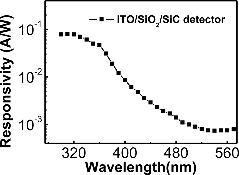
SiC is also a wide-bandgap material, which can be used for UV photo-detection. The SiC pn junction photodiodes and Schottky barrier (SB) photodiodes have been well developed [30]. A 4H-SiC MIS photodetector with a photo-CVD SiO2 layer was also fabricated [31]. The Dit between SiC and photo-CVD SiO2 deposited at 150, 300, and 500 °C was 3.3 × 10¹², 3.2 × 10¹², and 5.7 × 1011 cm−2 eV−1, respectively. The higher temperature was able to provide more thermal energy for photo-decomposition of SiH4 and O2 gases, which resulted in a better SiO2/SiC interface. The surface morphology of a bare SiC substrate and a substrate with a photo-CVD SiO2 layer were studied by atomic force microscopy (AFM). The AFM showed that the root-mean-square roughness of surfaces without and with SiO2 layers were 0.32 and 4.24 nm, respectively. Although the substrate with an SiO2 layer had a rougher surface, its electrical characteristics do not reveal obvious disadvantages. The ITO/SiO2/SiC MIS photodetector was compared with an ITO/SiC SB photodetector. At 10 V, the dark current densities of MIS and SB detectors were 1.3 × 10⁻⁶ and 1.1 × 10⁻³ A/cm2, respectively. Both the dark current and photocurrent of the ITO/SiO2/SiC MIS detector were smaller than those of the ITO/SiC SB detector. Overall, the photocurrent to dark current ratio of the ITO/SiO2/SiC MIS detector was still much larger than that of the ITO/SiC SB detector. The spectral responsivity of the ITO/SiO2/SiC MIS detector was studied as shown in Figure 7. The UV-to-visible rejection ratio was ∼80, which was much lower than that of AlGaN/GaN MIS detector with AR coating as discussed in the previous subsection. A high performance 4H-SiC p-i-n UV photodetector was demonstrated by Chen et al. with a UV-to-visible rejection ratio larger than 103 [32]. Much effort should be done to improve the rejection ratio of MIS detectors to compete with p-i-n ones.
3.3. Zn-Based MIS UV Photodetectors
Some II–VI semiconductor, like ZnSe, is a promising wide-bandgap material, too. The bandgap of ZnSe is about 2.6 eV [33]. ZnSe MIS photodetectors with different insulator layers have been investigated, including SiO2 and Ba0.25Sr0.75TiO3 (BST) [34]. With the insertion of an SiO2 layer or a BST layer, the dark currents decreased more than one order of magnitude as compared with ZnSe SB photodetectors. The UV (400 nm)-to-visible (500 nm) rejection ratio were about 120, 50, and 10 for ITO/SiO2/ZnSe, ITO/BST/ZnSe, and ITO/ZnSe photodetectors, respectively. The corresponding detectivities were 2.55 × 10¹², 1.67 × 10¹², and 1.5 × 10¹¹ cmHz0.5W−1. The MIS structure was desirable for ZnSe UV photodetectors.
The superiority of the MIS structure over the MSM structure has also been shown for the material of ZnO, which has the bandgap of 3.37 eV [35]. For ZnO, the shortcomings of a pn-junction-type photodetector include not only the process complexity, but also the difficulty on formation of p-type ZnO [36]. The reproducibility and reliability of ZnO p-i-n photodetectors will be the issues. Hence, an MIS structure of ZnO is very favorable for photodetector applications. The test structures were very similar to the MSM detector and MIS detector without AR coating shown in Figure 5, and the probably optimized structure of the MIS detector with AR coating was not yet presented. Nevertheless, the high UV (370 nm)-to-visible (450 nm) rejection ratio of 3.8 × 10³ of this ZnO MIS photodetector was still larger than that of 2.4 × 10² of the ZnO MSM photodetector. The quite low long-wavelength responsivity of this MIS detector contributed to its excellent rejection ratio.
Furthermore, a derivative of ZnO, MgZnO, was fabricated into an Au/MgO/MgZnO MIS photodetector [37]. Such an Au/MgO/MgZnO photodetector possessed a high internal gain, and hence it is worthy of mention here. The MgZnO semiconductor film was deposited on the sapphire substrate by the metal-organic chemical vapor deposition technique. Subsequently, an MgO insulator layer was deposited by the sputtering technique. Finally, a 20 nm thick Au gate on the MgO layer and a ring-shaped Al contact on the MgZnO were deposited to form the MIS photodetector. For comparison, a metal-semiconductor photodetector without the MgO insulator film was also prepared. The responsivity versus applied voltage curves displayed interesting behaviors (Figure 8). The responsivity of the MIS photodetector increased exponentially with the increasing bias, meanwhile the MS photodetector showed a typical linear behavior [38,39].
The estimated external quantum efficiencies of the MIS and MS photodetectors were 22% and 0.26% at 5 V, respectively. The external quantum efficiency of the MIS photodetector increased to 200% at 21 V. The excellent results of the MIS photodetector came from the optical gain through the impact ionization process. Figure 9 shows the mechanism of optical gain in the MIS photodetector. When the UV light irradiated to the MgZnO semiconductor, electron-hole pairs could be generated. Photo-generated holes drifted toward the Au contact through the MgO insulator layer. These holes gained much kinetic energy in the trip, and extra electron-hole pairs were then generated via the impact ionization process. This multiplication process contributed to the exponential increase on the responsivity as a function of the applied voltage.
3.4. Metal-Filter Si MIS UV Photodetectors
Si is a strong absorber of UV light. For example, the absorption length at the 320 nm wavelength is below 10 nm in Si. The typical Si UV photodetectors are classified into two categories [30]. One are the diffused photodiodes with depletion regions between the p and n layers. The other is the SB photodiodes with depletion regions at the metal/semiconductor interfaces. Applications of UV detection based on Si are usually limited since Si has a broadband absorption for the solar spectrum. A visible-blind design for the Si UV photodetector is desirable. Ho et al. have demonstrated a Si MIS UV photodetector using Ag as the filter [40]. A ∼3 nm thick SiO2 layer was grown on an n-type Si wafer by rapid thermal oxidation. After oxidation, the Ag gate was deposited for band selection of UV light. Al was then evaporated on the backside of the Si wafer to form an Ohmic contact. The schematic structure of the Si MIS UV photodetector is shown in Figure 10. Incident photons were firstly selected by the Ag gate, and then the remaining photons might be absorbed by Si to generate electron-hole pairs. These photo-generated electron-hole pairs in Si were separated by the electric field in the depletion region. Since the absorption length of the UV light in Si was very short, the depletion region should be as close to the incident surface as possible. As compared to the p-i-n structure, the MIS structure could have the depletion region closer to the surface. In principle, the MIS photodetector would achieve the higher quantum efficiency [41].
When the thicknesses of Ag gates were varied from 70 to 130 nm, the peaks of the spectral responsivities were still located at the wavelength of 319 nm, with values of 17.3 to 5.1 mA/W (Figure 11). The transmission of UV band at the ∼319 nm wavelength was due to the material property of Ag (spectral dependence of absorption and reflection). The full width at half magnitude (FWHM) decreased as the thickness of Ag increased too. The FWHM decreased from 17 to 11 nm when the thickness of Ag was varied from 70 to 130 nm. Although the UV-to-visible rejection ratio of the metal-filter Si MIS photodetector was smaller than the AlGaN/GaN MIS photodetector mentioned in Subsection 3.1, a smaller FWHM could be achieved with such a photodetector.
4. MIS Visible-to-Near-IR Photodetectors
The spectral distribution of terrestrial solar radiation shows that the visible band has the largest intensity. Creatures, including human beings, on the surface of Earth, are the most sensitive to the visible light, therefore, the development of visible photodetectors is important. Si is the most promising material for visible detection since it has a suitable bandgap (1.12 eV) for visible-light absorption and it is one of the most abundant materials on Earth. Si can also detect the useful near infrared at the 850 nm wavelength. Near infrared has many significant applications, such as optical interconnects and optical communications [42]. In order to extend the detection wavelength to the other useful near-infrared bands of ∼1.3 and 1.55 μm, Ge, which is compatible with the mature Si process, is utilized. Representative MIS structures for visible or near-infrared photodetectors are introduced in this section.
4.1. Si-Based MIS Visible-to-Near-IR Photodetectors
Si-based MIS photodetectors are desirable due to the probability of integration with ULSI circuits. The photocapacitive mode MIS photodetector was proposed in 1980 [43], and optical sensors based on transient behaviors in MIS-capacitors were discussed by Malik et al. in 2004 [44,45]. However, MIS photodetectors using tunneling-photocurrent mode are more broadly used [46–49]. First, the simple NMOS and PMOS Si tunnel diodes will be introduced. The ultrathin (2.3 and 2.7 nm) oxide layers were grown by rapid thermal oxidation on the 1–5 cm p-type and n-type Si wafers in order to form the NMOS and PMOS tunneling diodes, respectively [9,50].
The J-V curves of the NMOS and PMOS photodetectors are shown in Figures 12(a) and 12(b), respectively. A metal halide lamp was used to excite the photocurrents. The dark current and photocurrents of the NMOS photodetector remained almost constant in the log scale when the positive bias was applied. Thermally generated electron-hole pairs at the SiO2/p-Si interface and in the depletion region in p-Si contributed to the dark current. With light exposure, the generation rate of electron-hole pairs increased and thus the gate tunneling current increased. For such ultrathin SiO2, the tunneling rate here was not a limiting factor for electrons tunneling from the p-Si to the Al gate, and hence these currents could keep almost constant with increased biases. Figure 12 shows the photocurrents under different light intensity. If ITO was used instead of Al as the gate electrode, the magnitude of the photocurrent could be increased by a factor of 20 [9].
The mechanism of the photocurrent in the PMOS photodetector was a little more complicated. A kink appeared in the photocurrents but not in the dark current. The first plateau of the photocurrent was also due to the excess electron-hole-pair generation with light exposure. The second plateau was due to the electron direct tunneling from the Al gate to n-Si (Figure 13). The hole concentration at the SiO2/n-Si interface was determined by the tunneling rate and photo-generation rate of holes. As the negative bias continuously increased, hole concentration at the interface increased, and the oxide voltage increased slightly. The Fermi level of Al would arise away from the level of the conduction band edge of n-Si at the SiO2/n-Si interface, and the electron direct tunneling from the Al gate to n-Si occurred. Hence, there was a second plateau of the photocurrent. A similar phenomenon was observed by Hashimoto et al. [51].
In the above design, the gate electrodes and back Ohmic contacts were on different sides of the Si substrates. Both electrodes could be formed on the same side of thin-oxide/Si substrates to fabricate interdigitated metal-insulator-semiconductor-insulator-metal (MISIM) photodetectors (Figure 14) [45,52]. Such a structure could be compared with the MSM structure with the same metal pattern, and then the advantages of the insertion of an insulator layer became obvious. Seto et al. showed that the insertion of a thin SiO2 layer effectively reduced the dark current by a factor of 5.2 [52]. The increase in the dark current with the increasing bias was weaker. Furthermore, the responsivity was increased by a factor of 3.5 with such an MISIM structure. The responsivity measurement was operated under 635 nm laser diode illumination. At 5 V, the responsivities of the MISIM and MSM photodetectors were 0.39 and 0.11 A/W, respectively. In addition, the internal quantum efficiency of the MISIM detector was shown to be 1.8 larger than 0.5 of the MSM detector. There might be holes trapped at the insulator/semiconductor interface. These holes induced an additional electron tunneling current, which made the internal quantum efficiency of the MISIM detector larger than unity.
Due to the Si bandgap, the near infrared at the optical communication wavelengths of 1,300 and 1,550 nm cannot be detected. The detection performance at the wavelength of 820 nm is also limited. Five periods of SiGe quantum-dot layers were incorporated into the Si substrate to improve the near-infrared performance of MIS photodetectors [53]. The SiGe/Si quantum dots were grown on the Si substrate by the ultrahigh vacuum chemical vapor deposition with the Stranski-Krastanov growth mode. The SiGe layer acted as a low-bandgap region, which enhanced the absorption coefficient and extended the cut-off wavelength as compared with the Si device. The responsivities of the MIS SiGe/Si quantum-dot photodetector at wavelengths of 820, 1,300, and 1,550 nm were 130, 0.16, and 0.08 mA/W, respectively. If the number of periods of SiGe quantum-dot layers was increased to 20, a responsivity of 600 mA/W could be achieved at the wavelength of 850 nm.
4.2. Bulk Ge MIS Visible-to-Near-IR Photodetectors
As mentioned in the previous subsection, Ge can be used for detection of near infrared at the 1,300 and 1,550 nm wavelengths. Ge photocapacitive mode MIS infrared photodetectors were proposed in 1979 [54]. In order to demonstrate the tunneling-photocurrent mode Ge MIS photodetector, a thin SiO2 layer was formed on the Ge substrate with the process of low-temperature liquid phase deposition (LPD) [55]. Note that the insulator layer was SiO2 instead of GeO2 since GeO2 was unstable and had a worse quality. The detailed LPD process flow is shown in Figure 15 [53].
In [55], Ge MIS structures were both used as photodetectors and light-emitting diodes (LEDs). The Ge MIS structure with an inversion bias acted as a photodetector, while it acted as an LED with an accumulation bias. The responsivities of the bulk Ge MIS photodetector at wavelengths of 1,310 and 1,550 nm were 180 and 53 mA/W, respectively. The data communication in free space has been demonstrated using a Ge MIS photodetector and a Ge MIS LED (Figure 16).
The function generator was used to modulate the Ge MIS LED. Then, emission from the Ge MIS LED was detected by the Ge MIS photodetector. Finally, the corresponding photocurrent was read from the output instrument. The results of the data communication of this system are shown in Figure 17. When the modulation frequency is 300 Kbit/s, both the light intensity of the Ge MIS LED and the photocurrent of the Ge MIS photodetector followed the modulated input current. When the modulation frequency was as high as 15 Mbit/s, a delay time of ∼19 ns was observed between the light intensity of the Ge MIS LED and the photocurrent of the Ge MIS photodetector. The bandwidth of this Ge MIS photodetector was estimated to be ∼300 MHz. Hence, the modulation frequency for this free space data communication was limited by this Ge MIS photodetector. Optimized structures with, such as a small active area or a high-quality oxide layer without trapping would be needed to increase the modulation frequency.
A suitable selection of the metal in the metal/SiO2/n-Ge photodetector may reduce the dark current which then improves the signal-to-noise ratio. In Figure 13, a mechanism of electron direct tunneling under light exposure was studied. Such an electron direct tunneling also contributed to the dark current. If the high-work-function metal was used, the dark current could be decreased with the suppression of electron tunneling from the metal to n-Ge. Dark inversion current reduction has been achieved with the high-work-function metal, Pt (5.65 eV), instead of the typical low-work-function metal, Al (4.1 eV) for Ge MIS photodetectors (Figure 18) [56].
4.3. Thin-Film Ge MIS Visible-to-Near-IR Photodetectors
The bulk Ge photodetector can detect the infrared at wavelengths of 1,310 and 1,550 nm, but the cost and the device speed are issues. Thin-film Ge photodetectors can potentially reduce the cost and increase the device speed. The thin film Ge is usually demonstrated on the Si substrates. The Ge-on-Si photodetectors can achieve low dark current densities of few mA/cm2 with p-i-n [57] and MSM [58] configurations. However, an isolating Ge film may be preferable for high speed operation. The Ge-on-insulator (GOI) MIS photodetectors have been demonstrated by the process of smart cut (Figure 19) [59]. Thin films of 0.8–1.3 μm thick-Ge were used as the active layers.
An n-type, Sb doped Ge substrate was firstly prepared as a “host” wafer. The H+ ions with a dose of 1–1.5 × 1017 cm−2 and the energy of 150–200 keV were then implanted into the host wafer to form a deep weakened region. On the other wafer, 50–80 nm of thermal SiO2 was grown on a Si wafer prepared as the “handle” wafer.
The handle and host wafers were cleaned hydrophilicly in SC1 (NH4OH + H2O2 + H2O) solution and the KOH aqueous solution, respectively. After rinsing in DI water and blown dry, the wafer pair was then initially bonded. Subsequently, the pair were annealed at 150 °C–300 °C for 1–24 hours to strengthen chemical bonds at the Ge/thermal-SiO2 interface and to induce thin-film transfer along the weakened hydrogen-ion-implanted region by H2 blistering. A ring-shaped Al was evaporated on the demonstrated GOI structure to form the Ohmic contact. The low-temperature LPD SiO2 and Pt gate electrode were used as the gate stack inside the Al ring contact to form the MIS diode. A TEM photograph of the GOI MIS photodetector is shown in Figure 20.
In order to verify the advantages of the MIS structure, a GOI SB photodetector was also studied with a structure similar to the GOI MIS photodetector without the LPD SiO2 layer. At −2 V bias, the dark current density of the 1.3 μm thick-Ge GOI MIS detector was 0.23 A/cm2, while that of the GOI SB detector was 4.2 A/cm2 (Figure 21). Meanwhile, the MIS detector has the responsivity (at the 1,310 nm wavelength) of 230 mA/W larger than 160 mA/W of the SB detector.
For the SB diode, the dark current at negative bias (reverse bias) was dominated by the thermionic emission current of electrons from Pt to Ge, and the magnitude of the current was determined by the barrier height for electrons between Pt and Ge. However, for the MIS diode, the effective barrier height was large due to the insertion of a thin insulator layer. Note that the insulator layer was LPD SiO2, where defects at various levels were distributed. In insulator, if no energy level of traps, which assisted tunneling, was exactly the same with the conduction band edge of Ge at the LPD-SiO2/Ge interface, the effective barrier height was increased. Electrons should overcome the energy difference between the lowest traps (above the conduction band edge of Ge at the LPD-SiO2/Ge interface) and the Fermi level of Pt. In addition, when Pt directly contacted with Ge, the work function of Pt would be pinned from the un-contact level below the valence band edge of Ge to the gap state of Ge. An insulator layer between Pt and Ge could suppress the Fermi level pinning [60,61]. Hence, at negative bias, the thermionic emission current could be neglected for the MIS diode due to the large barrier height, and the dark current of the MIS diode was only dominated by the thermal generation current in Ge. Therefore, the MIS photodetector could reduce the dark current as compared with the SB photodetector.
Due to the Fermi level pinning of the SB diode, the depletion width of the SB diode was decreased. The MIS diode had a larger depletion width since the Fermi level pinning was suppressed and a deep depletion region was formed below the insulator layer. The electric field in the depletion region helped electron-hole pairs to be swept separately to form the photocurrent rather than be recombined via defects. The end result was the GOI MIS device displayed a higher responsivity compared with the GOI SB device.
Using the smart-cut process technique, thin film Ge layers were also transferred onto a transparent glass substrate and a flexible polyimide substrate to form Ge-on-glass (GOG) [62] and Ge-on-polyimide (GOP) [63] structures. The responsivities of GOG and GOP MIS photodetectors are shown in Figure 22(a) and Figure 22(b), respectively. After the smart-cut processes, the surfaces of thin-film Ge were rough and defective due to the blistering of H2. These defective regions could be etched away by the chemical etching in the SC1 solution [64].
The dark currents and photocurrents under 532 nm illumination of unetched and etched GOG MIS photodetectors were studied. The dark current of the etched detector was lower than that of the unetched detector. With removal of the top defective region, the thermally generated carriers via the SiO2/Ge interface and the depletion region in Ge could be reduced. Hence, a lower dark current could be achieved for the etched detector. Photo-generated electron-hole pairs might recombine via defects rather than contribute to the photocurrents. Damage removal also increased the photocurrent under 532 nm illumination, which was mostly absorbed within the top thin layer of Ge. As compared with the unetched devices, the responsivities of etched devices were able to be enhanced as long as the remaining Ge was sufficiently thick for absorption. The drop of responsivities at 1,310 and 1,550 nm wavelengths after etching was due to the insufficient thickness of Ge layers. Such phenomena were both observed for the GOG MIS detector and GOP MIS detector (Figure 22).
The handle substrate of the GOP MIS photodetector was much thinner than that of the GOG MIS photodetector. The GOP MIS detector could be put on a reflective holder to improve the responsivities at longer wavelengths (Figure 22(b)). When the GOP MIS detector was on the reflective stainless steel, the unabsorbed incident light (at the 1,310 nm wavelength for example) was reflected from the reflective stainless steel and then reabsorbed in Ge. Therefore, the responsivity was enhanced. For the shorter wavelength at 850 nm, most of the incident light was absorbed before reflection, and the enhancement of the responsivity with the reflective holder was not observed.
5. MIS IR Photodetectors
Mid-wavelength (3–5 μm) and long-wavelength (8–14 μm) infrared photodetectors are attractive for environmental monitoring, military, astronomy, medicine and a myriad of many other applications. Well developed infrared photodetectors are composed of mercury cadmium telluride (HgCdTe or MCT). The HgCdTe material has advantages of both a high absorption coefficient and low thermal generation rate, which make it broadly used for infrared detection [65]. HgCdTe photodetectors based on MIS structures will be introduced in this section. Gradually, III–V compound semiconductor quantum well infrared photodetectors and quantum dot infrared photodetectors caused attention [66,67]. However, with the advantages of low cost and integration, high-performance Si-based quantum dot (well) photodetectors are more desirable. The MIS SiGe/Si quantum dot (well) infrared photodetectors will be discussed in this section, too.
5.1. HgCdTe MIS IR Photodetectors
HgCdTe photodetectors have been in existence for about five decades, and a variety of detector structures such as photoconductors or photodiodes were developed [68]. Among these, the HgCdTe photodiodes based on the n+-p and P+-n double-layer heterojunction structures are the most common. HgCdTe MIS photodetectors have attracted attention from ∼1970. The typical structure of HgCdTe MIS photodetectors is shown in Figure 23. Usually, a voltage pulse is applied to induce a deep-depletion region in the HgCdTe semiconductor for separation of photo-generated carriers. The common insulator formation of HgCdTe MIS structures was classified into two categories [69]. One was the native oxide films. The other was the deposited films, including ZnS, SiO2, and CdTe etc. The advantage of the MIS structure was that the detection device and the readout circuit could be well integrated. However, the typical pulse operation resulted in some shortcomings. An additional dark current was formed due to the trap-assisted tunneling in the deep-depletion region in the semiconductor. The near defect-free active layer was needed to suppress such a dark current, but it was difficult to obtain. Hence, most of the investigation effort on the HgCdTe MIS photodetectors was abandoned ∼1987 [68,70].
Some subsequent research focused on the investigation of passivation in the HgCdTe MIS structures since the effective passivation of surface states could reduce the dark currents as well. For example, passivation by CdZnTe was investigated by Lee et al. [71], and ammonium sulfide was used to improve the interface of common metal/ZnS/HgCdTe MIS structures [72]. In [71], bromine etching or intentional oxidation of HgCdTe was performed before the deposition of CdZnTe on HgCdTe, to investigate the corresponding properties of passivation. Fixed charges, slow and fast interface states were desired to be minimized to avoid the degradation of the HgCdTe detector performance. The etching by a 1% bromine in the methanol solution should be shorter than one minute to minimize the fixed charge. Three intentional oxidation processes including air-exposure oxidation, anodic oxidation, and photochemical oxidation were compared. Air-exposure oxidation resulted in smaller slow interface states as compared with the anodic oxidation. The C-V curve of the photochemical-oxidation sample showed the largest stretch-out, which was caused by a large amount of dangling bonds acting as the fast interface states.
Jung et al. showed that the fixed charge density of 3.2 × 1011 cm−2 of the sulfide treated MIS sample was smaller than that of 6.4 × 1011 cm−2 of the untreated sample in [72]. The slow state density also decreased from 5.5 × 1011 cm−2 to 7.5 × 1010 cm−2 after sulfidation. Such improvement was due to the suppression of native oxidation on the surface with the sulfidation process.
Different passivation insulator layers were also used to suppress Fermi level pinning of HgCdTe MIS photodetectors [73]. These insulator layers included the native oxide, Al2O3, and SiO2 layers. The native oxide layers were formed on an insulated holder outside the plasma, and the ion bombarding was avoided. The fixed charge density and interface trap density were as low as 1.5 × 1011 cm−2 and 3 × 1011 cm−2 eV−1. respectively. Al2O3 and SiO2 layers were formed by RF magnetron sputtering with 0.011 Pa of oxygen in an argon atmosphere. Their fixed charge densities and interface trap densities were smaller than 6.0 × 1010 cm−2 and 5 × 1011 cm−2 eV−1. The interface quality is high enough to eliminate the Fermi level pinning. It could be expected that continuous investigation on HgCdTe photodetectors based on the MIS structure will be performed. However, it will be a difficult assignment for the HgCdTe MIS photodetectors to compete with the HgCdTe pn-junction-type photodetectors.
5.2. MIS SiGe/Si Quantum Dot (Well) IR Photodetectors
Due to the natural valence band offset at the SiGe/Si heterojunction, discrete energy levels could be formed inside the Si/SiGe/Si quantum confinement region. The transition between these discrete levels can be used for infrared detection. The SiGe/Si quantum dots and quantum wells were broadly investigated for mid-infrared and long-wavelength detection [74–76]. The SiGe/Si quantum-dot structure has been fabricated into MIS quantum dot infrared photodetectors (QDIPs), too [77]. The SiGe quantum dots were formed on the Si substrate by the Stranski-Krastanov (SK) mode [78]. The insulator layer was then deposited on the semiconductor substrate by the low-temperature LPD process in order to avoid the strain relaxation and interdiffusion between Si and Ge. The schematic structure of MIS SiGe/Si QDIPs is shown in Figure 24.
It is worth mentioning that the suitable gate electrode selected here is Al instead of Pt, which has been suggested in Figure 18. In Figure 18, the semiconductor is n-type, and the selection of the high work-function metal, Pt, can suppress the electron tunneling current from the metal to the semiconductor at the inversion (negative) bias. However, for this SiGe/Si QDIP structure, the semiconductor is p-type. Pt will lead to a hole tunneling current at the inversion (positive) bias [79], which should be avoided.
The J-V curves of SiGe/Si QDIPs with and without the insertion of an insulator layer between the metal and semiconductor are compared in Figure 25 [80]. The insertion of an insulator layer to fabricate the MIS photodetector could indeed reduce the dark current. The mechanism of the dark current reduction of the MIS structure was similar to that discussed in the Subsection 4.3. For the MIS SiGe/Si QDIP, the thermionic emission current of holes from Al to the semiconductor was able to be significantly reduced due to the extra barrier and the suppression of Fermi level pinning with an insulator layer.
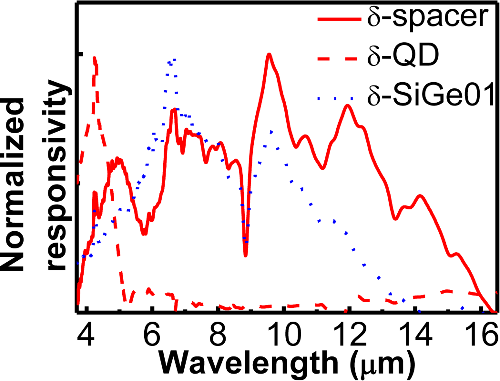
Spectral responses of MIS SiGe/Si quantum dot (well) infrared photodetectors are shown in Figure 26 [81]. The label “δ-spacer” and “δ-QD” indicated the MIS SiGe/Si QDIPs with boron doping in the Si spacers and SiGe QDs, respectively. The label “δ-SiGe01” indicated the MIS SiGe/Si quantum well infrared photodetector with boron doping in the Si0.9Ge0.1 quantum wells. For the spacer sample, the detection regions of 3.7–6 and 6–16 μm corresponded to the LH1-to-LH3 transition in SiGe/Si QDs, and intraband transitions in boron doping wells, respectively.
For the SiGe01 sample, since the depth of Si0.9Ge0.1 quantum wells would be very shallow unlike that of SiGe QDs (Ge composition of ∼0.5 [82]), the LH1-to-LH3 transition would not exist. Only the intraband transitions in the boron doping wells contributed to the detection spectrum. Due to the additional quantum confinement of the SiGe QW outside the boron doping well, the detection spectrum had a slight blue shift as compared with the spacer sample. For the QD sample, the excited holes via intraband transitions in the boron doping wells were subsequently blocked by the large valence band barrier of the SiGe/Si QDs. Hence, detection via intraband transitions in the boron doping wells was not observed, and only the narrow spectrum due to the LH1-to-LH3 transition in SiGe QDs was observed. Although the spectrum of the QD sample was narrower than that of the spacer sample, a lower dark current and larger detectivity was able to be achieved with such a structure [83].
6. Conclusions
Nowadays, integrated circuits are composed of MOSFETs. If the MIS structure can be utilized for photodetectors, the integration of detection devices and readout circuit will be much easier and less expensive to manufacture. The wide-bandgap semiconductor has been utilized in the MIS UV photodetectors, and the optimized UV-to-visible rejection ratio could be more than three orders of magnitude. Si-based and thin-film Ge MIS photodetectors are suitable for visible-to-near-IR photo-detection. With the MIS SiGe/Si QDIPs, a broadband infrared detection covering atmospheric transmission windows at 3–5.3 μm and 7.5–14 μm is possible.
References
- Monroy, E; Omnès, F; Calle, F. Wide-Bandgap Semiconductor Ultraviolet Photodetectors. Semicond. Sci. Technol 2003, 18, R33–R51. [Google Scholar]
- Park, JS; Lin, TL; Jones, EW; Castillo, HMD; Gunapala, SD. Long-Wavelength Stacked SiGe/Si Heterojunction Internal Photoemission Infrared Detectors Using Multiple SiGe/Si Layers. Appl. Phys. Lett 1994, 64, 2370–2372. [Google Scholar]
- Rogalski, A. Quantum Well Photoconductors in Infrared Detector Technology. J. Appl. Phys 2003, 93, 4355–4391. [Google Scholar]
- Kasper, E; Oehme, M. High Speed Germanium Detectors on Si. Phys. Stat. Sol. C 2008, 5, 3144–3149. [Google Scholar]
- Brennan, KF; Haralson, J; Parks, JW; Salem, A. Review of Reliability Issues of Metal-Semiconductor-Metal and Avalanche Photodiode Photonic Detectors. Microelectron. Reliab 1999, 39, 1873–1883. [Google Scholar]
- Lee, HC; Su, YK; Lin, JC; Cheng, YC; Wu, SL; Jhou, YD. AlInGaN Metal-Insulator-Semiconductor Photodetectors at UV-C 280 nm. Electrochem. Solid. St 2009, 12, H357–H360. [Google Scholar]
- Lo, SH; Buchanan, DA; Taur, Y; Wang, W. Quantum-Mechanical Modeling of Electron Tunneling Current from the Inversion Layer of Ultra-Thin-Oxide MOSFET’s. IEEE. Electron. Device. Lett 1997, 18, 209–211. [Google Scholar]
- Lee, WC; Hu, C. Modeling CMOS Tunneling Currents Through Ultrathin Gate Oxide Due to Conduction and Valence Band Electron and Hole Tunneling. IEEE. Trans. Electron. Devices 2001, 48, 1366–1373. [Google Scholar]
- Liu, CW; Liu, WT; Lee, MH; Kuo, WS; Hsu, BC. A Novel Photodetector Using MOS Tunneling Structures. IEEE. Electron. Device. Lett 2000, 21, 307–309. [Google Scholar]
- Lin, CH; Hsu, BC; Lee, MH; Liu, CW. A Comprehensive Study of Inversion Current in MOS Tunneling Diodes. IEEE. Trans. Electron. Devices 2001, 48, 2125–2130. [Google Scholar]
- Sze, SM; Ng, KK. Physics of Semiconductor Devices, 3rd ed; Wiley: Hoboken, NJ, USA, 2007; p. 682. [Google Scholar]
- Monroy, E; Calle, F; Pau, JL; Muñoz, E; Omnès, F; Beaumont, B; Gibart, P. Application and Performance of GaN Based UV Detectors. Phys. Stat. Sol. A 2001, 185, 91–97. [Google Scholar]
- Sze, SM; Ng, KK. Physics of Semiconductor Devices, 3rd ed; Wiley: Hoboken, NJ, USA, 2007; p. 678. [Google Scholar]
- Liu, CY; Chen, BY; Tseng, TY. Deep Depletion Phenomenon of SrTiO3 Gate Dielectric Capacitor. J. Appl. Phys 2004, 95, 5602–5607. [Google Scholar]
- Liu, J; Michel, J; Giziewicz, W; Pan, D; Wada, K; Cannon, DD; Jongthammanurak, S; Danielson, DT; Kimerling, LC. High-Performance, Tensile-Strained Ge p-i-n Photodetectors on a Si Platform. Appl Phys Lett 2005, 87, 103501:1–103501:3. [Google Scholar]
- Monroy, E; Calle, F; Pau, JL; Muñoz, E; Omnès, F. Low-Noise Metal-Insulator-Semiconductor UV Photodiodes Based on GaN. Electron. Lett 2000, 36, 2096–2098. [Google Scholar]
- Basak, D; Amin, G; Mallik, B; Paul, GK; Sen, SK. Photoconductive UV Detectors on Sol-Gel-Synthesized ZnO Films. J. Cryst. Growth 2003, 256, 73–77. [Google Scholar]
- Muñoz, E; Monroy, E; Pau, JL; Calle, F; Omnès, F; Gibart, P, III. Nitrides and UV Detection. J. Phys. Condens. Matter 2001, 13, 7115–7137. [Google Scholar]
- Chiou, YZ; Su, YK; Chang, SJ; Gong, J; Chang, CS; Liu, SH. The Properties of Photo Chemical-Vapor Deposition SiO2 and its Application in GaN Metal-Insulator Semiconductor Ultraviolet Photodetectors. J. Electron. Mater 2002, 32, 395–399. [Google Scholar]
- Lin, CH; Yu, CY; Peng, CY; Ho, WS; Liu, CW. Broadband SiGe/Si Quantum Dot Infrared Photodetectors. J Appl Phys 2007, 101, 033117:1–033117:4. [Google Scholar]
- Hwang, JD; Yang, GH; Yang, YY; Yao, PC. Nitride-Based UV Metal-Insulator-Semiconductor Photodetector with Liquid-Phase-Deposition Oxide. Jpn. J. Appl. Phys 2005, 44, 7913–7915. [Google Scholar]
- Walker, D; Kumar, V; Mi, K; Sandvik, P; Kung, P; Zhang, XH; Razeghi, M. Solar-Blind AlGaN Photodiodes with Very Low Cutoff Wavelength. Appl. Phys. Lett 2000, 76, 403–405. [Google Scholar]
- Chang, PC; Chen, CH; Chang, SJ; Su, YK; Yu, CL; Huang, BR; Chen, PC. High UV/visible Rejection Contrast AlGaN/GaN MIS Photodetectors. Thin Solid Films 2006, 498, 133–136. [Google Scholar]
- Walker, D; Saxler, A; Kung, P; Zhang, X; Hamilton, M; Diaz, J; Razeghi, M. Visible Blind GaN p-i-n Photodiodes. Appl. Phys. Lett 1998, 72, 3303–3305. [Google Scholar]
- Zhang, Y; Shen, SC; Kim, HJ; Choi, S; Ryou, JH; Dupuis, RD; Narayan, B. Low-Noise GaN Ultraviolet p-i-n Photodiodes on GaN Substrates. Appl Phys Lett 2009, 94, 221109:1–221109:3. [Google Scholar]
- Carrano, JC; Grudowski, PA; Eiting, CJ; Dupuis, RD; Campbell, JC. Very Low Dark Current Metal-Semiconductor-Metal Ultraviolet Photodetectors Fabricated on Single-Crystal GaN Epitaxial Layers. Appl. Phys. Lett 1997, 70, 1992–1994. [Google Scholar]
- Wang, CK; Chang, SJ; Su, YK; Chiou, YZ; Chen, SC; Chang, CS; Lin, TK; Liu, HL; Tang, JJ. GaN MSM UV Photodetectors with Titanium Tungsten Transparent Electrodes. IEEE. Trans. Electron. Devices 2006, 53, 38–42. [Google Scholar]
- Yang, W; Nohova, T; Krishnankutty, S; Torreano, R; McPherson, S; Marsh, H. Back-Illuminated GaN/AlGaN Heterojunction Photodiodes with High Quantum Efficiency and Low Noise. Appl. Phys. Lett 1998, 73, 1086–1088. [Google Scholar]
- Ozbay, E; Biyikli, N; Kimukin, I; Kartaloglu, T; Tut, T; Aytür, O. High-Performance Solar-Blind Photodetectors Based on AlxGa1-xN Heterostructures. IEEE. J. Sel. Top. Quantum Electron 2004, 10, 742–751. [Google Scholar]
- Razeghi, M; Rogalski, A. Semiconductor Ultraviolet Detectors. J. Appl. Phys 1996, 79, 7433–7473. [Google Scholar]
- Liu, CH; Chang, CS; Chang, SJ; Su, YK; Chiou, YZ; Liu, SH; Huang, BR. The Characteristics of Photo-CVD SiO2 and Its Application on SiC MIS UV Photodetectors. Mater. Sci. Eng. B 2003, 100, 142–146. [Google Scholar]
- Chen, X; Zhu, H; Cai, J; Wu, Z. High-Performance 4H-SiC-Based Ultraviolet p-i-n Photodetector. J Appl Phys 2007, 102, 024505:1–024505:4. [Google Scholar]
- Morkoc, H; Strite, S; Gao, GB; Lin, ME; Sverdlov, B; Burns, M. Large-Band-Gap SiC, III–V Nitride, and II–VI ZnSe-Based Semiconductor Device Technologies. J. Appl. Phys 1994, 76, 1363–1398. [Google Scholar]
- Lin, TK; Chang, SJ; Chiou, YZ; Wang, CK; Chang, SP; Lam, KT; Sun, YS; Huang, BR. Homoepitaxial ZnSe MIS Photodetectors with SiO2 and BST Insulator Layers. Solid. State. Electron 2006, 50, 750–753. [Google Scholar]
- Young, SJ; Ji, LW; Chang, SJ; Liang, SH; Lam, KT; Fang, TH; Chen, KJ; Du, XL; Xue, QK. ZnO-Based MIS Photodetectors. Sens. Actuat. A. Phys 2008, 141, 225–229. [Google Scholar]
- Tsukazaki, A; Ohtomo, A; Onuma, T; Ohtani, M; Makino, T; Sumiya, M; Ohtani, K; Chichibu, SF; Fuke, S; Segawa, Y; Ohno, H; Koinuma, H; Kawasaki, M. Repeated Temperature Modulation Epitaxy for p-Type Doping and Light-Emitting Diode Based on ZnO. Nature Mater 2005, 4, 42–46. [Google Scholar]
- Zhu, H; Shan, CX; Wang, LK; Zheng, J; Zhang, JY; Yao, B; Shen, DZ. Metal-Oxide-Semiconductor-Structured MgZnO Ultraviolet Photodetector with High Internal Gain. J. Phys. Chem. C 2010, 114, 7169–7172. [Google Scholar]
- Yang, W; Vispute, RD; Choopun, S; Sharma, RP; Venkatesan, T; Shen, H. Ultraviolet Photoconductive Detector Based on Epitaxial Mg0.34Zn0.66O Thin Films. Appl. Phys. Lett 2001, 78, 2787–2789. [Google Scholar]
- Ju, ZG; Shan, CX; Jiang, DY; Zhang, JY; Yao, B; Zhao, DX; Shen, DZ; Fan, XW. MgxZn1-xO-Based Photodetectors Covering the Whole Solar-Blind Spectrum Range. Appl Phys Lett 2008, 93, 173505:1–173505:3. [Google Scholar]
- Ho, WS; Lin, CH; Cheng, TH; Hsu, WW; Chen, YY; Kuo, PS; Liu, CW. Narrow-Band Metal-Oxide-Semiconductor Photodetector. Appl Phys Lett 2009, 94, 061114:1–061114:3. [Google Scholar]
- Hansen, TE. Silicon UV-Photodiodes Using Natural Inversion Layers. Phys. Scr 1978, 18, 471–475. [Google Scholar]
- Colace, L; Assanto, G; Fulgoni, D; Nash, L. Near-Infrared p-i-n Ge-on-Si Photodiodes for Silicon Integrated Receivers. J. Lightwave. Technol 2008, 26, 2954–2959. [Google Scholar]
- Sher, A; Tsuo, YH; Moriarty, JA; Miller, WE; Crouch, RK. Si and GaAs Photocapacitive MIS Infrared Detectors. J. Appl. Phys 1980, 51, 2137–2148. [Google Scholar]
- Malik, A; Grimalsky, V. Conception of the Optical Sensors Based on Transient Processed in MIS Structures. Sens. Actuat. A. Phys 2004, 110, 310–317. [Google Scholar]
- Malik, A; Grimalsky, V; Jacome, AT; Durini, D. Theoretical Modeling and Experimental Investigation of MIS Radiation Sensor with Giant Internal Signal Amplification. Sens. Actuat. A. Phys 2004, 114, 319–326. [Google Scholar]
- Thaniyavarn, S; Gustafson, TK. Metal/Tunnel-Barrier/Semiconductor/Tunnel-Barrier/Metal Fast Photodetector. Appl. Phys. Lett 1982, 40, 255–257. [Google Scholar]
- Fernandes, M; Vygranenko, Y; Schwarz, R; Vieira, M. ITO/SiOx/Si Optical Sensor with Internal Gain. Sens. Actuat. A. Phys 2001, 92, 152–155. [Google Scholar]
- Hsu, BC; Chang, ST; Shie, CR; Lai, CC; Chen, PS; Liu, CW. High Efficient 820 nm MOS Ge Quantum Dot Photodetectors for Short-Reach Integrated Optical Receivers with 1,300 and 1,550 nm Sensitivity. IEDM Tech Dig 2002, 91–94. [Google Scholar]
- Cheng, JY; Lu, HT; Hwu, JG. Metal-Oxide-Semiconductor Tunneling Photodiodes with Enhanced Deep Depletion at Edge by High-k Material. Appl Phys Lett 2010, 96, 233506:1–233506:3. [Google Scholar]
- Hsu, BC; Liu, CW; Liu, WT; Lin, CH. A PMOS Tunneling Photodetector. IEEE. Trans. Electron. Devices 2001, 48, 1747–1749. [Google Scholar]
- Hashimoto, H; Yamada, R; Hirokane, T; Arima, K; Uchikoshi, J; Morita, M. Photodetective Characteristics of Metal-Oxide-Semiconductor Tunneling Structure with Aluminum Grid Gate. Jpn. J. Appl. Phys 2007, 46, 2467–2470. [Google Scholar]
- Seto, M; Rochefort, C; Jager, SD; Hendriks, RFM; ’t Hooft, GW; Mark, MBVD. Low-Leakage-Current Metal-Insulator-Semiconductor-Insulator-Metal Photodetector on Silicon with a SiO2 Barrier-Enhancement Layer. Appl. Phys. Lett 1999, 75, 1976–1978. [Google Scholar]
- Hsu, BC; Chang, ST; Chen, TC; Kuo, PS; Chen, PS; Pei, Z; Liu, CW. A High Efficient 820 nm MOS Ge Quantum Dot Photodetector. IEEE. Electron. Device. Lett 2003, 24, 318–320. [Google Scholar]
- Binari, SC; Miller, WE; Sher, A; Tsuo, YH. Ge Photocapacitive MIS Infrared Detectors. J. Appl. Phys 1979, 50, 7883–7886. [Google Scholar]
- Cheng, TH; Liao, MH; Yeh, L; Lee, TL; Liang, MS. Digital Communication Using Ge Metal-Insulator-Semiconductor Light-Emitting Diodes and Photodetectors. J Appl Phys 2008, 103, 016103:1–016103:3. [Google Scholar]
- Kuo, PS; Fu, YC; Chang, CC; Lee, CH; Liu, CW. Dark Current Reduction of Ge MOS Photodetectors by High Work Function Electrodes. Electron. Lett 2007, 43, 1113–1114. [Google Scholar]
- Morse, M; Dosunmu, O; Sarid, G; Chetrit, Y. Performance of Ge-on-Si p-i-n Photodetectors for Standard Receiver Modules. IEEE. Photon. Technol. Lett 2006, 18, 2442–2444. [Google Scholar]
- Zang, H; Lee, SJ; Loh, WY; Wang, J; Yu, MB; Lo, GQ; Kwong, DL; Cho, BJ. Application of Dopant Segregation to Metal-Germanium-Metal Photodetectors and Its Dark Current Suppression Mechanism. Appl Phys Lett 2008, 92, 051110:1–051110:3. [Google Scholar]
- Yu, CY; Lee, CY; Lin, CH; Liu, CW. Low-Temperature Fabrication and Characterization of Ge-on-Insulator Structures. Appl Phys Lett 2006, 89, 101913:1–101913:3. [Google Scholar]
- Nishimura, T; Kita, K; Toriumi, A. Evidence for Strong Fermi-Level Pinning Due to Metal-Induced Gap States at Metal/Germanium Interface. Appl Phys Lett 2007, 91, 123123:1–123123:3. [Google Scholar]
- Lieten, RR; Degroote, S; Kuijk, M; Borghs, G. Ohmic Contact Formation on n-Type Ge. Appl Phys Lett 2008, 92, 022106:1–022106:3. [Google Scholar]
- Lin, CH; Chiang, YT; Hsu, CC; Lee, CH; Huang, CF; Lai, CH; Cheng, TH; Liu, CW. Ge-on-Glass Detectors. Appl Phys Lett 2007, 91, 041105:1–041105:3. [Google Scholar]
- Ho, WS; Dai, YH; Deng, Y; Lin, CH; Chen, YY; Lee, CH; Liu, CW. Flexible Ge-on-Polyimide Detectors. Appl Phys Lett 2009, 94, 261107:1–261107:3. [Google Scholar]
- Heyns, M; Meuris, M; Caymax, M. Ge and III/V as Enabling Materials for Future CMOS Technologies. ECS Trans 2006, 3, 511–518. [Google Scholar]
- Rogalski, A. Infrared Detectors: Status and Trends. Prog. Quantum. Electron 2003, 27, 59–210. [Google Scholar]
- Deng, SY; Lee, JYM; Lai, JT; Chih, YD; Sun, TP; Hong, HM. Front-Illuminated Long Wavelength Multiple Quantum-Well Infrared Photodetectors with Backside Gratings. J. Appl. Phys 1995, 78, 6822–6825. [Google Scholar]
- Finkman, E; Maimon, S; Immer, V; Bahir, G; Schacham, SE; Fossard, F; Julien, FH; Brault, J; Gendry, M. Polarized Front-Illumination Response in Intraband Quantum Dot Infrared Photodetectors at 77 K. Phys Rev B 2001, 63, 045323:1–045323:7. [Google Scholar]
- Rogalski, A. HgCdTe Infrared Detector Material: History, Status and Outlook. Rep. Prog. Phys 2005, 68, 2267–2336. [Google Scholar]
- Singh, R; Gupta, AK; Chhabra, KC. Surface Passivation of Mercury-Cadmium-Telluride Infrared Detectors. Def. Sci. J 1991, 41, 205–239. [Google Scholar]
- Kinch, MA. MIS Devices in HgCdTe. In Properties of Narrow Gap Cadmium-Based Compounds (EMIS Datareviews Series No 10); Capper, P, Ed.; INSPEC, IEE: London, UK, 1994; pp. 359–363. [Google Scholar]
- Lee, TS; Choi, KK; Jeoung, YT; Kim, HK; Kim, JM; Kim, YH; Chang, JM; Song, WS; Kim, SU; Park, MJ; Lee, SD. Surface Passivation of HgCdTe by CdZnTe and Its Characteristics. J. Electron. Mater 1997, 26, 552–555. [Google Scholar]
- Jung, YC; An, SY; Suh, SH; Choi, DK; Kim, JS. Ammonium Sulfide Treatment of HgCdTe Substrate and Its Effects on Electrical Properties of ZnS/HgCdTe Heterostructure. Thin Solid Films 2005, 483, 407–410. [Google Scholar]
- Damnjanoviè, V; Ponomarenko, VP; Elazar, JM. Photo-Electric Characteristics of HgCdTe Tunnel MIS Photo-Detectors. Semicond Sci Technol 2009, 24, 025003:1–025003:6. [Google Scholar]
- Karunasiri, RPG; Park, JS; Wang, KL. Si1-xGex/Si Multiple Quantum Well Infrared Detector. Appl. Phys. Lett 1991, 59, 2588–2590. [Google Scholar]
- Kruck, P; Helm, M; Fromherz, T; Bauer, G; Nützel, JF; Abstreiter, G. Medium-Wavelength, Normal-Incidence, p-Type Si/SiGe Quantum Well Infrared Photodetector with Background Limited Performance up to 85 K. Appl. Phys. Lett 1996, 69, 3372–3374. [Google Scholar]
- Tong, S; Liu, F; Khitun, A; Wang, KL; Liu, JL. Tunable Normal Incidence Ge Quantum Dot Midinfrared Detectors. J. Appl. Phys 2004, 96, 773–776. [Google Scholar]
- Hsu, BC; Lin, CH; Kuo, PS; Chang, ST; Chen, PS; Liu, CW; Lu, JH; Kuan, CH. Novel MIS Ge-Si Quantum-Dot Infrared Photodetectors. IEEE. Electron. Device. Lett 2004, 25, 544–546. [Google Scholar]
- Liu, JL; Wu, WG; Balandin, A; Jin, GL; Wang, KL. Intersubband Absorption in Boron-Doped Multiple Ge Quantum Dots. Appl. Phys. Lett 1992, 74, 185–187. [Google Scholar]
- Kuo, PS; Lin, CH; Peng, CY; Fu, YC; Liu, CW. Transport Mechanism of SiGe Dot MOS Tunneling Diodes. IEEE. Electron. Device. Lett 2007, 28, 596–598. [Google Scholar]
- Lin, CH; Yu, CY; Kuo, PS; Chang, CC; Guo, TH; Liu, CW. Doped MOS Ge/Si Quantum Dot/Well Infrared Photodetector. Thin Solid Films 2006, 508, 389–392. [Google Scholar]
- Lin, CH; Yu, CY; Chang, CC; Lee, CH; Yang, YJ; Ho, WS; Chen, YY; Liao, MH; Cho, CT; Peng, CY; Liu, CW. SiGe/Si Quantum-Dot Infrared Photodetectors with Doping. IEEE Trans. Nanotech 2008, 7, 558–564. [Google Scholar]
- Liao, MH; Lee, CH; Hung, TA; Liu, CW. The Intermixing and Strain Effects on Electroluminescence of SiGe Dots. J Appl Phys 2007, 102, 053520:1–053520:5. [Google Scholar]
- Lin, CH; Liu, CW. Metal-Oxide-Semiconductor SiGe/Si Quantum Dot Infrared Photodetectors with Delta Doping in Different Positions. Thin Solid Films 2010, 518, S237–S240. [Google Scholar]
Figure 1.
Gate tunneling current as a function of oxide thickness for various gate biases. In this example, the gate tunneling current is dominated by election tunneling from the conduction band of the vertical NMOS diode of an NMOSFET [7,8].
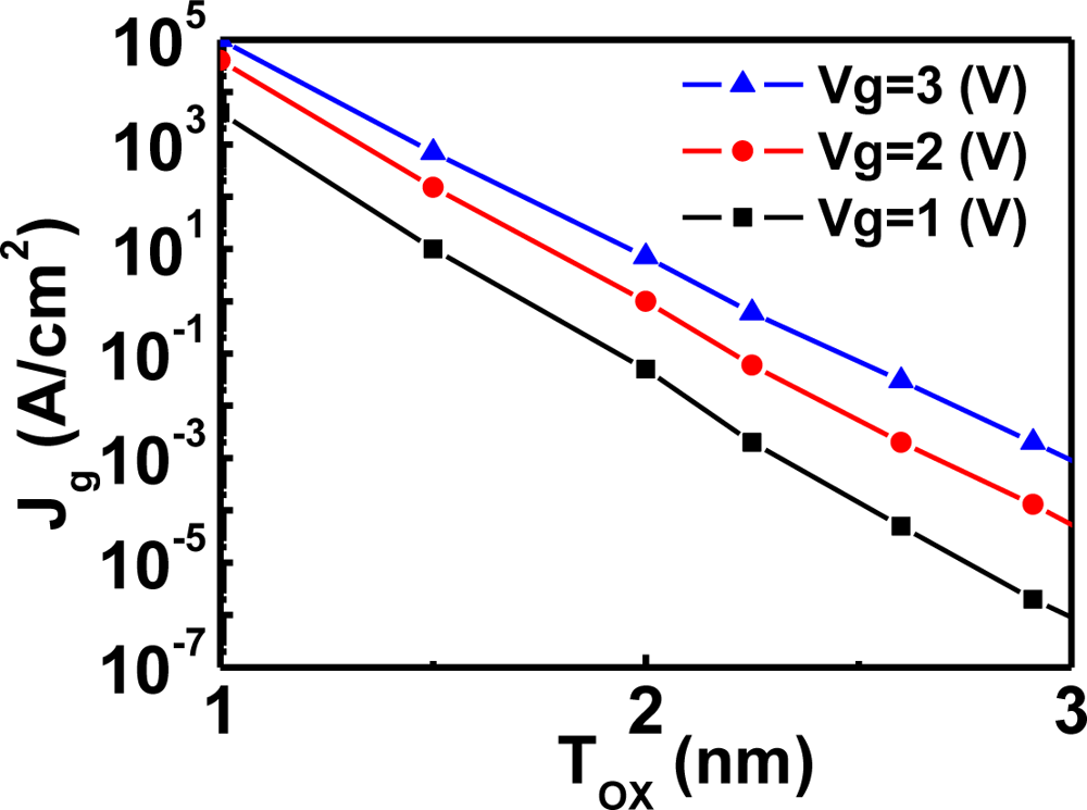
Figure 2.
(a) The oxide voltage as a function of the gate voltage for a 3-nm-oxide NMOS with an NMOSFET transistor structure [8] and a 2.3 nm oxide NMOS without a transistor structure [9]; (b) Gate tunneling current density as a function of the gate voltage for a 2.9 nm oxide NMOS with an NMOSFET transistor structure [8] and a 2.3 nm oxide NMOS without a transistor structure [9].
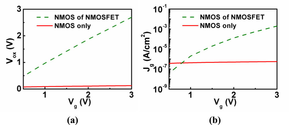
Figure 3.
The current mechanisms of an MIS diode (a) without light illumination; (b) with light illumination. A positive bias (inversion bias) is applied for this metal/insulator/p-type semiconductor example.
Figure 3.
The current mechanisms of an MIS diode (a) without light illumination; (b) with light illumination. A positive bias (inversion bias) is applied for this metal/insulator/p-type semiconductor example.

Figure 4.
The schematic structures of metal-insulator-semiconductor photodetectors. (a) Light irradiates into the semiconductor from the unshadowed region when the metal is not transparent; (b) Light irradiates into the semiconductor passing through the transparent conducting oxide (TCO) or thin semi-transparent metal film.

Figure 5.
Three different AlGaN/GaN structures: (a) MSM detector; (b) MIS detector without anti-reflection coating and (c) MIS detector with anti-reflection coating. The 50 nm thick SiO2 layer in (c) acts as both a passivation layer and anti-reflection coating. Reproduced from [23] with permission of Elsevier (2006).
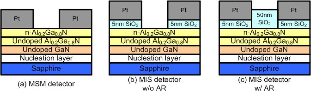
Figure 6.
Spectral responsivities of these three different photodetectors shown in Figure 5. The AlGaN/GaN MIS photodetector with AR coating has the highest UV-to-visible rejection ratio. Reproduced from [23] with permission of Elsevier (2006).
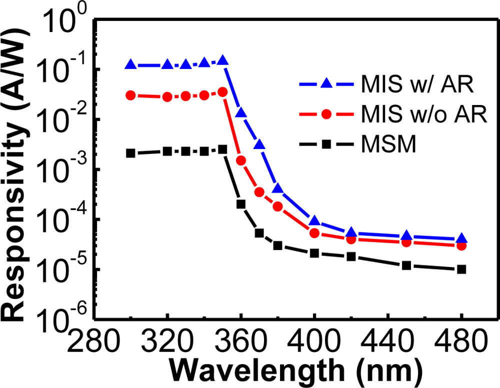
Figure 7.
Spectral responsivity of the ITO/SiO2/SiC MIS photodetector. The UV (310 nm)-to-visible (500 nm) rejection ratio was ∼80. Reproduced from [31] with permission of Elsevier (2003).
Figure 7.
Spectral responsivity of the ITO/SiO2/SiC MIS photodetector. The UV (310 nm)-to-visible (500 nm) rejection ratio was ∼80. Reproduced from [31] with permission of Elsevier (2003).

Figure 8.
Responsivity as a function of applied voltage for the Au/MgO/MgZnO MIS and Au/MgZnO MS photodetectors. The responsivity of the MIS detector increased exponentially, meanwhile the MS detector showed a linear behavior. Reproduced from [37] with permission of the American Chemical Society (2010).
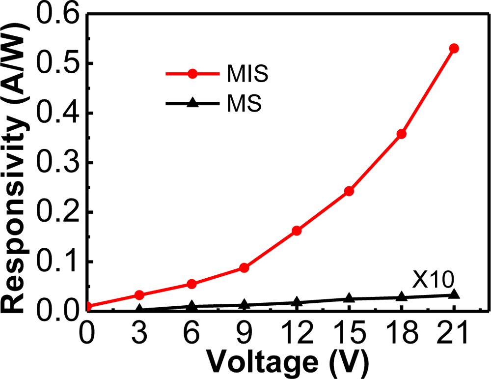
Figure 9.
The schematic mechanism of optical gain in the MIS photodetector. With the multiplication process, the external quantum efficiency of the MIS detector could achieve 200% at 21 V [37].
Figure 9.
The schematic mechanism of optical gain in the MIS photodetector. With the multiplication process, the external quantum efficiency of the MIS detector could achieve 200% at 21 V [37].
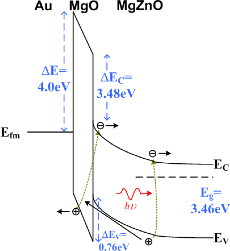
Figure 10.
The schematic structure of a metal-filter (such as Ag) Si MIS UV photodetector. Incident photons were firstly selected by the gate, and then the remaining photons might be absorbed by Si to form the photocurrent.
Figure 10.
The schematic structure of a metal-filter (such as Ag) Si MIS UV photodetector. Incident photons were firstly selected by the gate, and then the remaining photons might be absorbed by Si to form the photocurrent.
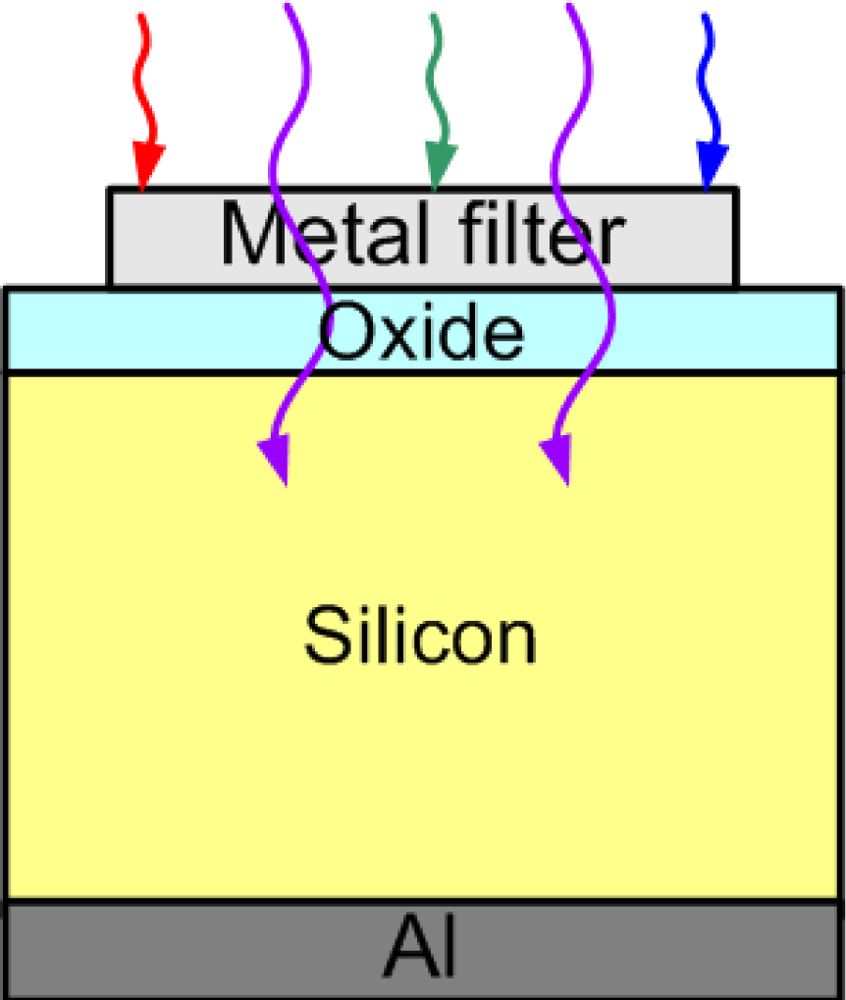
Figure 11.
Spectral responsivities of the Ag/SiO2/Si photodetectors with different thicknesses of Ag. The transmission of UV band at the ∼319 nm wavelength was due to the material property of Ag [40].
Figure 11.
Spectral responsivities of the Ag/SiO2/Si photodetectors with different thicknesses of Ag. The transmission of UV band at the ∼319 nm wavelength was due to the material property of Ag [40].

Figure 12.
Dark current and photocurrents of the (a) Al/SiO2/p-Si MIS (NMOS) diode; (b) Al/SiO2/n-Si MIS (PMOS) diode. The inversion biases were positive and negative voltages for NMOS and PMOS photodetectors, respectively [9,50].
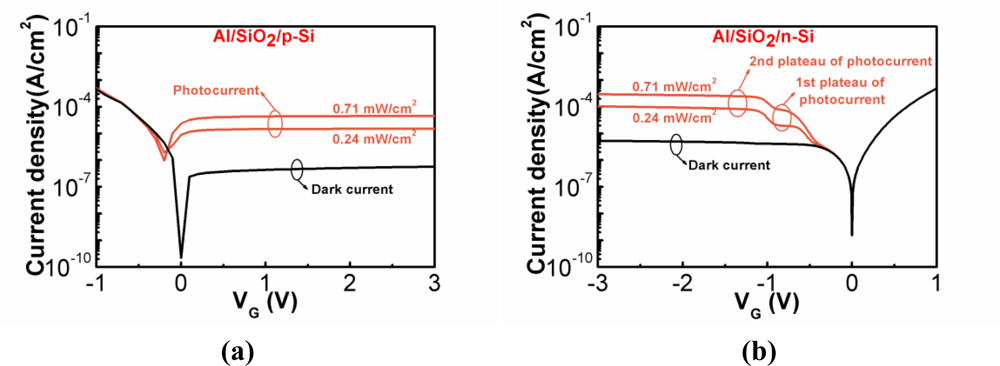
Figure 13.
The schematic diagram of an Al/SiO2/n-Si MIS (PMOS) diode. The photo-generated holes contributed to the first plateau of the photocurrent and the electron direct tunneling contributed to the second plateau [50].
Figure 13.
The schematic diagram of an Al/SiO2/n-Si MIS (PMOS) diode. The photo-generated holes contributed to the first plateau of the photocurrent and the electron direct tunneling contributed to the second plateau [50].
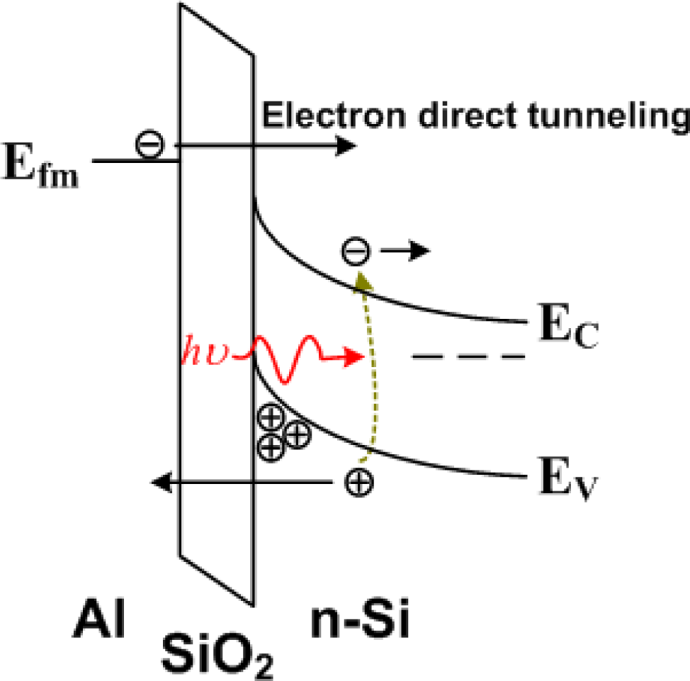
Figure 14.
The schematic structure of a metal-insulator-semiconductor-insulator-metal photodetector. Both the anode and cathode electrodes were on the thin-insulator side.
Figure 14.
The schematic structure of a metal-insulator-semiconductor-insulator-metal photodetector. Both the anode and cathode electrodes were on the thin-insulator side.

Figure 15.
The process flow of liquid phase deposition. The process can be operated at the temperature below 100 °C, and a thin (∼2 nm) SiO2 layer can be deposited on the Ge substrate [53].
Figure 15.
The process flow of liquid phase deposition. The process can be operated at the temperature below 100 °C, and a thin (∼2 nm) SiO2 layer can be deposited on the Ge substrate [53].

Figure 16.
Data communication system using a Ge MIS photodetector and a Ge MIS LED. The same MIS structure was used with different biases for different applications. The Ge MIS structure with an inversion bias acted as a detector, while it acted as an LED with an accumulation bias [55].
Figure 16.
Data communication system using a Ge MIS photodetector and a Ge MIS LED. The same MIS structure was used with different biases for different applications. The Ge MIS structure with an inversion bias acted as a detector, while it acted as an LED with an accumulation bias [55].
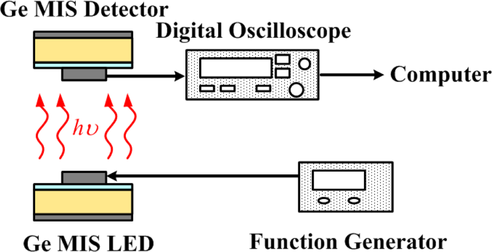
Figure 17.
Modulation results of the data communication using a Ge MIS photodetector and a Ge MIS LED with a frequency of (a) 300 Kbit/sec; (b) 15 Mbit/sec. A delay time of ∼19 ns was observed in (b). Reprinted from [55] with permission of the American Institute of Physics (Copyright 2008).
Figure 17.
Modulation results of the data communication using a Ge MIS photodetector and a Ge MIS LED with a frequency of (a) 300 Kbit/sec; (b) 15 Mbit/sec. A delay time of ∼19 ns was observed in (b). Reprinted from [55] with permission of the American Institute of Physics (Copyright 2008).
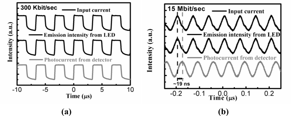
Figure 18.
The dark currents of Al/SiO2/n-Ge and Pt/SiO2/n-Ge photodetectors. The dark inversion current of the Pt gate device was smaller due to the suppression of electron tunneling from the metal to n-Ge [56].
Figure 18.
The dark currents of Al/SiO2/n-Ge and Pt/SiO2/n-Ge photodetectors. The dark inversion current of the Pt gate device was smaller due to the suppression of electron tunneling from the metal to n-Ge [56].

Figure 19.
The smart-cut process flow for demonstrating the GOI MIS photodetector. Thin films of 0.8–1.3 μm thick Ge were able to be transferred to the handle wafer.
Figure 19.
The smart-cut process flow for demonstrating the GOI MIS photodetector. Thin films of 0.8–1.3 μm thick Ge were able to be transferred to the handle wafer.
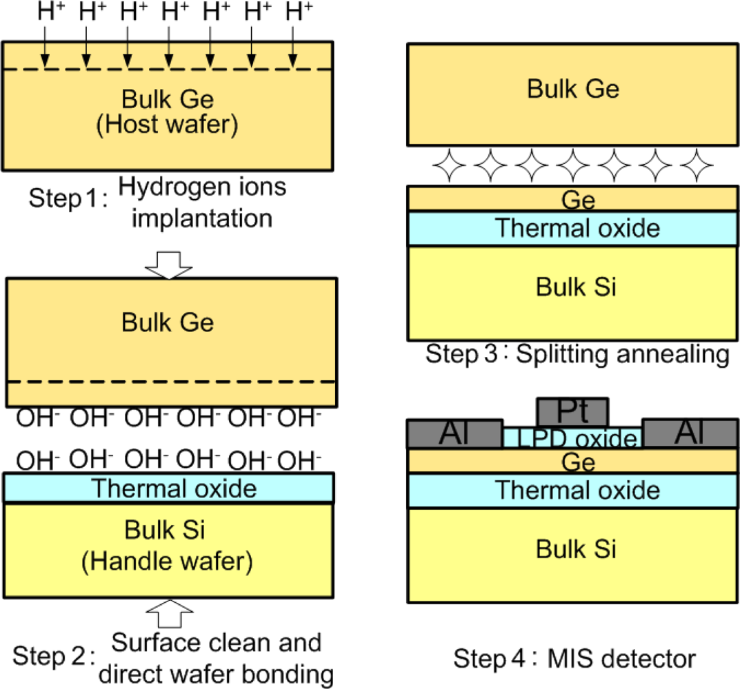
Figure 20.
The TEM photograph of the 0.8 μm thick-Ge GOI MIS photodetector. The low-temperature LPD SiO2 was formed on the thin-film Ge instead of the unstable GeO2.
Figure 20.
The TEM photograph of the 0.8 μm thick-Ge GOI MIS photodetector. The low-temperature LPD SiO2 was formed on the thin-film Ge instead of the unstable GeO2.
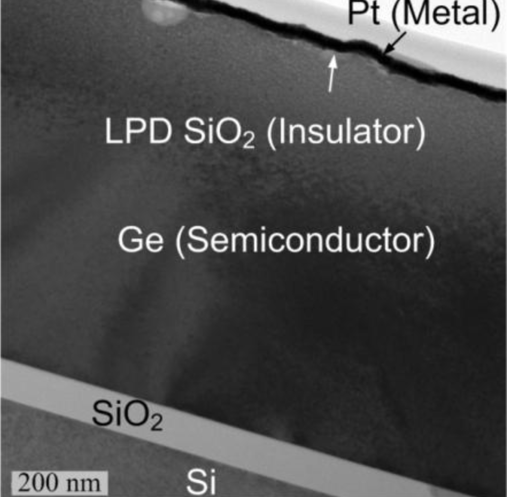
Figure 21.
Dark currents and photocurrents of the 1.3 μm thick-Ge GOI MIS and SB photodetectors. As compared with the SB detector, the MIS detector had a smaller dark current and a larger responsivity.
Figure 21.
Dark currents and photocurrents of the 1.3 μm thick-Ge GOI MIS and SB photodetectors. As compared with the SB detector, the MIS detector had a smaller dark current and a larger responsivity.

Figure 22.
The responsivities of: (a) GOG MIS photodetectors; (b) GOP MIS photodetectors. Reprinted from [62,63] with permission of the American Institute of Physics (Copyright 2007 & 2009).
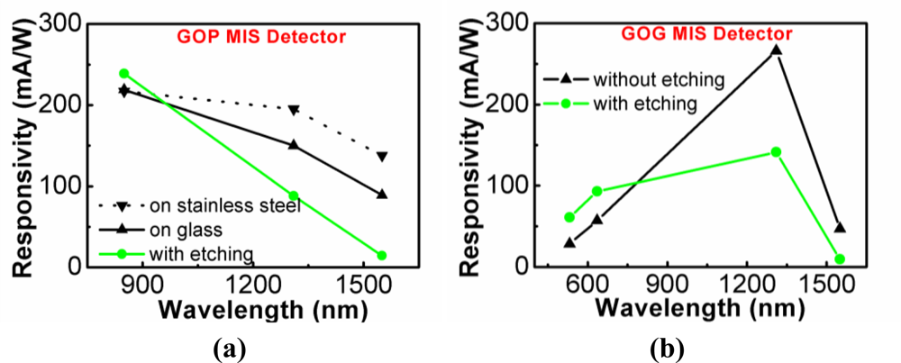
Figure 23.
The typical structure of the HgCdTe MIS photodetectors. A pulse of voltage was applied to induce a deep-depletion region in the HgCdTe semiconductor for separation of photo-generated carriers.
Figure 23.
The typical structure of the HgCdTe MIS photodetectors. A pulse of voltage was applied to induce a deep-depletion region in the HgCdTe semiconductor for separation of photo-generated carriers.
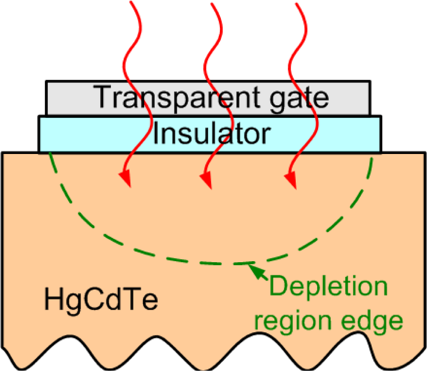
Figure 24.
The schematic structure of MIS SiGe/Si QDIPs. The low-temperature LPD SiO2 layer was adopted in order to avoid the strain relaxation and interdiffusion between Si and Ge.
Figure 24.
The schematic structure of MIS SiGe/Si QDIPs. The low-temperature LPD SiO2 layer was adopted in order to avoid the strain relaxation and interdiffusion between Si and Ge.
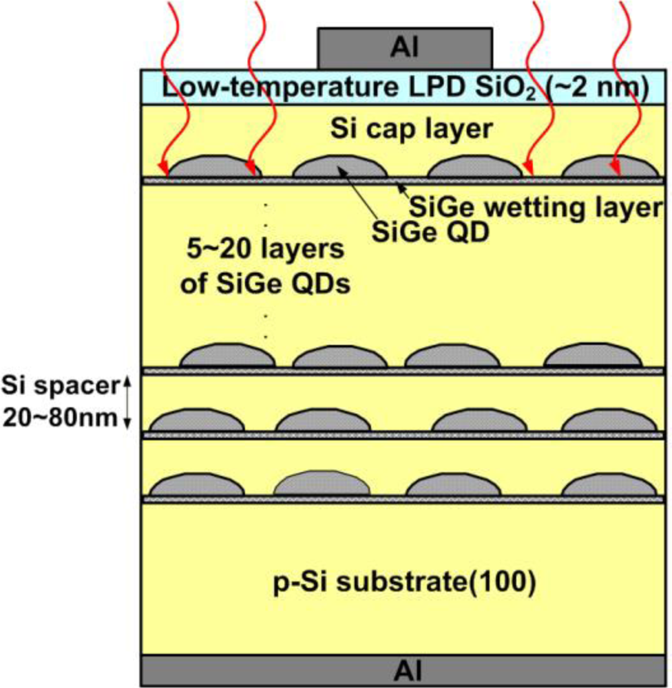
Figure 25.
Dark currents of five-period SiGe/Si QDIPs with and without an insulator layer between the metal and semiconductor. A QD sample with the insulator layer indeed can reduce the dark inversion current. Reproduced from [80] with permission of Elsevier (2006).
Figure 25.
Dark currents of five-period SiGe/Si QDIPs with and without an insulator layer between the metal and semiconductor. A QD sample with the insulator layer indeed can reduce the dark inversion current. Reproduced from [80] with permission of Elsevier (2006).
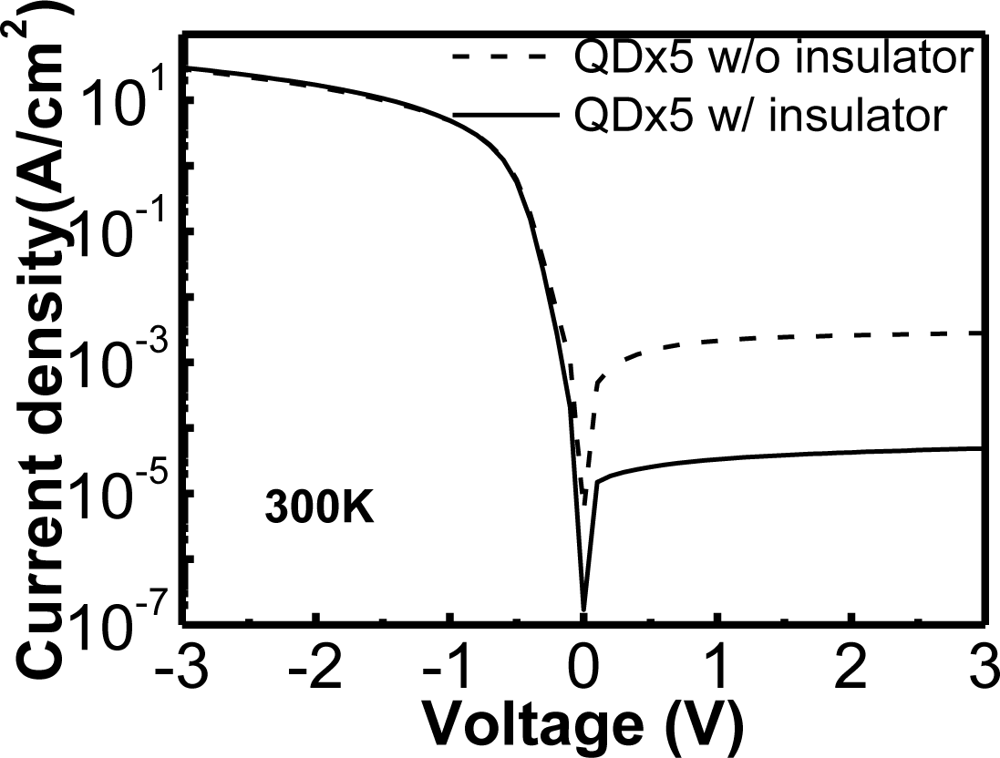
Figure 26.
Spectral responses of the MIS SiGe/Si quantum dot (well) infrared photodetectors at 15 K. For the spacer sample, the detection regions of 3.7–6 and 6–16 μm corresponded to the LH1-to-LH3 transition in QDs, and intraband transitions in the boron doping wells, respectively [83].
Figure 26.
Spectral responses of the MIS SiGe/Si quantum dot (well) infrared photodetectors at 15 K. For the spacer sample, the detection regions of 3.7–6 and 6–16 μm corresponded to the LH1-to-LH3 transition in QDs, and intraband transitions in the boron doping wells, respectively [83].

| Device | Jrev (Jinv) (A/cm2) | Responsivity (mA/W) | Detectivity (cmHz0.5W−1) | Rejection ratio | Ref. |
|---|---|---|---|---|---|
| MIS ITO/photo-SiO2/GaN | 5 × 10⁻⁷ @1 V | 110@338 nm@3 V | 2 × 10⁸@16 V | ∼200@3 V | [19] |
| MIS Al/LPD-SiO2/GaN | 7 × 10⁻⁷ @1 V | 112@366 nm@10 V | [21] | ||
| p-i-n GaN | 6 × 10⁻⁸@1 V | 150@363 nm@0 V | 106@0 V | [24] | |
| p-i-n GaN | 4 × 10⁻¹¹@10 V | 140@360 nm@20 V | 1.7 × 10¹⁴@20 V | 8×10³@20 V | [25] |
| MSM GaN | 4.5 × 10⁻⁶@10 V | 300@350 nm@6 V | ∼200@6 V | [26] | |
| MSM GaN | 10−6@1 V | 192@361 nm@3 V | 6.4 × 10⁹@3 V | ∼103@3 V | [27] |
| MIS AlGaN/GaN | ∼10−6 @1 V | 144@350 nm@5 V | 3,000@5 V | [23] | |
| p-i-n AlGaN/GaN | 6 × 10⁻¹⁰ @1 V | 200@355 nm@0 V | 104@0 V | [28] | |
| p-i-n AlGaN/GaN | 3 × 10⁻¹¹ @6 V | 65@267 nm@0 V | 4.9 × 10¹⁴@0 V | ∼104@0 V | [29] |
| MSM AlGaN/GaN | ∼10−6 @6 V | 2@264 nm@0 V | 8.9 × 10¹⁰@0 V | 2 × 10⁴@0 V | [29] |
| MSM AlGaN/GaN | ∼10−3 @1 V | 2@350 nm@5 V | 200@5 V | [23] | |
© 2010 by the authors; licensee MDPI, Basel, Switzerland. This article is an open access article distributed under the terms and conditions of the Creative Commons Attribution license (http://creativecommons.org/licenses/by/3.0/).
Share and Cite
MDPI and ACS Style
Lin, C.-H.; Liu, C.W. Metal-Insulator-Semiconductor Photodetectors. Sensors 2010, 10, 8797-8826. https://doi.org/10.3390/s101008797
AMA Style
Lin C-H, Liu CW. Metal-Insulator-Semiconductor Photodetectors. Sensors. 2010; 10(10):8797-8826. https://doi.org/10.3390/s101008797
Chicago/Turabian StyleLin, Chu-Hsuan, and Chee Wee Liu. 2010. "Metal-Insulator-Semiconductor Photodetectors" Sensors 10, no. 10: 8797-8826. https://doi.org/10.3390/s101008797