Article

Supramolecular Layer-by-Layer Assembly of 3D Multicomponent Nanostructures via Multivalent Molecular Recognition

1
Molecular Nanofabrication Group, MESA+ Institute for Nanotechnology, University of Twente, P.O. Box 217, 7500 AE, Enschede, The Netherlands
2
Materials Science and Technology of Polymers, MESA+ Institute for Nanotechnology, University of Twente, P.O. Box 217, 7500 AE, Enschede, The Netherlands
*
Author to whom correspondence should be addressed.
Int. J. Mol. Sci. 2008, 9(4), 486-497; https://doi.org/10.3390/ijms9040486
Submission received: 8 February 2008 / Revised: 26 March 2008 / Accepted: 31 March 2008 / Published: 4 April 2008

Abstract

:
The supramolecular layer-by-layer assembly of 3D multicomponent nanostructures of nanoparticles is demonstrated. Nanoimprint lithography (NIL) was used as the patterning tool for making patterned β-cyclodextrin (CD) self-assembled monolayers (SAMs) and for the confinement of nanoparticles on the substrate. A densely packed and multilayered nanoparticle structure was created by alternating assembly steps of complementary guest- (Fc-SiO2, 60 nm) and host-functionalized (CD-Au, 3 nm) nanoparticles. The effects induced by the order of the nanoparticle assembly steps, going from large to small and from small to large nanoparticles by using Fc-SiO2, CD-Au, and CD-SiO2 (350 nm) nanoparticles, were compared. AFM height profiles revealed that the specific supramolecular assembly of nanoparticles was self-limited, i.e. one nanoparticle layer per assembly step, allowing the control over the thickness of the supramolecular hybrid nanostructure by choosing the size of the nanoparticles, irrespective of the core material of the nanoparticles. The roughness of structure, observed by AFM imaging of the top layer, was directly influenced by the size and packing of the underlying nanoparticle layers.

1. Introduction

The assembly of three-dimensional composite nanomaterials has attracted a lot of interest owing to their fascinating optical, electrical and chemical properties that are different from the respective bulk materials [14], and to the need for the development of functional and miniaturized particle-based devices. The control over the lateral dimensions, thickness and composition of the nanomaterials at the nanometer range is particularly crucial. Several assembly techniques have been studied in order to direct nanoparticles into single or multicomponent 3D nanomaterials on surfaces. These are grouped in physical assembly techniques, e.g. convective assembly [5,6], spin coating [7], and spraying [8], and chemical assembly ones, e.g. electrostatic interactions [913], thiol-based self-assembly [14,15], supramolecular chemistry [1618], and coordination chemistry [19]. These techniques are commonly combined with layer-by-layer (LbL) assembly schemes [20], which involve the alternating adsorption of species with complementary interacting groups to construct multilayered and/or multicomponent nanomaterials.
By combining assembly techniques with top-down lithography, nanostructures with accurate spatial confinement can be fabricated [21]. One of the most commonly used techniques is microcontact printing [22]. Hammond et al. demonstrated the selective fabrication of multilayered and multicomponent nanoparticle arrays on microcontact-printed surfaces via electrostatic LbL assembly, with the underlying polyelectrolyte layers as an adhesive [23,24]. Tsukruk et al. reported freely suspended polymeric monolayers with a metal nanoparticle intralayer fabricated by spin-assisted LbL assembly, which thus resulted in a nanocomposite membrane suitable for application in sensors [25]. Recently, our group reported the use of nanoimprint lithography (NIL) as a tool to pattern self-assembled monolayers (SAMs) and nanoparticles on silicon substrates, which allows patterning of 3D features [26]. An aminoalkylsilane monolayer was first formed on the uncovered regions of the NIL-patterned substrates, which resulted in selective attachment of carboxylate-functionalized polystyrene and silica nanoparticles onto the patterned surfaces by electrostatic interactions.
Supramolecular host-guest interactions, owing to their highly tunable binding strength and reversibility [27,28], have been exploited for the assembly of receptor-functionalized molecules and nanoparticles onto interfaces with molecular recognition abilities. Our group has introduced the concept of ‘molecular printboards’ [29], which are β-cyclodextrin (CD) SAMs on gold or silicon oxide substrates that possess supramolecular host properties [30,31]. By using adamantyl- or ferrocenyl-functionalized dendrimers as a noncovalent supramolecular glue [32,33], CD-functionalized gold (CD-Au) and silica (CD-SiO2) nanoparticles were assembled onto CD SAMs [16,34]. Recently, we also reported ferrocenyl-functionalized silica (Fc-SiO2) nanoparticles, which can be directly adsorbed onto molecular printboards via host-guest recognition [18]. All of these host- or guest- functionalized nanoparticle layers bind strongly at the interface owing to the formation of multivalent host-guest interactions [29].
Here, we describe the attachment of alternating host- and guest-functionalized nanoparticles onto NIL-patterned molecular printboards, using nanoparticles of different sizes and core materials. The aim is to further extend the supramolecular LbL methodology to the buildup of multicomponent hybrid (organic-metallic-inorganic) nanoobjects by using nanoparticles functionalized with supramolecular interaction motifs that allow specific adsorption onto surfaces with complementary recognition properties. Three types of nanoparticles of different sizes were used, i.e. CD-functionalized Au (CD-Au, d ∼3 nm), ferrocenyl-functionalized silica nanoparticles (Fc-SiO2, d ∼60 nm), and CD-functionalized silica nanoparticles (CD-SiO2, d ∼350 nm). Guest- and host-functionalized nanoparticles were alternatingly assembled in a LbL scheme. The effects of the order of the nanoparticle assembly steps, from large to small and from small to large nanoparticles, were compared.

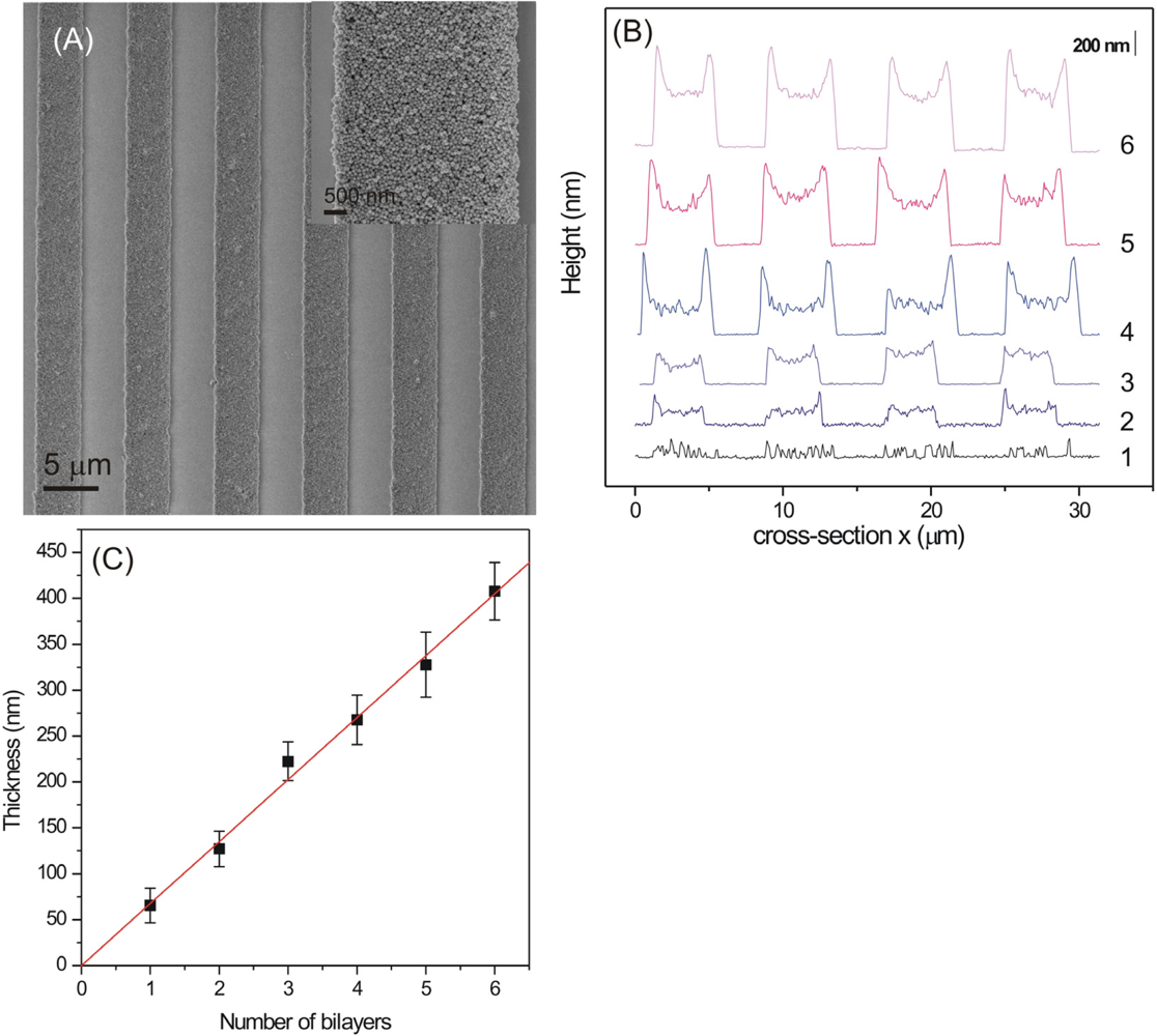
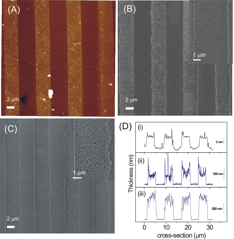
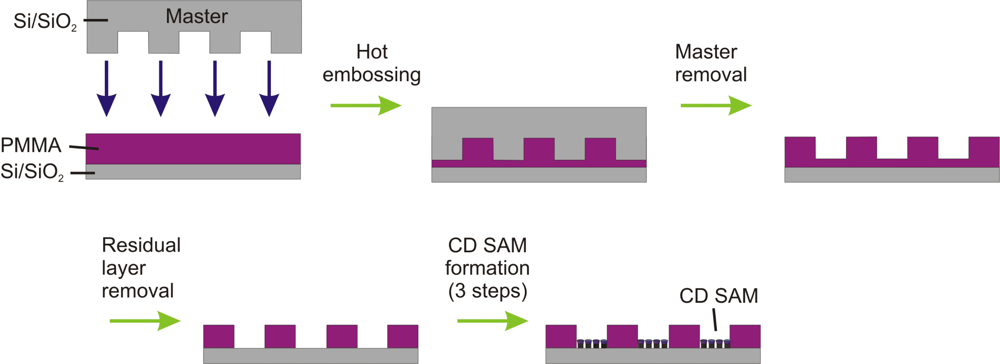
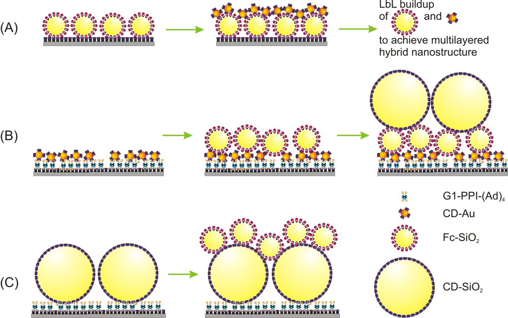
2. Results and Discussion

The aim of this study was to chemically direct the assembly of different types of functionalized nanoparticles onto a patterned substrate, such that a submicron 3D architecture constructed from different materials is obtained. Scheme 1 illustrates the fabrication process of a NIL-patterned CD SAM. NIL was used as the patterning technique in order to allow the directed assembly onto the patterned CD SAM and to provide physical confinement for the assembly of nanoparticles onto the substrate. To fabricate a patterned substrate, a piranha-cleaned silicon substrate spin-coated with a 500 nm thick layer of PMMA was pressed against a hard stamp at high temperature to form patterned substrates with 3.5 μm wide polymer lines. The residual layer in the imprinted areas was removed sonicating the substrate in acetone for 30 s. The CD SAMs were subsequently formed on the native SiO2 areas according to a previously described procedure [17].
Scheme 2 shows the preparation of multilayered and multicomponent nanostructures constructed from the LbL assembly of host- and guest-functionalized nanoparticles at NIL-patterned molecular printboards. Combinations of organic molecules and metallic and inorganic nanoparticles were used for the buildup of multilayered and multicomponent nanoparticle arrays, i.e., generation 1 adamantyl-functionalized poly(propyleneimine) dendrimers (G1-PPI-(Ad)4), ferrocenyl-functionalized silica nanoparticles (Fc-SiO2, d ∼60 nm), CD-functionalized gold (CD-Au, d ∼3 nm) and silica nanoparticles (CD-SiO2, d ∼350 nm).
In order to demonstrate the suitability of supramolecular LbL assembly for the control over the thickness of a 3D nanostructure, a supramolecular LbL assembly of alternating host-and guest-functionalized nanoparticles on NIL-patterned CD SAMs was performed. The complementary Fc-SiO2 (60 nm) and CD-Au (3 nm) were used as the specific guest-and host-functionalized building blocks to achieve an inorganic-metallic hybrid nanostructure at the molecular printboard with controllable height.
Figure 1A shows a typical image of the nanoparticle lines formed by the assembly of six bilayers of Fc-SiO2 and CD-Au on a NIL-patterned CD SAM, as shown in Scheme 2A. For ease of imaging and height measurement, in all cases the polymer lines were removed in acetone using ultrasonication after completion of nanoparticle adsorption, unless stated otherwise. The hybrid nanostructures were constructed by first assembling Fc-SiO2 onto NIL-patterned CD SAMs by capillary assisted assembly, followed by rinsing with pH 2 water. The complementary CD-Au nanoparticles were subsequently assembled onto the Fc-SiO2 layer by dipping the substrate in a CD-Au nanoparticle suspension, followed by rinsing with HEPES buffer. The buildup of a multilayered structure was achieved subsequently by repeating these alternating assembly steps of Fc-SiO2 and CD-Au. The resulting structure was densely packed. Only single layers of complementary nanoparticles were attached at each step, providing good specificity and control over the number of layers of nanoparticles.
Figure 1B shows the atomic force microscopy (AFM) height profiles of the nanostructures up to six bilayers. In the centers of the lines, the heights corresponded to the thicknesses expected from the numbers of bilayers. However, at the edges, the heights of the nanoparticle lines were higher, as observed before [17]. This is attributed to nonspecific attachment of nanoparticles at the NIL-imprinted polymer line patterns during the assembly steps. Figure 1C shows the linear relationship of the thickness of the nanostructure (taken at the center of the nanoparticle lines) as a function of the number of bilayers of alternating host-and guest-functionalized nanoparticles. The average roughness of the nanostructures (taken at the center of the nanoparticle lines), defined as the height variation on the surface of the nanoparticle lines, was in the range of 17–32 nm irrespective of the number of bilayers.
Figure 2 shows the sequential buildup of multilayered and multicomponent nanoparticle arrays with increasing nanoparticle sizes (Scheme 2B). The layer of G1-PPI-(Ad)4 on NIL-patterned CD SAMs was prepared by immersing the substrate in an aqueous solution of G1-PPI-(Ad)4 for 30 min, followed by rinsing with 10 mM aqueous CD at pH 2 and Milli-Q water. As shown in Figure 2A, CD-Au nanoparticles were subsequently adsorbed onto the substrate via specific multivalent host-guest interactions to G1-PPI-(Ad)4. Complementary guest-functionalized Fc-SiO2 nanoparticles were attached to the CD-Au nanoparticle layer (on a separate sample) by capillary assisted assembly [17], forming a hybrid nanostructure at the surface (Figure 2B). Further growth of the nanostructure was achieved by adsorption of CD-SiO2 of 350 nm (Figure 2C).
The assembly of G1-PPI-(Ad)4 and CD-Au nanoparticles resulted in an average cross-section height of 4–5 nm [Figure 2A and 2D (i)]. The height corresponds well to the summed sizes of the Au-CD and the CD SAM underneath [35]. The apparent absence of a contribution of G1-PPI-(Ad)4 to the AFM height is attributed to flattening of the dendrimer upon interaction with the CD SAM [36]. The sequential deposition of Fc-SiO2 resulted in an average thickness of ∼65 nm [Figure 2D (ii)], except at the edges of the structures, where a few spikes higher than 100 nm can be seen, which is attributed to nonspecifically adsorbed nanoparticles along the polymer edges during assembly. Subsequent adsorption of CD-SiO2 of 350 nm led to a total height of about 450 nm [Figure 2D (iii)]. All nanostructures show good packing density, but order is lacking. Their resultant cross-sectional height profiles correspond well to the accumulated diameters of the deposited nanoparticles. This indicates that the control over the thickness of the supramolecular hybrid nanostructure can be obtained by choosing the sizes of the nanoparticles, irrespective of their core material.
In order to demonstrate the flexibility of building up nanostructures by supramolecular host-guest chemistry, the multilayer stack was reversed, i.e. with decreasing nanoparticle size (Scheme 2C). Onto a NIL-patterned CD SAM, G1-PPI-(Ad)4 and 350 nm CD-SiO2 (Figure 3A) were adsorbed first, followed by Fc-SiO2 (Figure 3B). In contrast to Figure 2C, the CD-SiO2 layer assembled on the flat areas between the NIL patterns displayed nearly hexagonal close packing. In the subsequent assembly step, Fc-SiO2 nanoparticles were densely but unorderedly attached on the surface of CD-SiO2. The height profiles after each assembly step correspond well to the summed diameters of the assembled nanoparticles, i.e., 380 nm and 480 nm for the first and second layers, respectively. The further assembly of CD-Au on the Fc-SiO2 layer is not shown here as the increase in height was too small to be observed by SEM.
When comparing the height profiles of Figure 2D and Figure 3C, the roughness and the order of these nanostructures appear to be different. The roughness of the samples was measured by AFM. The measured ‘roughness’ is influenced by different factors, e.g. the sharpness of the AFM tip, the packing density of the nanoparticle array, and the size of the underlying nanoparticles. Here, the first two factors can be excluded as the same AFM tip was used throughout these experiments and the adsorption conditions were standardized. Hence, the roughness of the nanostructures was attributed to the roughness of the underlying layer. For instance, the sequential assembly of Fc-SiO2 and CD-SiO2 nanoparticles on top of CD-Au (Scheme 2B) resulted in roughnesses of 17 nm and 46 nm, respectively. The size of CD-Au is 20 times smaller than of Fc-SiO2, hence the roughness of the CD-Au nanoparticle layer (∼1.4 nm) is almost negligible compared to the Fc-SiO2 layer. Thus, the Fc-SiO2 were assembled onto these smaller nanoparticles as if on a flat surface. Consequently, the roughness of the Fc-SiO2 layer has not been affected by the underlying CD-Au nanoparticle layer and is only affected by the packing of the Fc-SiO2 nanoparticles themselves. However, in the subsequent assembly step of CD-SiO2, the roughness inherited from the preassembled Fc-SiO2 layer induced a rougher surface (46 nm) upon adsorption of CD-SiO2. This has also affected the packing of the CD-SiO2 layer, which was dense but without order, in contrast to the better order and smaller roughness for CD-SiO2 directly assembled on a dendrimer-covered CD SAM (15 nm). Similarly, the roughness of Fc-SiO2 adsorbed onto CD-SiO2 (63 nm) was a lot higher than when adsorbed onto the nearly flat CD-Au (17 nm).

3. Conclusions

By combining top-down nanoimprint lithography and bottom-up supramolecular layer-by-layer assembly, multicomponent and multilayered nanoparticle arrays have been created. NIL provides confinement in x and y directions to the nanostructure, while supramolecular LbL assembly provides control over of the height of the nanostructures in the nanometer range. The flexibility of the supramolecular LbL scheme has been verified by the buildup of (sub-micron) multilayered and multicomponent nanoparticle nanostructures independent of core material and size. Thus, the combination of NIL and supramolecular chemistry in building up nanostructures is a powerful combination for fabricating complex nanoparticle arrays, where tunable surface and core material properties are of high importance.

4. Experimental Section

Materials

CD heptamine [30] and generation 1 adamantyl-functionalized poly(propyleneimine) dendrimer (G1-PPI-(Ad)4) [32] were synthesized as described before. CD-functionalized Au (CD-Au, d ∼3 nm), CD-functionalized silica nanoparticles (CD-SiO2, d ∼350 nm), and ferrocenyl-functionalized silica nanoparticles (Fc-SiO2, d ∼60 nm) were prepared as described previously [16,18,34,37]. Milli-Q water with a resistivity greater than 18 MΩ·cm was used in all experiments.

Substrate and monolayer preparation

Silicon substrates were cleaned by immersion in piranha solution (3:1 conc. H2SO4 and 33% H2O2) for 15 min to form a SiO2 layer on the surface. Warning! piranha solution should be handled with great cautionit can detonate unexpectedly. The substrates were then sonicated in Milli-Q water and ethanol for 1 min, and dried with N2. CD SAMs were obtained according to a published procedure [18, 31]. In brief, the substrates were functionalized by gas-phase evaporation with N-[3-(trimethoxy-silyl)propyl]ethylenediamine in a desiccator under vacuum. Transformation of the amino-terminated SAMs to isothiocyanate-bearing layers was accomplished by exposure to an ethanol solution of 1,4-phenylene diisothiocyanate at 50 °C for 2 h. CD SAMs were finally obtained by reaction of the isothiocyanate-terminated monolayer with CD heptamine in pH 7.5 water, at 50 °C for 2 h.

Nanoparticle Assembly

The assembly of a layer of Au nanoparticles was performed by first dipping a CD substrate in a 0.1 mM aqueous solution of G1-PPI-(Ad)4 in 10 mM CD, pH 2, followed by dipping in a solution of CD-Au (5.8 μM in CD functionality) nanoparticles in HEPES buffer (pH 7.0). After each adsorption step, the substrate was rinsed with the corresponding buffer solution to remove any physisorbed material. The adsorptions of Fc-SiO2 and CD-SiO2 onto a CD SAM and pre-adsorbed G1-PPI-(Ad)4 at a CD SAM, respectively, were performed by vertically withdrawing the substrate from a 0.2 wt% nanoparticle suspension at a constant speed of 0.1 μm/s [17]. The substrate layer was then ultrasonicated for 20 s, rinsed with pH 2 water, and Milli-Q water, and gently blown dry with N2.

Nanoimprint Lithography (NIL)

Silicon stamps were made by photolithography followed by reactive ion etching (RIE, Elektrotech Twin system PF 340). A stamp consisted of 3.5 μm lines at 7.5 μm period with a height of 500 nm. A 500 nm thick layer of PMMA was spin-coated on a piranha-cleaned silicon substrate. Stamp and substrate were put in contact and a pressure of 40 bar was applied at a temperature of 180 °C using a hydraulic press (Specac). The residual layer was removed by dipping the samples in acetone for 30 s.

Scanning electron microscopy (SEM)

All SEM images were taken with a HR-LEO 1550 FEF SEM.

Atomic force microscopy (AFM)

AFM measurements were carried out with a Dimension D3100 using a NanoScope IVa controller equipped with a hybrid 153 scanner (Veeco / Digital Instruments (DI), Santa Barbara, CA) under ambient conditions. Silicon cantilevers from Nanosensors (Nanosensors, Wetzlar, Germany) were used for intermittent contact (tapping) mode operation.

Acknowledgments

Dr. Mark Smithers is thanked for the SEM measurements. Dr. O. Crespo-Biel is acknowledged for providing the CD-Au nanoparticles. X.Y.L and J.H. thank the Council for Chemical Sciences of the Netherlands Organization for Scientific Research (NWO-CW) for financial support (Vidi Vemieuwingsimpuls grant 700.52.423 to J.H.).

References

  1. Blodgett, KB; Langmuir, I. Built-Up Films of Barium Stearate and Their Optical Properties. Phys Rev 1937, 51, 964–982. [Google Scholar]
  2. Shipway, AN; Katz, E; Willner, I. Nanoparticle Arrays on Surfaces for Electronic, Optical, and Sensor Applications. ChemPhysChem 2000, 1, 18–52. [Google Scholar]
  3. Blanco, A; Chomski, E; Grabtchak, S; Ibisate, M; John, S; Leonard, SW; Lopez, C; Meseguer, F; Miguez, H; Mondia, JP; Ozin, GA; Toader, O; van Driel, HM. Large-scale Synthesis of a Silicon Photonic Crystal with a Complete Three-dimensional Bandgap near 1.5 Micrometres. Nature 2000, 405, 437–440. [Google Scholar]
  4. Lopez, C. Materials Aspects of Photonic Crystals. Adv Mater 2003, 15, 1679–1704. [Google Scholar]
  5. Malaquin, L; Kraus, T; Schmid, H; Delamarche, E; Wolf, H. Controlled Particle Placement through Convective and Capillary Assembly. Langmuir 2007, 23, 11513–11521. [Google Scholar]
  6. Fustin, CA; Glasser, G; Spiess, HW; Jonas, U. Parameters Influencing the Templated Growth of Colloidal Crystals on Chemically Patterned Surfaces. Langmuir 2004, 20, 9114–9123. [Google Scholar]
  7. Jiang, CY; Markutsya, S; Tsukruk, VV. Compliant, Robust, and Truly Nanoscale Free-Standing Multilayer Films Fabricated Using Spin-Assisted Layer-by-Layer Assembly. Adv Mater 2004, 16, 157–161. [Google Scholar]
  8. Salata, OV; Dobson, PJ; Hull, PJ; Hutchison, JL. Fabrication of PbS Nanoparticles Embedded in a Polymer Film by a Gas-aerosol Reactive Electrostatic Deposition Technique. Adv Mater 1994, 6, 772–775. [Google Scholar]
  9. Caruso, F; Spasova, M; Susha, A; Giersig, M; Caruso, RA. Magnetic Nanocomposite Particles and Hollow Spheres Constructed by a Sequential Layering Approach. Chem Mater 2001, 13, 109–116. [Google Scholar]
  10. Vossmeyer, T; Guse, B; Besnard, I; Bauer, RE; Mullen, K; Yasuda, A. Gold Nanoparticle/Polyphenylene Dendrimer Composite Films: Preparation and Vapor-Sensing Properties. Adv Mater 2002, 14, 238–242. [Google Scholar]
  11. Hammond, PT. Form and Function in Multilayer Assembly: New Applications at the Nanoscale. Adv Mater 2004, 16, 1271–1293. [Google Scholar]
  12. Hicks, JF; Seok-Shon, Y; Murray, RW. Layer-by-Layer Growth of Polymer/Nanoparticle Films Containing Monolayer-Protected Gold Clusters. Langmuir 2002, 18, 2288–2294. [Google Scholar]
  13. Lvov, Y; Ariga, K; Onda, M; Ichinose, I; Kunitake, T. Alternate Assembly of Ordered Multilayers of SiO2 and Other Nanoparticles and Polyions. Langmuir 1997, 13, 6195–6203. [Google Scholar]
  14. Andres, RP; Bielefeld, JD; Henderson, JI; Janes, DB; Kolagunta, VR; Kubiak, CP; Mahoney, WJ; Osifchin, RG. Self-Assembly of a Two-Dimensional Superlattice of Molecularly Linked Metal Clusters. Science 1996, 273, 1690–1693. [Google Scholar]
  15. Nakanishi, T; Ohtani, B; Uosaki, K. Fabrication and Characterization of CdS-Nanoparticle Mono- and Multilayers on a Self-Assembled Monolayer of Alkanedithiols on Gold. J Phys Chem B 1998, 102, 1571–1577. [Google Scholar]
  16. Crespo-Biel, O; Dordi, B; Reinhoudt, DN; Huskens, J. Supramolecular Layer-by-Layer Assembly: Alternating Adsorptions of Guest- and Host-Functionalized Molecules and Particles Using Multivalent Supramolecular Interactions. J Am Chem Soc 2005, 127, 7594–7600. [Google Scholar]
  17. Maury, P; Peter, M; Crespo-Biel, O; Ling, XY; Reinhoudt, DN; Huskens, J. Patterning the Molecular Printboard: Patterning Cyclodextrin Monolayers on Silicon Oxide Using Nanoimprint Lithography and its Application in 3D Multilayer Nanostructuring. Nanotechnology 2007, 18, 044007. [Google Scholar]
  18. Ling, XY; Reinhoudt, DN; Huskens, J. Ferrocenyl-Functionalized Silica Nanoparticles: Preparation, Characterization, and Molecular Recognition at Interfaces. Langmuir 2006, 22, 8777–8783. [Google Scholar]
  19. Wanunu, M; Popovitz-Biro, R; Cohen, H; Vaskevich, A; Rubinstein, I. Coordination-Based Gold Nanoparticle Layers. J Am Chem Soc 2005, 127, 9207–9215. [Google Scholar]
  20. Decher, G; Hong, JD; Schmitt, J. Buildup of Ultrathin Multilayer Films by a Self-assembly Process: III. Consecutively Alternating Adsorption of Anionic and Cationic Polyelectrolytes on Charged Surfaces. Thin Solid Films 1992, 210, 831–835. [Google Scholar]
  21. Dziomkina, NV; Vancso, GJ. Colloidal Crystal Assembly on Topologically Patterned Templates. Soft Matter 2005, 1, 265–279. [Google Scholar]
  22. Mrksich, M; Whitesides, GM. Patterning Self-assembled Monolayers Using Microcontact Printing: A New Technology for Biosensors? Trends Biotechnol 1995, 13, 228–235. [Google Scholar]
  23. Zheng, HP; Lee, I; Rubner, MF; Hammond, PT. Two Component Particle Arrays on Patterned Polyelectrolyte Multilayer Templates. Adv Mater 2002, 14, 569–572. [Google Scholar]
  24. Lee, I; Zheng, HP; Rubner, MF; Hammond, PT. Controlled Cluster Size in Patterned Particle Arrays via Directed Adsorption on Confined Surfaces. Adv Mater 2002, 14, 572–577. [Google Scholar]
  25. Jiang, CY; Markutsya, S; Pikus, Y; Tsukruk, VV. Freely Suspended Nanocomposite Membranes as Highly Sensitive Sensors. Nature Mater 2004, 3, 721–728. [Google Scholar]
  26. Maury, P; Escalante, M; Reinhoudt, DN; Huskens, J. Directed Assembly of Nanoparticles onto Polymer-Imprinted or Chemically Patterned Templates Fabricated by Nanoimprint Lithography. Adv Mater 2005, 17, 2718–2723. [Google Scholar]
  27. Ling, XY; Malaquin, L; Reinhoudt, DN; Wolf, H; Huskens, J. An in Situ Study of the Adsorption Behavior of Functionalized Particles on Self-Assembled Monolayers via Different Chemical Interactions. Langmuir 2007, 23, 9990–9999. [Google Scholar]
  28. Ling, XY; Reinhoudt, DN; Huskens, J. Reversible Attachment of Nanostructures at Molecular Printboards through Supramolecular Glue. Chem Mater 2008, 20. in press. [Google Scholar]
  29. Ludden, MJW; Reinhoudt, DN; Huskens, J. Molecular Printboards: Versatile Platforms for the Creation and Positioning of Supramolecular Assemblies and Materials. Chem Soc Rev 2006, 35, 1122–1134. [Google Scholar]
  30. Beulen, MWJ; Bügler, J; Lammerink, B; Geurts, FAJ; Biemond, E; van Leerdam, KGC; van Veggel, F; Engbersen, JFJ; Reinhoudt, DN. Self-Assembled Monolayers of Heptapodant -Cyclodextrins on Gold. Langmuir 1998, 14, 6424–6429. [Google Scholar]
  31. Onclin, S; Mulder, A; Huskens, J; Ravoo, BJ; Reinhoudt, DN. Molecular Printboards: Monolayers of -Cyclodextrins on Silicon Oxide Surfaces. Langmuir 2004, 20, 5460–5466. [Google Scholar]
  32. Michels, JJ; Baars, M; Meijer, EW; Huskens, J; Reinhoudt, DN. Well-defined Assemblies of Adamantyl-terminated Poly(propylene imine) Dendrimers and β-cyclodextrin in water. J Chem Soc Perkin Trans 2 2000, 1914–1918. [Google Scholar]
  33. Nijhuis, CA; Huskens, J; Reinhoudt, DN. Binding Control and Stoichiometry of Ferrocenyl Dendrimers at a Molecular Printboard. J Am Chem Soc 2004, 126, 12266–12267. [Google Scholar]
  34. Mahalingam, V; Onclin, S; Peter, M; Ravoo, BJ; Huskens, J; Reinhoudt, DN. Directed Self-Assembly of Functionalized Silica Nanoparticles on Molecular Printboards through Multivalent Supramolecular Interactions. Langmuir 2004, 20, 11756–11762. [Google Scholar]
  35. Crespo-Biel, O; Dordi, B; Maury, P; Peter, M; Reinhoudt, DN; Huskens, J. Patterned, Hybrid, Multilayer Nanostructures Based on Multivalent Supramolecular Interactions. Chem Mater 2006, 18, 2545–2551. [Google Scholar]
  36. Bruinink, CM; Nijhuis, CA; Peter, M; Dordi, B; Crespo-Biel, O; Auletta, T; Mulder, A; Schonherr, H; Vancso, GJ; Huskens, J; Reinhoudt, DN. Supramolecular Microcontact Printing and Dip-Pen Nanolithography on Molecular Printboards. Chem Eur J 2005, 11, 3988–3996. [Google Scholar]
  37. Zhang, JH; Zhan, P; Wang, ZL; Zhang, WY; Ming, NB. Preparation of Monodisperse Silica Particles with Controllable Size and Shape. J Mater Res 2003, 18, 649–653. [Google Scholar]
Figure 1. SEM image of nanoparticle lines formed after assembly of six bilayers of Fc-SiO2 and CD-Au nanoparticles on a NIL-patterned CD SAMs (A). Cross-sectional profiles of the buildup of 1-6 bilayers of nanoparticles, as determined by AFM (B). The plot of the height vs. the number of bilayers, as measured by AFM in the centers of the lines (C). A trendline was plotted crossing the origin to serve as a reference.
Ijms 09 00486 f1
Figure 2. AFM image of a monolayer of CD-Au on a monolayer of G1-PPI-(Ad)4 on a NIL-patterned molecular printboard (A), and SEM images of the subsequent assembly of Fc-SiO2 (60 nm) nanoparticles onto the CD-Au nanoparticle lines (B), and CD-SiO2 (350 nm) onto the Fc-SiO2 nanoparticle lines (C). In all cases, PMMA was removed in acetone using ultrasonication after completion of the adsorption steps. The cross-sectional height profiles of (i)-(iii), for samples made according to A-C, respectively, as determined by AFM is shown in (D).
Ijms 09 00486 f2
Figure 3. SEM images of the sequential buildup of layers of nanoparticles onto NIL-patterned molecular printboards with descending nanoparticle sizes. The first layer was formed by adsorbing CD-SiO2 (350 nm) onto G1-PPI-(Ad)4 at the molecular printboard (A), followed by adsorption of Fc-SiO2 (60 nm) onto these nanoparticle lines (B). The AFM cross-sectional height profiles (i) and (ii), for samples made according to A and B, respectively, is shown in (C).
Ijms 09 00486 f3
Scheme 1. The fabrication process of NIL-patterned CD SAMs.
Ijms 09 00486 f4
Scheme 2. The assembly of multicomponent nanostructures by using Fc-SiO2 and CD-Au (A). The nanoparticle assembly from small to large (B) and large to small nanoparticles (C).
Ijms 09 00486 f5

