
Morphology Analysis and Optimization: Crucial Factor Determining the Performance of Perovskite Solar Cells
by
 ,
,
Wenjin Zeng
1 ,
,
Xingming Liu
1,
Xiangru Guo
1,
Qiaoli Niu
1,
Jianpeng Yi
1,
Ruidong Xia
1,* and
Yong Min
1,2 1
Key Laboratory for Organic Electronics & Information Displays (KLOEID) & Institute of Advanced Materials (IAM), Jiangsu National Synergistic Innovation Center for Advanced Materials (SICAM), Nanjing University of Posts and Telecommunications, 9 Wenyuan Road, Nanjing 210023, China
2
The School of Materials and Energy, Guangdong University of Technology, Panyu, Guangzhou 510006, China
*
Author to whom correspondence should be addressed.
Molecules 2017, 22(4), 520; https://doi.org/10.3390/molecules22040520
Submission received: 21 January 2017
/
Revised: 9 March 2017
/
Accepted: 21 March 2017
/
Published: 24 March 2017
(This article belongs to the Special Issue Advances in Organic Nanophotonics)
Abstract
:This review presents an overall discussion on the morphology analysis and optimization for perovskite (PVSK) solar cells. Surface morphology and energy alignment have been proven to play a dominant role in determining the device performance. The effect of the key parameters such as solution condition and preparation atmosphere on the crystallization of PVSK, the characterization of surface morphology and interface distribution in the perovskite layer is discussed in detail. Furthermore, the analysis of interface energy level alignment by using X-ray photoelectron spectroscopy and ultraviolet photoelectron spectroscopy is presented to reveals the correlation between morphology and charge generation and collection within the perovskite layer, and its influence on the device performance. The techniques including architecture modification, solvent annealing, etc. were reviewed as an efficient approach to improve the morphology of PVSK. It is expected that further progress will be achieved with more efforts devoted to the insight of the mechanism of surface engineering in the field of PVSK solar cells.
1. Introduction
Perovskite (PVSK) solar cells have attracted increasing research focus recently since they embody promising prospects for massive commercialization. PVSK solar cells possess enormous superior features such as low cost, simplicity of fabrication, high performance, etc. Remarkable progress on PVSK research has been achieved with the power conversion efficiency (PCE) significantly increasing from 3.8% to beyond 22% in the past few years [1,2,3,4,5,6,7,8]. Such progress derives from the synthesis of PVSK materials and charge-transport media, the proposal of new device architecture, as well as the improvement in device fabrication technology and process, etc. In particular, material crystallinity and aggregation distribution, as general reported, play a dominant role in determining the electronic properties in both organic and inorganic electronic materials and the performance of electronic devices [9,10,11,12,13]. As depicted in Figure 1a, the conventional architecture of PVSK solar cells is typically including conducting glass substrate (e.g., the fluorine doped tin oxide (FTO) substrate), electron-transport layer (ETL), perovskite layer, hole-transport medium (HTM), and metal electrode (e.g., Au or Ag). It was generally believed that surface morphology of both PVSK materials and the carrier-transporting materials (including HTM and ETL), has strong dependence on the approaches of the film deposition and the condition of crystalline formation.
In contrast to the conventional device configuration, the inverted cell architecture (Figure 1b), where the perovskite layer is deposited on the hole-transport medium HTM or directly on a contact electrode for holes extraction and then covered by an ETL, has recently attracted attention due to its less pronounced hysteresis in the current–voltage response in corresponding devices. The reported highest PCE is 15% for the inverted devices [14]. The carrier-transport layer of PVSK solar cells can be divided into two kinds, i.e., HTM and ETL, according to its energy level. The most widely-used HTM in PVSK solar cells is 2,2′,7,7′-tetrakis(N,N-di-p-methoxyphenylamine)-9,9′-spirobifluorene (spiro-MeOTAD). However, the high cost and low stability of spiro-MeOTAD limit the commercialization of PVSK solar cells. Therefore, low-cost metal oxide [15,16,17], copper iodide (CuI) [18], and copper thiocyanate (CuSCN) [19,20] were used as HTMs to replace spiro-MeOTAD. Further improvement has been reported on developing a novel and facile method to prepare Cu2O and CuO films as HTMs. PVSK solar cells based on such HTM exhibited a high efficiency of 13.35% and improved stability with PCE remaining above 90% of the initial value after stored for 70 days [21]. Recently, polymer-based HTMs have also received increased attention. For example, low-cost poly(3-hexylthiophene) (P3HT) [22], poly(3,4-ethylenedioxythiophene) (PEDOT) and layered V2O5/PEDOT nanowires were reported to be HTM for PVSK solar cells [23,24,25,26,27,28,29].
The typical ETL materials for PVSK solar cells include TiO2 [30], ZnO [31,32], V2O5 [33], and Al2O3 [34], etc. With the modification of the nanostructure of such materials, the improvement such as low grain boundaries, effective charge separation and collection ability can be achieved. This has been the research focus for PVSK solar cells. For example, 1-D nanorod [35], 2-D nanosheet [36], and 3-D nano-array [37,38,39,40] of TiO2 were investigated as HTM to seek for pathway for enhanced performance. The comprehensive insight of the impact factors of the surface morphology emphasizes that the development of new methods to control and optimize the surface morphology has become a dominant way for the further improvement of the performance and the stability of PVSK solar cells.
Therefore, in-depth study of PVSK solar cell mainly focuses on the characterization of the charge-transport layer and PVSK layer, the alignment of the interface energy level, modification of the surface morphology, and control of the distribution of the materials crystals and aggregates, optimization of the surface properties and so on.
To date, many approaches have been proposed for the modification of surface morphology in PVSK solar cells. This review will focus on the morphology analysis by the common characterization methods of scanning electron microscopy (SEM), optical microscopy, Fourier transform infrared spectroscopy (FTIR), Raman spectroscopy, etc. Based on the characterization of the surface morphology, significant impact factors are figured out to demonstrate the formation process of the charge-transport film and PVSK layer. Furthermore, X-ray photoelectron spectroscopy (XPS) and ultraviolet photoelectron spectroscopy (UPS) of PVSK layers are discussed to explain the correlation between the morphology and interface energy level alignment. Methods for performance improvement of PVSK are also summarized for further promotion towards practical commercialization.
2. Surface Morphology and Spectrum Analysis
2.1. Fabrication Processions Related Surface Morphology of the Perovskite Layer
The morphology investigation in PVSK solar cells typically includes two topics, i.e., the PVSK materials and carrier-transporting materials (including HTM and ETL).
2.1.1. PVSK Materials
In the past few years, two perovskite materials, i.e., CH3NH3PbI3 (MAPbI3) and CH3NH3PbI3-xClx (MAPbI3−xClx), have been widely investigated in the solar cell scope. To compare the properties of both materials, much attention has been devoted to their surface chemical composition and, specifically, the surface composition. SEM, including top-view and cross-sectional SEM, is widely used to characterize and analyze the surface morphology of perovskite materials. It can be used to record the grain growth status of the perovskite layer.
Figure 2 presents the SEM images of hexagonal MAPbI3 samples, a more heterogeneous MAPbI3−xClx, and MAPbCl3 along with their corresponding photoelectron spectroscopy [41]. It indicates that chlorine effects the formation of crystalline MAPbI3−xClx significantly during the film preparation. Detailed examination of annealed MAPbI3−xClx film reveals that only very low Cl concentration could be incorporated in perovskite MAPbI3−xClx. The difference between using PbCl2 and PbI2 as the precursor material is significant in terms of crystal morphologies and film coverage, which is related to the growth rate of PVSK crystal and Cl incorporation. When the molar concentration of PbI2 (>0.5 M) exceeds that of PbCl2, the device parameters (Voc, Jsc, FF, and PCE) tend to deteriorate, as tabulated in Table 1 in detail [42]. This rule also applied to other materials systems, such as (FAPbI3)0.85(MAPbBr3)0.15, etc. in the recent study [43,44,45,46].
More recently, an in-depth investigation on the crystallization process and mechanism were presented in Ref. [47], with the high PCE above 20% based on FAPbI3 as the perovskite layer. It was revealed that the phase of PbI2(DMSO)2 can be transformed by releasing some DMSO molecules when annealed at a low temperature at 60 °C. The application of TGA testing can clearly determine the content of DMSO in the as-annealed powder. Also the composition of the FAPbI3-based layer was accurately determined by XRD analysis. The pseudocubic lattice parameter is determined to be 6.348 Å as for the FAPbI3/MAPbBr3 film. Therefore, the presented crystallization process, so-called the intramolecular exchange process, can lead to pure FAPbI3-based film in high quality, with the preferred orientation along the [111] axis.
2.1.2. Carrier-Transporting Layers
The morphology and crystallinity of the carrier transporting layer are also critical to the performance of PVSK solar cells. It is reported that a systematic investigation of photovoltaic performance and its long term stability of MAPbI3−xClx based perovskite solar cell have been carried on by varying the morphology and crystallinity of the photoanode material. Three photoanodes were compact TiO2 layer employed in planar device, rutile nanorods (NRs), and post-treated NRs (TiCl4-NRs) [48]. It was observed that planar device structure was not favorable to the long-term performance of the device. Whereas, long term durable devices can be made by confining the perovskite in the mesoporous films of high crystallinity, for example, in the case of nanorod scaffolds based devices. It has become a common view that TiO2 particle size in mesoscopic PVSK solar cells has a substantial impact on the photovoltaic performance of the devices. A study focusing on anatase-TiO2 nanoparticles of different particle sizes (5, 30, 60, and 90 nm) was performed and exhibited a trend of changes in photocurrent density and fill factor as well as in the quality of perovskite film [49]. It was observed that the porosities of all the mesoporous films keeps at approximately 30% regardless of the difference in the particles sizes, whereas surface area of the obtained films was decreased with increasing particles sizes. The devices based on the smaller (5 and 30 nm) anatase-TiO2 nanoparticles exhibited better fill factor, compared to those of device based on larger (60 and 90 nm) anatase-TiO2 nanoparticles. In contrast, larger particles-based devices showed a higher photocurrent values (up to 22 mA/cm2). The maximum PCE of 11.1% appeared based on 60-nm nanoparticles [49]. Therefore, many efforts were done to optimize the morphology of the carrier-transporting layer [50,51,52]. For example, unique vertically-aligned TiO2 in nanocone-shaped morphology was reported, synthesized via a hydrothermal method. Such morphology enhanced the PCE of PVSK based on MAPbI3 by 11% [53].
2.1.3. Film-Deposition Approaches
One of the rapid progresses in the PVSK solar cells is the formation techniques of the perovskite films. Most of the conventional techniques can be divided into two methods, film formation by solution crystallization or vapor crystallization. High efficiency has been achieved by both of the approaches for devices based on some common perovskite materials, such as MAPbI3. However, it is interesting to make clear which approach is more desirable for high performance device. This has been elucidated by investigating the influence of crystallization condition on perovskite morphology and its correlated device performances [54].
Figure 3 shows typical top-view (Figure 3a,c,e) and cross-sectional (Figure 3b,d,f) SEM images of PbI2, vapor-crystallized MAPbI3 and solution-crystallized MAPbI3, respectively. It can be seen that PbI2 almost covers the entire area of compact TiO2 smoothly with only few small voids, vapor-crystallized MAPbI3 perovskite demonstrates smooth surface with compactly aligned perovskite (Figure 3c), while solution-crystallized perovskite consisted of loosely accumulated cubic crystals (Figure 3e) with big voids and pinholes due to the chemical reaction between the CH3NH3I (MAI) solutions and PbI2-coated substrates. The yellow color of PbI2 was observed to change into dark brown immediately after dipping MAI solutions. The different preparation techniques of the MAPbI3 film could cause the variation in the reaction ratio between PbI2 and MAPbI3, which lead to different growth mechanism of the perovskite crystals. The vapor-crystallized MAPbI3 displayed more vertically oriented crystals than its counterpart solution-crystallized MAPbI3. In planar-structured solar cells, electrons must diffuse through the whole perovskite layer. Therefore, vertically oriented crystals are more desirable for electron transportation. Vapor-crystallized devices normally exhibit enhanced absorption, suppressed dark current and lower recombination rate. As a result, much higher PCE of 8.1%, was reported for vapor-crystallized devices with comparison of the efficiency of 5.8% for solution-crystallized devices [54]. Although the PCE results indicated that the vapor-crystallized method was favorable to the solution-crystallized method in terms of obtaining good photovoltaic performance, high device performance could still be attained with optimized solution crystallized technique. A solution route was reported for the deposition of uniform, large-grain, textured, and high-crystallinity planar MAPbI3 perovskite films with high-aspect-ratio grain structure [55]. Room-temperature solvent-bathing process was introduced to promote rapid nucleation/crystallization of MAPbI3 perovskite from the precursor film to suppress the grain growth. As a result, a maximum PCE of 18.3% for device size of 0.12 cm2 has been achieved.
More recently, novel approaches, such as contact-passivation strategy [7], vacuum flash–assisted solution process [56], kinetically controlled gas–solid reaction film fabrication process [57], simplified close space sublimation [58], are reported to further enhance the PVSK’s performance by reducing the pin holes of the perovskite film, overcoming short-circuit current to realize large dimensional devices.
2.2. Impact Factors to the Perovskite Morphology
2.2.1. Effect of Humidity
It is a great challenge to control humidity conditions for fabricating high-quality perovskite films due to the sensitivity of the grain size to moisture. It was reported that the influence of ambient humidity on nucleation at spin-coating stage is different from that on crystal growth at annealing stage [15]. Water usually plays a negative role in the device performance, since there is a competition between DMSO and H2O molecules via coordination chemistry reactions. When the humidity decreased to 30%, the required amount of DMSO is increased to achieve optimum morphology, since the amount of multiiodide plumbate defect is reduced. However, as the humidity increases to 60%, H2O is acting as an additive, therefore a lower amount of DMSO is required to provide large crystalline domains. The presence of hydrates can significantly enhance the conductivity of the perovskite layer by several orders. Hence it can create alternative pathways for the carriers to reach the electrodes. As a result, the selection of the contact materials would be more demanding to avoid shunting. Therefore, the mixture ratio of H2O/DMSO should be more carefully to reduce the chemical defects and achieve high device performance when the fabrication process is performed under ambient atmosphere [59].
Figure 4 shows the morphology of MAPbI3 based perovskite films deposited on mesoporous TiO2 layer is significantly influenced by the ambient humidity. As the relative humidity (RH) less than 1 ppm, the coverage of MAPbI3 film is high and the shape of the crystallites is much planar (Figure 4a). As the RH is increased to ~10%, the MAPbI3 film appears different with the surface coverage of MAPbI3 film to the substrate decreases although the micro-particles still in connection with each other (Figure 4b). The film formed under RH ≈ 40% is similar to that formed under RH ≈ 10% in appearance, but the spaces between the perovskite crystallites become larger (Figure 4c), resulting in further reduction of the coverage of perovskite layer. As RH increased to 70%, the perovskite crystallites adopted a larger individual size for islands (Figure 4d). These island-shape crystallites have large sizes of dozens of micrometers and larger spacing in between, resulting in the largest uncovered mesoporous TiO2 surface among these four cases. It’s concluded that high RH always induced large crystal islands of perovskites and the relatively large spacing in between, leading to low surface coverage. Similar studies on coverage of the perovskite layer also reported that the high coverage of perovskite layer under low RH resulted in lower light transmittance, therefore, higher PCE of perovskite cells due to better light absorption [60,61,62,63].
Due to the hygroscopic nature of the methylammonium component, humidity of the environment during the fabrication process plays an important role on the formation of methylammonium lead halide perovskite films, which impact the performance of device in both negative and positive ways. The films formed in higher humidity atmospheres demonstrated lower coverage of the perovskite materials. However, such morphology was reported to be advantageous for its application in device, i.e., resulting in significant improvement in open-circuit voltages and the overall performance of device [64].
It has been shown that perovskite exposure to H2O does not simply cause the reversion from MAPbI3 to PbI2. Instead, H2O reacts with the perovskite to form a hydrate product similar to (CH3NH3)4PbI6·2H2O in the dark. This causes a distinct change in the crystal structure of the material. As a result, light absorption spectrum demonstrated a clear decrease in the visible region. The deleterious effects of humidity on completed solar cells, specifically on photovoltaic efficiency and stability, are observed [65]. Before humidity exposure, all of the perovskite films have a rough surface. However, after being in 90% RH for 14 days, the perovskite undergoes a recrystallization process, becoming smooth and highly ordered. Films stored under 0% and 50% RH show similar, but less long-range ordered, structural changes over this time period, exhibiting a coarsening of the perovskite, similar to the report for MAPbI3−xClx films stored under Ar. This study suggests a promising approach to improve moisture resistance by strengthening the hydrogen-bonding interaction between the organic cation and metal halide octahedra and/or weakening the hydrogen interaction between the organic cation and H2O. The excellent stability of device is highly demanded for PVSK solar cells eventually toward commercialization since the commercial devices have to be operated at the ambient atmosphere after normal encapsulation.
2.2.2. Effect of Solutions
Solution deposition of planar films of the pure hybrid perovskite materials, generally results in small grain size high density of defects and low surface coverage. Such poor morphology will cause low power conversion efficiency. Among various fabrication processions, the equilibrium post-deposition treatment, vapor-equilibrated re-growth (VERG), was reported feasible to control the micron size of MAPbI3 grains [66]. This approach succeeded to attain pure and homogeneous iodide MAPbI3 with large grain sizes and the lifetime of minority carriers longer than 200 ns in the films.
Although PVSK solar cells with the highest PCE beyond 22% have been reported based on MAPbI3 [67], it’s still a challenge to form a homogeneous pinhole-free perovskite film, which is crucial to realize reproducible high-efficient PVSK solar cells [68]. The solvent for the MAI precursor and the lead halide perovskite play a dominant role in the formation of the homogenous perovskite layer. It was reported that polar solvent, such as ethanol, is superior to low-polar ones, such as isopropanol. PVSK solar cells processed from ethanol solution demonstrated an enhanced short-circuit current density of 17.31 mA/cm2 and a higher fill factor of 77.2%, with a corresponding PCE of 11.45%. In contrast, the devices processed from isopropanol solution exhibits a lower JSC of 14.38 mA/cm2, a FF of 64.8%, and a PCE of 8.21% [69]. Therefore, it is clear that the morphology of PVSK crystalline can be artificially controlled by solution methods.
Low dimensional MAPbI3, such as one-dimensional (1D) nanostructure is more desirable than 3D structure since it improves the holes migration from perovskite to HTL and allows more efficient charge separation at HTL/perovskite interface. A two-step spin-coating procedure was reported to prepare organolead iodide perovskite MAPbI3 in the form of nanowire by means of a small quantity of aprotic solvent [70]. Nanowire CH3NH3PbI3 with an average diameter of 100 nm was successfully grown at the aid of aprotic solvent DMF in two-step spin coating procedure. At low concentration of 0.019 M MAI solution, less dense needlelike nanowires film formed, while dense netlike nanowires formed at the solution with MAI concentration ranging between 0.038 M and 0.057 M. The spaces among the nanowires started to be filled as the concentration of MAI higher than 0.076 M. The holes injection from perovskite to spiro-MeOTAD has been greatly improved in nanowire structure compared with in the bulk MAPbI3. Therefore, a PCE of 14.71% was achieved for the nanowire perovskite solar cell device. It was also reported that the nanocrystals size and photoluminescence peak of the perovskite film could be tuned by varying the concentration of perovskite in the matrix material via a simple and low-temperature route [71].
The concentration of the precursor solution also affects the morphology of the perovskite films. Mechanistic insights on the crystal growth of lead halide perovskite reveals that MAPbI3 conversion growth fellows one of the two possible pathways, an interfacial reaction process or a dissolution-recrystallization process, depending on the MAI precursor concentration. Single crystals, such as nanowires, nanorods, and nanoplates, of methylammonium lead halide perovskites (MAPbI3 and MAPbBr3) can be successfully grown by elaborately monitoring the MAI concentration and the interface reaction time [72].
The formation of high quality perovskite needs a compact PbI2 precursor film. However MAI is difficult to inject into a compact PbI2 film, rendering the unreacted and remnant PbI2 on the final perovskite film [73,74,75,76]. To facilitate a rapid conversion of PbI2 to MAPbI3, an efficient method is introduced with the solvent of the dimethylformamide (DMF) to assist the growth of the perovskite films, resulting in the improvement of the photovoltaic performance of PVSK solar cells. The effects of DMF ratio in MAI mixed solution and soaking time on the optical/structural properties of perovskite films have been investigated. Figure 5 indicates the X-ray diffraction (XRD) spectra of MAPbI3 prepared from different ratio of DMF and dipping time, which indicates the tetragonal MAPbI3 perovskite structure formed and crystal size increase gradually. It has been found that the incorporation of DMF in MAI solution activates and roughens the compact surface of PbI2 films due to the good solubility of PbI2 in DMF, which leads to a high conversion rate of PbI2 to MAPbI3, as well as the increases of the crystal size of the perovskite. The interface between perovskite and HTM can be optimized by decreasing the amount of the grain boundaries. This could result in the improvement of the device performance by increasing photocurrent generation [76]. Further experiment also reveals that species with iodides ions in a low number can be formed with the application of the strongly coordinating solvent. All the plumbate ions may act as structural defects, which can influence the electronic properties of the perovskite photovoltaic films [77]. Also the aging time can affect the crystalinity of the PVSK thin film. Once the solution is aged for more than 24 h, the performance of PVSK devices can be significantly improved, due to the better crystalinity and the formation of grain-like feature of the perovskite layer [78].
2.2.3. Effect of Pressure
The crystal structure of the perovskite materials varies with the crystal growth condition during the film formation, while the crystalline and grain size could significantly influence the device efficiency [79,80]. Hydrostatic pressure is an efficient technique for novel functional material design and fundamental research to investigate the pressure effect on the perovskite materials. The phase stability of the organolead bromide perovskite, MAPbBr3, has been investigated under hydrostatic pressure up to 34 GPa at room temperature. It was reported that two phase transformations happened below 2 GPa (from Pmm to Im, then to Pnma) and a reversible amorphization started from about 2 GPa, which could be attributed to the tilting of PbBr6 octahedra and destroying of long-range ordering of MA cations, respectively.
Figure 6 indicated the synchrotron XRD patterns of MAPbBr3 obtained during compression up to 34.0 GPa and decompression. It was also reported that its maximum electrical resistance reached five orders of magnitude higher than the starting value [81]. The results prove that hydrostatic pressure can greatly affect the crystal structure of organolead halides, which directly cause the change of the photovoltaic related properties, such as a significant enhancement of electrical resistance.
2.3. Spectra Analysis of the Perovskite Layer
2.3.1. Fourier Transform Infrared Spectroscopy
Besides scanning electron microscopy investigation of the morphology, spectra analysis techniques are also widely applied in the research of PVSK solar cells. Fourier Transform infrared spectroscopy (FTIR) is one of the spectral analysis techniques used to characterize the structure of compound by analyzing the types of functional groups and the chemical environment of the samples. It is an efficient method to analyze the growth process of the perovskite layer or the carrier transport layers. For examples, one of the reports was published on the application of FTIR to unambiguously detect the modifications of the spiro-MeOTAD and the MAPbI3 layers during the drying processes in different gas environments [82]. The FTIR spectra of the powder extracted from the oxidized Spiro-MeOTAD samples on glass substrates indicates that the intensities of peaks at 1136 cm−1 were strongly quenched after samples stored to dry air for 12 h, with the powder was stored under different atmospheres in dark for 12 h before the spectra taken. The quenching of these vibrational modes is speculated to be the removal of Li+ ion from Li-TFSI molecule, which is operated by the oxygen radical anion and to the rearrangement of spiro-MeOTAD and TFSI molecules [83]. It suggests that dry air is the most promising storage ambient during the drying process of spiro-MeOTAD, compared with the atmosphere of vacuum and dry nitrogen. Further absorption measures of the perovskite layer indicates that the enhancement of the PCE of the devices arise from the improved carrier collection at the interface between perovskite/hole-transport material, instead of the optical properties.
2.3.2. Raman Spectroscopy
Raman spectroscopy is sensitive to the structural changes in the molecular framework. Micro-Raman spectroscopy is able to provide laterally resolved microstructural information for a broad range of materials. Raman spectra have also been reported to analyze the change in the local structure of I, Br, and Cl in the perovskite layers [84], as well as to examine the dependence of photovoltaic properties of MAPbI3 PVSK solar cells on structural and physicochemical properties of pTiO2 [85]. Raman spectra of organic—inorganic halide perovskite thin films, including MAPbI3, MAPbBr3 and MAPbI3−xBrx, were presented and compared respectively [86].
Figure 7a shows the Raman spectra taken at two different positions on a pristine MAPbI3 layer at a very low excitation laser power (10 μW at 514.5 nm). Figure 7b depicts the Raman spectra evolution induced by repeated measurement of the same MAPbI3 layer deposited on a c-Si wafer with the acquisition time of 60 s for each spectrum. The Raman spectra reveal two distinct bands at 52 and 110 cm−1 become stronger with samples degraded. The spectra unambiguously reveal that the final degradation products contain pure PbI2, degraded from MAPbI3. Figure 7c is the absorption spectra by the photo-thermal deflection spectroscopy (PDS) of MAPbI3 layers at various degradation states, which shows the absorption of MAPbI3 layers significantly reduced at wavelengths longer than 500 nm (photon energy below 2.4 eV) as the layers degraded [86].
As mentioned above, characterization and analysis of the surface morphology have been proved very important in obtaining high performance of the perovskite solar cell. It is equally important to achieve the match of interface energy between each layer in the devices. One of the aims of surface modification is to realize interface energy level alignment, which will directly determine the generation and collection of the photo-induced charges.
3. Interface Energy Analysis and Alignment
3.1. Characterization by X-ray Photoelectron Spectroscopy
Characterization of X-ray Photoelectron Spectroscopy (XPS) provides sufficient evidences for the light absorption, exciton dissociation, and photocharge generation of the perovskites, which are closely related to the strong ionic charge transfer interactions between Pb2+ and Xa− ions in the perovskite lattices. Figure 8 provides the high-resolution XPS core level spectra near the MAI /PbCl2 interface (Figure 8a,b) and MABr /PbI2 (Figure 8c,d) when different thicknesses of PbCl2 (or PbI2) are deposited on top of 10.0 nm of MAI. (or MABr). These XPS results suggest that the MAA+ ion is less active in the reaction between MAXa and , which corroborates with the conclusion that the energy levels of the MAA+ cation are located far away from the valence band maximum (VBM, 5 eV below) and conduction band minimum (CBM, 2.5 eV above) of the perovskite film [87,88,89,90].
In some cases, the devices are designed with phenyl-C61-butyric acid methyl ester (PCBM)/ZnO as double ETL. The role of the additional ZnO ETL can be studied by XPS and secondary ions mass spectroscopy. It was found that the ZnO layer plays a dual role in the architecture, improving the energy level alignment at the cathode and blocking the reactions between the Al electrode and the perovskite components in air [91].
3.2. Characterization by Ultraviolet Photoelectron Spectroscopy
UPS is a method to determine the relevant information about the molecular energy level by measuring the energy distribution of the photoelectron excited by the ultraviolet light. It is found that spiro-MeOTAD deposition on perovskite substrates leads to the vacuum level (VL) shift toward higher binding energy at the initial deposition stage, while the progressive VL shift back to lower binding energy with increasing spiro-MeOTAD layer thickness. UPS is the most suitable method to characterize the energy shift. Figure 9 indicates the thickness dependences of UPS spectra of spiro-MeOTAD on MAPbIBr2. The way of the VL shift is in accordance with the research outcome that the change of molecular orientation from the initial monolayers to multilayers may induce the VL shift [92,93,94]. It is concluded that the energy level alignment between the perovskite and the HTM can facilitate efficient hole extraction with minimized recombination loss and high electron blocking capability. Therefore HTMs such as spiro-MeOTAD can form a staggered gap heterojunction. In contrary, the HTMs with deep-lying HOMO levels lead to an electron–hole recombination region, which function as a hole blocking layer [94]. Furthermore, XPS was also reported to analyze the chemical and electronic properties of MAPbI3−xClx perovskite films either spin-coated on mesoporous alumina or evaporated on Si substrates. The study reveals that the elimination of chloride lead to residual methylamine molecules (CH3NH2) trapped within the perovskite crystal lattice. Such molecules play a role in determining the complex defect mechanisms on the electronic behavior of MAPbI3−xClx perovskites [95].
As for the inverted device architecture, Ultraviolet spectroscopy and inverse photoemission spectroscopy (UPS and IPES) have also been employed to study the quantitative bulk and interface energetics of the functional materials. The motivation was to improve device characteristics through judicious choosing the transport layer materials in inverted PVSK solar cells [95].
Figure 10 shows the UPS and IPES spectra of MAPbI3 on sNiOx and on TiO2, respectively. The onset of the C60 HOMO level is steady at 1.3–1.4 eV below EF for every layer thickness. On the other side of the bandgap, the onset of the LUMO level measured via IPES is at 0.9 eV above EF. These combined measurements yield an edge-to-edge HOMO–LUMO gap of 2.2–2.3 eV. Such results indicates that the perovskite layer itself becomes slightly p-doped when deposited on top of the NiOx film, as opposed to the common n-type doping characteristic on top of TiO2, hence a unique composition of free carriers and gap states established in MAPbI3.
4. Approach for Morphology Control and Optimization
4.1. Effect of Additives
One of the key points to control the morphology of the perovskite layer is to understand and control the phases and the overall impurity formation in mixed halide perovskite systems. These are crucial for growing high quality crystals and creating reproducible solar cell devices. Solid iodine was applied as a precursor additive to prepare purified organometallic perovskite crystals. The iodine proves to push the chemical reaction toward pure iodine phase rather than the kinetically favored chlorine phase. As a result, the PCE of PVSK solar cells were improved with the average efficiency from 9.83% to 15.58% [96].
Figure 11 indicates the optical micrographs of hybrid perovskite film from precursor with the iodine solution at various concentrations. It clearly illustrates the effect of iodide concentration on the film morphology. By adding a small amount (up to 2 vol %, Figure 11b,c) of I2-DMF solution, the grain sizes of the perovskite film vary from 56 to 7 μm. With up to 5–10 vol % I2 in the solution (Figure 11d,e), the crystal grains appears greater in quantity and smaller in size as compared with that of the crystals from the solution without I2. This result suggests that the conversion of MAPbCl3 to MAPbI3 leads to smaller grain size.
Other additives, such as poly(ethylene glycol) [97], N,N-dimethyl sulfoxide (DMSO) [98,99], phosphonium halides [100] and low-volatility NH4Cl [101], have also been reported to improve the device performance by retarding the growth and aggregation of perovskite crystals, improving the charge mobility, and assisting the crystallization of the perovskite materials, respectively.
4.2. Solvent Treatment
Simple treatments of solvent washing or solvent annealing have been proved efficient to smooth the rough surface of perovskite films [102,103,104,105,106]. The polarity of the solvent has been reported to plays an important role in the effect of the solvent on surface modification. As for non-polar solvent, detailed investigation was performed by comparing the device performance with and without an in-situ treatment of toluene washing to reveal the correlation between the surface morphologies and the crystallizations of perovskite films [107]. The experiment results suggest that in-situ toluene treatment balance the competition between nucleation and crystal growth during the formation of perovskite film on a PEDOT:PSS surface, which leads to a dense perovskite absorber and efficient exciton dissociation at the interface between the perovskite and the PEDOT:PSS [108]. As for polar solvent, ethanolamine [107], chloroform [109], 1,8-diiodooctane (DIO) [110], chlorobenzene [111], different thiols [112], and isopropanol (IPA) [113] were also reported on the surface modification of the perovskite layers. Figure 12 shows the UPS and XRD spectra of perovskite films with and without IPA treatment to study the surface electronic energy levels. The X-ray diffraction study demonstrated that many small peaks observed for the film without treatment disappeared after surface modification treatment in IPA. The appearances of strong peaks at 2θ = 14.2°, 28.4°, 43.3° and 58.9°, corresponding to the (110), (220), (310) and (440) planes, indicates the formation of the tetragonal perovskite structure. This study exhibits eloquent evidence for the conclusion that IPA removes the residues of MAI in MAPbI3−xClx and provides the perovskite films with modified interfacial energy, leading to better electrical conductivity [113].
Post-annealing of solvents is another efficient solvent treatment to induce reassembly of the perovskite crystals for better organization of the film aggregation [114]. Different solvent vapors were observed to have a various but strong effect on the crystal growth of the perovskite layer. The detailed photovoltaic parameters are summarized in Table 2 for the devices post-annealed under different atmospheric conditions. It can be seen that among the listed solvents, PVSK solar cells based on the DMSO-treated films demonstrate an average high PCE over 12% with negligible photocurrent hysteresis [115].
Among the four solvents, i.e., H2O, γ-butyrolactone (GBL), dimethylformamide (DMF) and dimethyl sulfoxide (DMSO), DMSO has the lowest volatility due to its low vapor pressure, with the vapor pressure of 17.5, 1.5, 2.7 and 0.42 mmHg at room temperature (20 °C) for H2O, GBL, DMF and DMSO, respectively. Therefore the atmosphere of DMSO vapor can be maintained for a longer time, leading to remarkable film growth and crystalline formation. As a result, the DMSO-treated PVSK exhibits the highest device performance [115].
4.3. Thermal Annealing
Thermal annealing is another broadly-applied technique to increase the crystallinity of perovskite films. The reported methods of thermal annealing include pre-annealing [116], post-annealing [117], low-pressure vapor annealing [118], multi-step annealing [119], multiple annealing [120,121], and so on.
Figure 13 indicates the schematic image of the laser confocal microscopy and the measured spatial photoluminescence (PL) images from the perovskite films annealed at low and high temperatures, respectively. The number of the emission sites increase obviously with the increase of the annealing temperature, which suggests that lower density of non-radiative trap states exist in perovskite films annealed at high temperature than that at low temperature. The variation of the PL intensity for the perovskite films with different annealing temperature could be derived from the modification of the radiative trap states. The reduction of radiative and non-radiative trap states in perovskite film annealed at high temperature is speculated to be associated with less unintentionally doped carriers in the corresponding film [117].
4.4. Other Process Optimization
In addition to the mainstream methods of solvent annealing and thermal annealing, other methods in process optimization are also reported for the improvement of PVSK solar cells, such as the application of nonstoichiometric MAPbI3 precursor [57], the electrodeposited PbO for the direct conversion to MAPbI3 [122], the electrodeposited ultrathin TiO2 as the blocking layers [123], layer-by-layer growth of continuous perovskite thin films using an airbrush pen [124], the nanostructured electrode of p-Type NiO formed by a pulsed laser deposition [32], the technique of atomic layer deposition for the perovskite layer [125], the UV-curing-assisted formation of p-type organic electrode interlayer to resist the solvation of the polar precursor solution in fabricating MAPbI3 [126], vacuum-vapor assisted solution processing in ambient atmosphere [127], and so on. A novel approach especially mentioned here is utilizing a general polymer, poly(methyl methacrylate) (PMMA), as a unique templating agent for forming crack-free mesoporous TiO2 films by a sol-gel method. Figure 14 demonstrates the cross-sectional SEM images of TiO2, as well as the wide-angle XRD patterns of PbI2 and MAPbI3 with and without PMMA as the templating agent on FTO/cTiO2 substrates. It can be observed that the simple addition of the general polymer for the sol-gel procedure was able to create the mesoscopic structure for TiO2 [128]. Moreover, the crystalline phase of PbI2 and MAPbI3 on the substrate of FTO/cTiO2 proved to be an anatase morphology as for TiO2 phase according to the comparison of the wide-angle X-ray diffraction (XRD) pattern. The high polarity of PMMA improved the miscibility with titanium reagents, inducing the meso-sized phase separation. The prompt occurrence of depolymerization in the PMMA domains may also contribute to the nondestructive formation of the mesopores [129]. Therefore, PVSK solar cells prepared by such method exhibiting a PCEmax beyond 14%, which is about three times higher than that using a TiO2 layer prepared by the same sol-gel method without the polymer addition.
5. Summary and Outlook
In summary, the review is to look through some recent investigation on the relationship between the surface morphology and the performance of PVSK solar cells. It focuses on the characterization and the analysis from some commonly used experimental technology, such as SEM, optical microscopy, FTIR, Raman spectroscopy and so on. Key impact factors, e.g., humidity, solution recipe, and pressure of fabrication atmosphere, were realized to play an important role on the formation process of perovskite crystals. Based on the surface morphology analysis, the key issues of interface energy level alignment were discussed by the methods of XPS and UPS. It was pointed out that desirable perovskite film morphology can be attained by architecture optimization and fabrication technique improvement including the blending of additive, solvent annealing, thermal annealing, etc. Based on the rapid progress of PVSK solar cells research and the current high PCE of ca. 20%, it is reasonable to speculate further enhancement of the efficiency and the improvement of the stability with development of the surface engineering. This will lead to the prospect of the massive commercialization of the perovskite solar cell.
Acknowledgments
The authors would like to thank the financial support of National Key Basic Research Program of China (973 Program, 2015CB932203), National Natural Science Foundation of China (61504066, 61376023, 51274159), Natural Science Foundation of Jiangsu Province (BK20150838), Natural Science Foundation of Jiangsu Higher Education Institutions of China (15KJB430024), Jiangsu Overseas Research & Training Program for University Prominent Young & Middle-Aged Teachers and Presidents sponsored by Jiangsu Provincial Department of Education, the Priority Academic Program Development Fund of Jiangsu Higher Education Institutions (PAPD) and Nanjing University of Posts and Telecommunications basic research program (NY212002, NY212013).
Author Contributions
R.X. and Y.M. conceived the overall framework and ideas of the article; W.Z. and R.X. wrote the paper; X.L., X.G., Q.N., and J.Y. searched and classified the reference literatures.
Conflicts of Interest
The authors declare no conflict of interest.
References
- Kojima, A.; Teshima, K.; Shirai, Y.; Miyasaka, T. Organometal halide perovskites as visible-light sensitizers for photovoltaic cells. J. Am. Chem. Soc. 2009, 131, 6050–6051. [Google Scholar] [CrossRef] [PubMed]
- Lee, M.M.; Teuscher, J.; Miyasaka, T.; Murakami, T.N.; Snaith, H.J. Efficient hybrid solar cells based on meso-superstructured organometal halide perovskites. Science 2012, 338, 643–647. [Google Scholar] [CrossRef] [PubMed]
- Burschka, J.; Pellet, N.; Moon, S.; Humphry, R.; Gao, P.; Nazeeruddin, M.K.; Gratzel, M. Sequential deposition as a route to high-performance perovskite-sensitized solar cells. Nature 2013, 499, 316–319. [Google Scholar] [CrossRef] [PubMed]
- Liu, M.; Johnston, M.B.; Snaith, H.J. Efficient planar heterojunction perovskite solar cells by vapour deposition. Nature 2013, 501, 395–398. [Google Scholar] [CrossRef] [PubMed]
- Zhou, H.; Chen, Q.; Li, G.; Luo, S.; Song, T.; Duan, H.; Hong, Z.; You, J.; Liu, Y.; Yang, Y. Interface engineering of highly efficient perovskite solar cells. Science 2014, 345, 542–546. [Google Scholar] [CrossRef] [PubMed]
- Saliba, M.; Matsui, T.; Seo, J.Y.; Domanski, K.; Correa-Baena, J.P.; Nazeeruddin, M.K.; Zakeeruddin, S.M.; Tress, W.; Abate, A.; Hagfeldt, A.; et al. Cesium-containing triple cation perovskite solar cells: Improved stability, reproducibility and high efficiency. Energy Environ. Sci. 2016, 9, 1989–1997. [Google Scholar] [CrossRef] [PubMed]
- Tan, H.R.; Jain, A.; Voznyy, O.; Lan, X.; de Arquer, F.P.G.; Fan, J.Z.; Quintero-Bermudez, R.; Yuan, M.; Zhang, B.; Zhao, Y.; et al. Efficient and stable solution-processed planar perovskite solar cells via contact passivation. Science 2017, 355, 722–726. [Google Scholar] [CrossRef] [PubMed]
- Saliba, M.; Matsui, T.; Domanski, K.; Seo, J.Y.; Ummadisingu, A.; Zakeeruddin, S.M.; Correa-Baena, J.P.; Tress, W.R.; Abate, A.; Hagfeldt, A.; et al. Incorporation of rubidium cations into perovskite solar cells improves photovoltaic performance. Science 2016, 354, 206–209. [Google Scholar] [CrossRef] [PubMed]
- Li, G.; Shrotriya, V.; Huang, J.; Yao, Y.; Moriarty, T.; Emery, K.; Yang, Y. High-efficiency solution processable polymer photovoltaic cells by self-organization of polymer blends. Nat. Mater. 2005, 4, 864–868. [Google Scholar] [CrossRef]
- Liu, X.; Wang, H.; Yang, T.; Zhang, W.; Gong, X. Solution-processed ultrasensitive polymer photodetectors with high external quantum efficiency and detectivity. ACS Appl. Mater. Interface 2012, 4, 3701–3705. [Google Scholar] [CrossRef] [PubMed]
- Li, G.; Yao, Y.; Yang, H.; Shrotriya, V.; Yang, G.; Yang, Y. “Solvent Annealing” Effect in polymer solar cells based on poly (3-hexylthiophene) and methanofullerenes. Adv. Funct. Mater. 2007, 17, 1636–1644. [Google Scholar] [CrossRef]
- Chen, Q.; Zhou, H.; Hong, Z.; Luo, S.; Duan, H.S.; Wang, H.H.; Liu, Y.; Li, G.; Yang, Y. Planar heterojunction perovskite solar cells via vapor-assisted solution process. J. Am. Chem. Soc. 2013, 136, 622–625. [Google Scholar] [CrossRef] [PubMed]
- Bae, S.; Park, J.S.; Han, I.K.; Shin, T.J.; Jo, W.H. CH3NH3PbI3 crystal orientation and photovoltaic performance of planar heterojunction perovskite solar cells. Sol. Energy Mat. Sol. Cells 2017, 160, 77–84. [Google Scholar] [CrossRef]
- Xiao, Z.; Bi, C.; Shao, Y.; Dong, Q.; Wang, Q.; Yuan, Y.; Wang, C.; Gao, Y.; Huang, J. Efficient, High yield perovskite photovoltaic devices grown by interdiffusion of solution-processed precursor stacking layers. Energy Environ. Sci. 2014, 7, 2619. [Google Scholar] [CrossRef]
- Qin, P.; Tanaka, S.; Ito, S.; Tetreault, N.; Manabe, K.; Nishino, H.; Nazeeruddin, M.K.; Grätzel, M. Inorganic hole conductor-based lead halide perovskite solar cells with 12.4% conversion efficiency. Nat. Commun. 2014, 5, 3834. [Google Scholar] [CrossRef] [PubMed]
- Park, J.H.; Seo, J.; Park, S.; Shin, S.S.; Kim, Y.C.; Jeon, N.J.; Shin, H.W.; Ahn, T.K.; Noh, J.H.; Yoon, S.C.; et al. Efficient CH3NH3PbI3 perovskite solar cells employing nanostructured p-type NiO electrode formed by a pulsed laser deposition. Adv. Mater. 2015, 27, 4013–4019. [Google Scholar] [CrossRef] [PubMed]
- Schulz, P.; Tiepelt, J.O.; Christians, J.A.; Levine, I.; Edri, E.; Sanehira, E.M.; Hodes, G.; Cahen, D.; Kahn, A. High-work-function molybdenum oxide hole extraction contacts in hybrid organic-inorganic perovskite solar cells. ACS Appl. Mat. Interfaces 2016, 8, 31491–31499. [Google Scholar] [CrossRef] [PubMed]
- Christians, J.A.; Fung, R.C.M.; Kamat, P.V. An inorganic hole conductor for organo-lead halide perovskite solar cells. Improved hole conductivity with copper iodide. J. Am. Chem. Soc. 2014, 136, 758–764. [Google Scholar] [CrossRef] [PubMed]
- Lai, W.C.; Lin, K.W.; Guo, T.F.; Lee, J. Perovskite-based solar cells with nickel-oxidized nickel oxide hole transfer layer. IEEE Trans. Electron Dev. 2015, 65, 1590–1595. [Google Scholar]
- Zhao, K.; Munir, R.; Yan, B.; Yang, Y.; Kim, T.; Amassian, A. Solution-processed inorganic copper (I) thiocyanate (CuSCN) hole transporting layers for efficient p-i-n perovskite solar cells. J. Mater. Chem. A 2015, 3, 20554–20559. [Google Scholar] [CrossRef]
- Zuo, C.T.; Ding, LM. Solution-processed Cu2O and CuO as hole transport materials for efficient perovskite solar cells. Small 2015, 11, 5528–5532. [Google Scholar] [CrossRef] [PubMed]
- Zhang, M.; Lyu, M.Q.; Yu, H.; Yun, J.H.; Wang, Q.; Wang, L.Z. Stable and Low-cost mesoscopic CH3NH3PbI2Br perovskite solar cells by using a thin poly(3-hexylthiophene) layer as a hole transporter. Chem. Eur. J. 2015, 21, 434–439. [Google Scholar] [CrossRef] [PubMed]
- Guo, C.X.; Sun, K.; Ouyang, J.Y.; Lu, X.M. Layered V2O5/PEDOT nanowires and ultrathin nanobelts fabricated with a silk reelinglike process. Chem. Mater. 2015, 27, 5813–5819. [Google Scholar] [CrossRef]
- Chao, D.; Xia, X.; Liu, J.; Fan, Z.; Ng, C.F.; Lin, J.; Zhang, H.; Shen, Z.X.; Fan, H.J. A V2O5/conductive-polymer core/shell nanobelt array on three-dimensional graphite foam: A high-rate, ultrastable, and freestanding cathode for lithium-ion batteries. Adv. Mater. 2014, 26, 5794–5800. [Google Scholar] [CrossRef] [PubMed]
- Lee, S.J.; Kim, H.P.; Yusoff, A.R.; Jang, J. Organic photovoltaic with PEDOT:PSS and V2O5 mixture as hole transport layer. Sol. Energy Mat. Sol. Cells 2014, 120, 238–243. [Google Scholar] [CrossRef]
- Guo, C.X.; Yilmaz, G.; Chen, S.; Chen, S.; Lu, X. Hierarchical nanocomposite composed of layered V2O5/PEDOT/MnO2 nanosheets for high-performance asymmetric supercapacitors. Nano Energy 2015, 12, 76–87. [Google Scholar] [CrossRef]
- Song, H.M.; Yoo, D.Y.; Hong, S.K.; Kim, J.S.; Cho, W.I.; Mho, S.I. Electrochemical impedance analysis of V2O5 and PEDOT composite film cathodes. Electroanalsis 2011, 23, 2094–2102. [Google Scholar] [CrossRef]
- Seo, J.; Park, S.; Kim, Y.C.; Jeon, N.J.; Noh, J.H.; Yoon, S.C.; Seok, S.I. Benefits of very thin PCBM and LiF layers for solution processed p-i-n perovskite solar cells. Energy Environ. Sci. 2014, 7, 2642–2646. [Google Scholar] [CrossRef]
- Yang, H.; Song, Q.; Lu, Z.; Guo, C.; Gong, C.; Hu, W.; Li, C.M. Electrochemically polymerized nanostructured poly(3.4-ethylenedioxythiophene)-poly(styrenesulfonate) buffer layer for a high performance polymer solar cell. Energy Environ. Sci. 2010, 3, 1580–1586. [Google Scholar] [CrossRef]
- Chen, W.Y.; Bao, X.C.; Zhu, Q.Q.; Zhu, D.Q.; Qiu, M.; Sun, M.L.; Yang, R.Q. Simple planar perovskite solar cells with a dopant-free benzodithiophene conjugated polymer as hole transporting material. J. Mater. Chem. C 2015, 3, 10070–10073. [Google Scholar] [CrossRef]
- Wang, J.T.W.; Ball, J.M.; Barea, E.M.; Abate, A.; Alexander-Webber, J.A.; Huang, J.; Saliba, M.; Mora-Sero, I.; Bisquert, J.; Snaith, H.J.; et al. Low-temperature processed electron collection layers of graphene/TiO2 nanocomposites in thin film perovskite solar cells. Nano Lett. 2014, 14, 724–730. [Google Scholar] [CrossRef] [PubMed]
- Son, D.Y.; Im, J.Y.; Kim, H.S.; Park, N.G. 11% Efficient perovskite solar cell based on ZnO nanorods: An effective charge collection system. J. Phys. Chem. C 2014, 118, 16567–16573. [Google Scholar] [CrossRef]
- Mahmud, M.A.; Elumalai, N.K.; Upama, M.B.; Wang, D.A.; Chan, K.H.; Wright, M.; Xu, C.; Hague, F.; Uddin, A. Low temperature processed ZnO thin film as electron transport layer for efficient perovskite solar cells. Sol. Energy Mat. Sol. Cells 2017, 159, 251–264. [Google Scholar] [CrossRef]
- Niu, G.; Li, W.; Meng, F.; Wang, L.; Dong, H.; Qiu, Y.J. Study on the stability of CH3NH3PbI3 films and the effect of post-modification by aluminum oxide in all-solid-state hybrid solar cells. Mater. Chem. 2014, 2, 705–710. [Google Scholar] [CrossRef]
- Mali, S.S.; Shim, C.S.; Park, H.K.; Heo, J.; Patil, P.S.; Hong, C.K. Ultrathin atomic layer deposited TiO2 for surface passivation of hydrothermally grown 1D TiO2 nanorod arrays for efficient solid-state perovskite solar cells. Chem. Mater. 2015, 27, 1541–1551. [Google Scholar] [CrossRef]
- Li, C.; Li, Y.H.; Xing, Y.J.; Zhang, Z.L.; Zhang, X.F.; Li, Z.; Shi, Y.T.; Ma, T.L.; Ma, R.Z.; Wang, K.L.; et al. Perovskite solar cell using a two-dimensional titania nanosheet thin film as the compact layer. ACS Appl. Mater. Interfaces 2015, 7, 15117–15122. [Google Scholar] [CrossRef] [PubMed]
- Tao, H.; Ke, W.J.; Wang, J.; Liu, Q.; Wan, J.W.; Yang, G.; Fang, G.J. Perovskite solar cell based on network nanoporous layer consisted of TiO2 nanowires and its interface optimization. J. Power Source 2015, 290, 144–152. [Google Scholar] [CrossRef]
- Mahmood, K.; Swain, B.S.; Amassian, A. Highly Efficient Hybrid Photovoltaics Based on hyperbranched three-dimensional TiO2 electron transporting materials. Adv. Mater. 2015, 27, 2859–2865. [Google Scholar] [CrossRef] [PubMed]
- Qin, P.; Paulose, M.; Dar, M.I.; Moehl, T.; Arora, N.; Gao, P.; Varghese, O.K.; Grätzel, M.; Nazeeruddin, M.K. Stable and efficient perovskite solar cells based on titania nanotube arrays. Small 2015, 11, 5533–5539. [Google Scholar] [CrossRef] [PubMed]
- Cai, B.; Zhong, D.; Yang, Z.; Huang, B.K.; Miao, S.; Zhang, W.H.; Qiu, J.S.; Li, C. An acid-free medium growth of rutile TiO2 nanorods arrays and their application in perovskite solar cells. J. Mater. Chem. C 2015, 3, 729–733. [Google Scholar] [CrossRef]
- Philippe, B.; Park, B.W.; Lindblad, R.; Oscarsson, J.; Ahmadi, S.; Johansson, E.M.J.; Rensmo, H. Chemical and electronic structure characterization of lead halide perovskites and stability behavior under different exposures-a photoelectron spectroscopy investigation. Chem. Mater. 2015, 27, 1720–1731. [Google Scholar] [CrossRef]
- Liu, J.; Lin, J.H.; Xue, Q.F.; Ye, Q.Y.; He, X.L.; Ouyang, L.Q.; Zhuang, D.M.; Liao, C.; Yip, H.L.; Mei, J.M.; et al. Growth and evolution of solution-processed CH3NH3PbI3-xClx layer for highly efficient planar-heterojunction perovskite solar cells. J. Power Source 2016, 301, 242–250. [Google Scholar] [CrossRef]
- Gao, P.; Grätzel, M.; Nazeeruddin, M.K. Organohalide lead perovskites for photovoltaic applications. Energy Environ. Sci. 2014, 7, 2448–2463. [Google Scholar] [CrossRef]
- Kim, H.S.; Im, S.H.; Park, N.G. Organolead halide perovskite: New horizons in solar cell research. J. Phys. Chem. C 2014, 118, 5615–5625. [Google Scholar] [CrossRef]
- Jeon, N.J.; Noh, J.H.; Yang, W.S.; Kim, Y.C.; Ryu, S.; Seo, J.; Seok, S.I. Compositional engineering of perovskite materials for high-performance solar cells. Nature 2015, 517, 476–480. [Google Scholar] [CrossRef] [PubMed]
- Chen, J.N.; Zhou, S.S.; Jin, S.Y.; Li, H.Q.; Zhai, T.Y. Crystal organometal halide perovskites with promising optoelectronic applications. J. Mater. Chem. C 2016, 4, 11–27. [Google Scholar] [CrossRef]
- Yang, W.S.; Noh, J.H.; Jeon, N.J.; Kim, Y.C.; Ryu, S.; Seo, J.; Seok, S.I. High-performance photovoltaic perovskite layers fabricated through intramolecular exchange. Science 2015, 348, 1234–1237. [Google Scholar] [CrossRef] [PubMed]
- Fakharuddin, A.; Giacomo, F.D.; Ahmed, I.; Wali, Q.; Brown, T.M.; Jose, R. Role of morphology and crystallinity of nanorod and planar electron transport layers on the performance and long term durability of perovskite solar cells. J. Power Source 2015, 283, 61–67. [Google Scholar] [CrossRef]
- Numata, Y.; Sanehira, Y.; Miyasaka, T. Photocurrent Enhancement of Formamidinium Lead trihalide mesoscopic perovskite solar cells with large size TiO2 nanoparticles. Chem. Lett. 2015, 44, 1619–1621. [Google Scholar] [CrossRef]
- You, J.; Meng, L.; Song, T.B.; Guo, T.F.; Yang, Y.M.; Chang, W.H.; Hong, Z.; Chen, H.; Zhou, H.; Chen, Q.; et al. Improved air stability of perovskite solar cells via solution-processed metal oxide transport layers. Nat. Nanotechnol. 2016, 11, 75–81. [Google Scholar] [CrossRef] [PubMed]
- Song, S.; Hörantner, M.T.; Choi, K.; Snaith, H.J.; Park, T. Inducing swift nucleation morphology control for efficient planar perovskite solar cells by hot-air quenching. J. Mater. Chem. A 2017, 5, 3812–3818. [Google Scholar] [CrossRef]
- Wang, S.; Sina, M.; Parikh, P.; Uekert, T.; Shahbazian, B.; Devaraj, A.; Meng, Y.S. Role of 4-tert-Butylpyridine as a hole transport layer morphological controller in perovskite solar cells. Nano Lett. 2016, 16, 5594–5600. [Google Scholar] [CrossRef] [PubMed]
- Peng, G.; Wu, J.; Wu, S.; Xu, X.; Ellis, J.E.; Xu, G.; Star, A.; Gao, D. Perovskite solar cells based on bottom-fused TiO2 nanocones. J. Mater. Chem. A 2016, 4, 1520–1530. [Google Scholar] [CrossRef]
- Du, T.; Wang, N.; Chen, H.J.; Lin, H.; He, H.C. Comparative study of vapor- and solution-crystallized perovskite for planar heterojunction solar cells. ACS Appl. Mater. Inter. 2015, 7, 3382–3388. [Google Scholar] [CrossRef] [PubMed]
- Yang, M.J.; Zhou, Y.Y.; Zeng, Y.N.; Jiang, C.S.; Padture, N.P.; Zhu, K. Square-centimeter solution-processed planar CH3NH3PbI3 perovskite solar cells with efficiency exceeding 15%. Adv. Mater. 2015, 27, 6363–6370. [Google Scholar] [CrossRef] [PubMed]
- Li, X.; Bi, D.; Yi, C.; Décoppet, J.D.; Luo, J.; Zakeeruddin, S.M.; Hagfeldt, A.; Grätzel, M. A vacuum flash-assisted solution process for high-efficiency large-area perovskite solar cells. Science 2016, 353, 58–62. [Google Scholar] [CrossRef] [PubMed]
- Yokoyama, T.; Cao, D.H.; Stoumpos, C.C.; Song, T.B.; Sato, Y.; Aramaki, S.; Kanatzidis, M.G. Overcoming short-circuit in lead-free CH3NH3SnI3 perovskite solar cells via kinetically controlled gas–solid reaction film fabrication process. J. Phys. Chem. Lett. 2016, 7, 776–782. [Google Scholar] [CrossRef] [PubMed]
- Guo, Q.; Li, C.; Qiao, W.; Ma, S.; Wang, F.; Zhang, B.; Hu, L.; Dai, S.; Tan, Z.A. The growth of a CH3 NH3PbI3 thin film using simplified close space sublimation for efficient and large dimensional perovskite solar cells. Energy Environ. Sci. 2016, 9, 1486–1494. [Google Scholar] [CrossRef]
- Aranda, C.; Cristobal, C.; Shooshtari, L.; Li, C.; Huettner, S.; Guerrero, A. Formation criteria of high efficiency perovskite solar cells under ambient conditions. Sustain. Energy Fuels 2017. [Google Scholar] [CrossRef]
- Gao, H.; Bao, C.X.; Li, F.M.; Yu, T.; Yang, J.; Zhu, W.D.; Zhou, X.X.; Fu, G.; Zou, Z.G. Nucleation and crystal growth of organic-inorganic lead halide perovskites under different relative humidity. ACS Appl. Mater. Interfaces 2015, 7, 9110–9117. [Google Scholar] [CrossRef] [PubMed]
- Eperson, G.E.; Burlakov, V.M.; Docampo, P.; Goriely, A.; Snaith, H.J. Morphological control for high performance, solution-processed planar heterojunction perovskite solar cells. Adv. Funct. Mater. 2014, 24, 151–157. [Google Scholar] [CrossRef]
- Jeng, J.Y.; Chiang, Y.F.; Lee, M.H.; Peng, S.R.; Guo, T.F.; Chen, P.; Wen, T.C. CH3NH3PbI3 perovskite/fullerene planar-heterojunction hybrid solar cells. Adv. Mater. 2013, 25, 3727–3732. [Google Scholar] [CrossRef] [PubMed]
- Docampo, P.; Ball, J.M.; Darwich, M.; Eperon, G.E.; Snaith, H.J. Efficient organometal trihalide perovskite planar-heterojunction solar cells on flexible polymer substrates. Nat. Commun. 2013, 4, 2761. [Google Scholar] [CrossRef] [PubMed]
- Eperon, G.E.; Habisreutinger, S.N.; Leijtens, T.; Bruijnaers, B.J.; Franeker, J.J.; deQuilettes, D.W.; Pathak, S.; Sutton, R.J.; Grancini, G.; Ginger, D.S.; et al. The importance of moisture in hybrid lead halide perovskite thin film fabrication. ACS Nano 2015, 9, 9380–9393. [Google Scholar] [CrossRef] [PubMed]
- Park, B.; Johansson, E.M.J.; Philippe, B.; Gustafsson, T.; Sveinbjörnsson, K.; Hagfeldt, A.; Boschloo, G. Enhanced crystallinity in organic–inorganic lead halide perovskites on mesoporous TiO2 via disorder–order phase transition. Chem. Mater. 2014, 26, 4466–4471. [Google Scholar] [CrossRef]
- Tosun, B.S.; Hillhouse, H.W. Enhanced carrier lifetimes of pure iodide hybrid perovskite via vapor-equilibrated re-growth (VERG). J. Phys. Chem. Lett. 2015, 6, 2503–2508. [Google Scholar] [CrossRef] [PubMed]
- NREL Efficiency Chart. Available online: https://www.nrel.gov/pv/assets/images/efficiency_chart.jpg (accessed on 22 March 2017).
- Sum, T.C.; Mathews, N. Advancements in perovskite solar cells: Photophysics behind the photovoltaics. Energy Environ. Sci. 2014, 7, 2518–2534. [Google Scholar] [CrossRef]
- Wang, K.; Liu, C.; Du, P.C.; Zhang, H.L.; Gong, X. Efficient perovskite hybrid solar cells through a homogeneous high-quality organolead iodide layer. Small 2015, 11, 3369–3376. [Google Scholar] [CrossRef] [PubMed]
- Im, J.H.; Luo, J.S.; Franckevičius, M.; Pellet, N.; Gao, P.; Moehl, T.; Zakeeruddin, S.M.; Nazeeruddin, M.K.; Grätzel, M.; Park, N.G. Nanowire perovskite solar cell. Nano Lett. 2015, 15, 2120–2126. [Google Scholar] [CrossRef] [PubMed]
- Di, D.W.; Musselman, K.P.; Li, G.R.; Sadhanala, A.; Ievskaya, Y.; Song, Q.L.; Tan, Z.K.; Lai, M.L.; MacManus-Driscoll, J.L.; Greenham, N.C.; et al. Size-dependent photon emission from organometal halide, perovskite nanocrystals embedded in an organic matrix. J. Phys. Chem. Lett. 2015, 6, 446–450. [Google Scholar] [CrossRef] [PubMed]
- Fu, Y.P.; Meng, F.; Rowley, M.B.; Thompson, B.J.; Shearer, M.J.; Ma, D.W.; Hamers, R.J.; Wright, J.C.; Jin, S. Solution growth of single crystal methylammonium lead halide perovskite nanostructures for optoelectronic and photovoltaic applications. J. Am. Chem. Soc. 2015, 137, 5810–5818. [Google Scholar] [CrossRef] [PubMed]
- Zhao, Y.; Zhu, K. Solution chemistry engineering toward high-efficiency perovskite solar cells. J. Phys. Chem. Lett. 2014, 5, 4175–4186. [Google Scholar] [CrossRef] [PubMed]
- Razza, S.; Giacomo, F.D.; Matteocci, F.; Cinà, L.; Palma, A.L.; Casaluci, S.; Cameron, P.; D’Epifanio, A.; Licoccia, S.; Reale, A.; et al. Perovskite solar cells and large area modules (100 cm2) based on an air flow-assisted PbI2 blade coating deposition process. J. Power Source 2014, 277, 286–291. [Google Scholar] [CrossRef]
- Zhao, Y.; Zhu, K. Three-step sequential solution deposition of PbI2-free CH3NH3PbI3 perovskite. J. Mater. Chem. A 2015, 3, 9086–9091. [Google Scholar] [CrossRef]
- Sun, C.Y.; Guo, Y.P.; Duan, H.N.; Chen, Y.J.; Guo, Y.L.; Li, H.; Liu, H.Z. Solvent-assisted growth of organic–inorganic hybrid perovskites with enhanced photovoltaic performances. Sol. Energy Mater. Sol. Cells 2015, 143, 360–368. [Google Scholar] [CrossRef]
- Rahimnejad, S.; Kovalenko, A.; Forés, S.M.; Aranda, C.; Guerrero, A. Coordination chemistry dictates the structural defects in lead halide perovskites. ChemPhysChem 2016, 17, 2795–2798. [Google Scholar] [CrossRef] [PubMed]
- Tsai, H.; Nie, W.; Lin, Y.H.; Blancon, J.C.; Tretiak, S.; Even, J.; Gupta, G.; Ajayan, P.M.; Mohite, A.D. Effect of precursor solution aging on the crystallinity and photovoltaic performance of perovskite solar cells. Adv. Energy Mater. 2017, 7, 1062159. [Google Scholar] [CrossRef]
- Lu, J.J.; Wan, M.X.; Wen, P.; Luo, F.; Liu, X.; Wen, J.; Hu, C.Y.; Guo, J. Investigation on the high pressure annealing induced re crystallization mechanism of CH3NH3PbI3 film. J. Alloys Compd. 2017, 694, 1365–1370. [Google Scholar] [CrossRef]
- Salado, M.; Idigoras, J.; Calio, L.; Kazim, S.; Nazeeruddin, M.K.; Anta, J.A.; Ahmad, S. Interface play between perovskite and hole selective layer on the performance and stability of perovskite solar cells. ACS Appl. Mat. Interface 2016, 8, 34414–34421. [Google Scholar] [CrossRef] [PubMed]
- Wang, Y.G.; Lü, X.J.; Yang, W.G.; Wen, T.; Yang, L.X.; Ren, X.T.; Wang, L.; Lin, Z.S.; Zhao, Y.S. Pressure-induced phase transformation, reversible amorphization, and anomalous visible light response in organolead bromide perovskite. J. Am. Chem. Soc. 2015, 137, 11144–11149. [Google Scholar] [CrossRef] [PubMed]
- Sheikh, A.D.; Bera, A.; Haque, M.A.; Rakhi, R.B.; Gobbo, S.D.; Alshareef, H.N.; Wua, T. Atmospheric effects on the photovoltaic performance of hybrid perovskite solar cells. Sol. Energy Sol. Mat. Cells 2015, 137, 6–14. [Google Scholar] [CrossRef]
- Abate, A.; Leijtens, T.; Pathak, S.; Teuscher, J.; Avolio, R.; Errico, M.E.; Kirkpatrik, J.; Ball, J.M.; Docampo, P.; McPherson, I.; et al. Lithium Salts as “redoxactive” p-type dopants for organic semiconductors and their impact in solid-state dye-sensitized solar cells. Phys. Chem. Chem. Phys. 2013, 15, 2572–2579. [Google Scholar] [CrossRef] [PubMed]
- Park, B.W.; Jain, S.M.; Zhang, X.L.; Hagfeldt, A.; Boschloo, G.; Edvinsson, T. Resonance raman and excitation energy dependent charge transfer mechanism in halide-substituted hybrid perovskite solar cells. ACS Nano 2015, 9, 2088–2101. [Google Scholar] [CrossRef] [PubMed]
- Adli, H.K.; Harada, T.; Septina, W.; Hozan, S.; Ito, S.; Ikeda, S. Effects of porosity and amount of surface hydroxyl groups of a porous TiO2 layer on the performance of a CH3NH3PbI3 perovskite photovoltaic cell. J. Phys. Chem. C 2015, 119, 22304–22309. [Google Scholar] [CrossRef]
- Ledinský, M.; Löper, P.; Niesen, B.; Holovský, J.; Moon, S.J.; Yum, J.H.; Wolf, S.D.; Fejfar, A.; Ballif, C. Raman spectroscopy of organic-inorganic halide perovskites. J. Phys. Chem. Lett. 2015, 6, 401–406. [Google Scholar] [CrossRef] [PubMed]
- Schulz, P.; Whittaker-Brooks, L.L.; MacLeod, B.A.; Olson, D.C.; Loo, Y.L.; Kahn, A. Electronic level alignment in inverted organometal perovskite solar cells. Adv. Mat. Interfaces 2015, 2, 1400532. [Google Scholar] [CrossRef]
- Ng, T.W.; Chandran, H.T.; Chan, C.Y.; Lo, M.F.; Lee, C.S. Ionic Charge Transfer complex induced visible light harvesting and photocharge generation in perovskite. ACS Appl. Mater. Interfaces 2015, 7, 20280–20284. [Google Scholar] [CrossRef] [PubMed]
- Park, Y.S.; Lee, S.; Kim, K.H.; Kim, S.Y.; Lee, J.H.; Kim, J.J. Exciplex-forming co-host for organic light-emitting diodes with ultimate efficiency. Adv. Funct. Mater. 2013, 23, 4914–4920. [Google Scholar] [CrossRef]
- Veldman, D.; Meskers, S.C.J.; Janssen, R.A.J. The energy of charge-transfer states in electron donor-acceptor blends: Insight into the energy losses in organic solar cells. Adv. Funct. Mater. 2009, 19, 1939–1948. [Google Scholar] [CrossRef]
- Qiu, W.M.; Buffière, M.; Brammertz, G.; Paetzold, U.W.; Froyen, L.; Heremans, P.; Cheyns, D. High efficiency perovskite solar cells using a PCBM/ZnO double electron transport layer and a short air-aging step. Org. Electron. 2015, 26, 30–35. [Google Scholar] [CrossRef]
- Kera, S.; Yabuuchi, Y.; Yamane, H.; Setoyama, H.; Okudaira, K.K.; Kahn, A.; Ueno, N. Impact of an interface dipole layer on molecular level alignment at an organic-conductor interface studied by ultraviolet photoemission spectroscopy. Phys. Rev. B 2004, 70, 085304. [Google Scholar] [CrossRef]
- Fukagawa, H.; Yamane, H.; Kera, S.; Okudaira, K.K.; Ueno, N. Experimental estimation of the electric dipole moment and polarizability of titanyl phthalocyanine using ultraviolet photoelectron spectroscopy. Phys. Rev. B 2006, 73, 041302. [Google Scholar] [CrossRef]
- Wang, Q.K.; Wang, R.B.; Shen, P.F.; Li, C.; Li, Y.Q.; Liu, L.J.; Duhm, S.; Tang, J.X. Energy level offsets at lead halide perovskite/organic hybrid interfaces and their impacts on charge separation. Adv. Mater. Interfaces 2015, 2, 1400528. [Google Scholar] [CrossRef]
- Calloni, A.; Abate, A.; Bussetti, G.; Berti, G.; Yivlialin, R.; Ciccacci, F.; Duò, L. Stability of organic cations in solution-processed CH3NH3PbI3 perovskites: Formation of modified surface layers. J. Phys. Chem. C 2015, 119, 21329–21335. [Google Scholar] [CrossRef]
- Tsai, H.; Nie, W.Y.; Cheruku, P.; Mack, N.H.; Xu, P.; Gupta, G.; Mohite, A.D.; Wang, H.L. Optimizing composition and morphology for large-grain perovskite solar cells via chemical control. Chem. Mater. 2015, 27, 5570–5576. [Google Scholar] [CrossRef]
- Chang, C.Y.; Chu, C.Y.; Huang, Y.C.; Huang, C.W.; Chang, S.Y.; Chen, C.A.; Chao, C.Y.; Su, W.F. Tuning perovskite morphology by polymer additive for high efficiency solar cell. ACS Appl. Mater. Interface 2015, 7, 4955–4961. [Google Scholar] [CrossRef] [PubMed]
- Ahn, N.; Son, D.Y.; Jang, I.H.; Kang, S.M.; Choi, M.; Park, N.G. Highly reproducible perovskite solar cells with average efficiency of 18.3% and best efficiency of 19.7% fabricated via lewis base adduct of lead (II) iodide. J. Am. Chem. Soc. 2015, 137, 8696–8699. [Google Scholar] [CrossRef] [PubMed]
- Li, W.Z.; Fan, J.D.; Li, J.W.; Mai, Y.H.; Wang, L.D. Controllable grain morphology of perovskite absorber film by molecular self-assembly toward efficient solar cell exceeding 17%. J. Am. Chem. Soc. 2015, 137, 10399–10405. [Google Scholar] [CrossRef] [PubMed]
- Sun, C.; Xue, Q.F.; Hu, Z.C.; Chen, Z.M.; Huang, F.; Yip, H.L.; Cao, Y. Phosphonium halides as both processing additives and interfacial modifiers for high performance planar-heterojunction perovskite solar cells. Small 2015, 11, 3344–3350. [Google Scholar] [CrossRef] [PubMed]
- Wang, Z.W.; Zhou, Y.Y.; Pang, S.P.; Xiao, Z.W.; Zhang, J.L.; Chai, W.Q.; Xu, H.X.; Liu, Z.H.; Padture, N.P.; Cui, G.L. Additive-modulated evolution of HC(NH2)2PbI3 black polymorph for mesoscopic perovskite solar cells. Chem. Mater. 2015, 27, 7149–7155. [Google Scholar] [CrossRef]
- Jeon, N.J.; Noh, J.H.; Kim, Y.C.; Yang, W.S.; Ryu, S.; Seok, S.I. Solvent engineering for high-performance inorganic–organic hybrid perovskite solar cells. Nat. Mater. 2014, 13, 897–903. [Google Scholar] [CrossRef] [PubMed]
- Jung, J.W.; Williams, S.T.; Jen, A.K.J. Low-temperature processed high-performance flexible perovskite solar cells via rationally optimized solvent washing treatments. RSC Adv. 2014, 4, 62971–62977. [Google Scholar] [CrossRef]
- Xiao, M.; Huang, F.; Huang, W.; Dkhissi, Y.; Zhu, Y.; Etheridge, J.; Gray-Weale, A.; Bach, U.; Cheng, Y.B.; Spiccia, L. A fast deposition-crystallization procedure for highly efficient lead iodide perovskite thin-film solar cells. Angew. Chem. Int. Ed. 2014, 53, 9898–9903. [Google Scholar] [CrossRef] [PubMed]
- Kara, K.; Kara, D.A.; Kırbıyık, C.; Ersoz, M.; Usluer, O.; Briseno, A.L.; Kus, M. Solvent washing with toluene enhances efficiency and increases reproducibility in perovskite solar cells. RSC Adv. 2016, 6, 26606–26611. [Google Scholar] [CrossRef]
- El-Henawey, M.I.; Gebhardt, R.S.; El-Tonsy, M.M.; Chaudhary, S. Organic solvent vapor treatment of lead iodide layers in the two-step sequential deposition of CH3NH3PbI3-based perovskite solar cells. J. Mater. Chem. A 2016, 4, 1947–1952. [Google Scholar] [CrossRef]
- Yu, J.C.; Kim, D.B.; Baek, G.; Lee, B.R.; Jung, E.D.; Lee, S.; Chu, J.H.; Lee, D.K.; Choi, K.J.; Cho, S.; et al. High-performance planar perovskite optoelectronic devices: A morphological and interfacial control by polar solvent treatment. Adv. Mater. 2015, 27, 3492–3500. [Google Scholar] [CrossRef] [PubMed]
- Lin, K.F.; Chang, S.H.; Wang, K.H.; Cheng, H.M.; Chiu, K.Y.; Lee, K.M.; Chen, S.H.; Wu, C.G. Unraveling the high performance of tri-iodide perovskite absorber based photovoltaics with a non-polar solvent washing treatment. Sol. Energy Mater. Sol. Cells 2014, 141, 309–314. [Google Scholar] [CrossRef]
- Chern, Y.C.; Wu, H.R.; Chen, Y.C.; Zan, H.W.; Meng, H.F.; Horng, S.F. Reliable solution processed planar perovskite hybrid solar cells with large-area uniformity by chloroform soaking and spin rinsing induced surface precipitation. AIP Adv. 2015, 5, 087125. [Google Scholar] [CrossRef]
- Liu, Z.H.; Lee, E.C. Solvent engineering of the electron transport layer using 1,8-diiodooctane for improving the performance of perovskite solar cells. Org. Electron. 2015, 24, 101–105. [Google Scholar] [CrossRef]
- Xiong, J.; Yang, B.C.; Wu, R.S.; Cao, C.H.; Huang, Y.L.; Liu, C.B.; Hu, Z.K.; Huang, H.; Gao, Y.L.; Yang, J.L. Efficient and non-hysteresis CH3NH3PbI3/PCBM planar heterojunction solar cells. Org. Electron. 2015, 24, 106–112. [Google Scholar] [CrossRef]
- Cao, J.; Yin, J.; Yuan, S.F.; Zhao, Y.; Li, J.; Zheng, N.F. Thiols as interfacial modifiers to enhance the performance and stability of perovskite solar cells. Nanoscale 2015, 7, 9443–9447. [Google Scholar] [CrossRef] [PubMed]
- Wang, X.Y.; Li, X.D.; Tang, G.; Zhao, L.X.; Zhang, W.J.; Jiu, T.G.; Fang, J.F. Improving efficiency of planar hybrid CH3NH3PbI3−xClx perovskite solar cells by isopropanol solvent treatment. Org. Electron. 2015, 24, 205–211. [Google Scholar] [CrossRef]
- Solis-Ibarra, D.; Smith, I.C.; Karunadasa, H.I. Post-synthetic halide conversion and selective halogen capture in hybrid perovskites. Chem. Sci. 2015, 6, 4054–4059. [Google Scholar] [CrossRef]
- Liu, J.; Gao, C.; He, X.L.; Ye, Q.Y.; Ouyang, L.Q.; Zhuang, D.M.; Liao, C.; Mei, J.; Lau, W. Improved crystallization of perovskite films by optimized solvent annealing for high efficiency solar cell. ACS Appl. Mater. Interface 2015, 7, 24008–24015. [Google Scholar] [CrossRef] [PubMed]
- Ito, S.; Tanaka, S.; Nishino, H. Substrate-preheating effects on PbI2 spin coating for perovskite solar cells via sequential deposition. Chem. Lett. 2015, 44, 849–851. [Google Scholar] [CrossRef]
- Song, D.D.; Cui, P.; Wang, T.Y.; Wei, D.; Li, M.C.; Cao, F.H.; Yue, X.P.; Fu, P.F.; Li, Y.Y.; He, Y.; et al. Managing carrier lifetime and doping property of lead halide perovskite by post annealing processes for highly efficient perovskite solar cells. J. Phys. Chem. C 2015, 119, 22812–22819. [Google Scholar] [CrossRef]
- Li, Y.B.; Cooper, J.K.; Buonsanti, R.; Giannini, C.; Liu, Y.; Toma, F.M.; Sharp, I.D. Fabrication of planar heterojunction perovskite solar cells by controlled low-pressure vapor annealing. J. Phys. Chem. Lett. 2015, 6, 493–499. [Google Scholar] [CrossRef] [PubMed]
- Huang, L.; Hun, Z.Y.; Xu, J.; Zhang, K.; Zhang, J.; Zhu, Y.J. Multi-step slow annealing perovskite films for high performance planar perovskite solar cells. Sol. Energy Mater. Sol. Cells 2015, 141, 377–382. [Google Scholar] [CrossRef]
- Wu, Y.Z.; Chen, W.; Yue, Y.F.; Liu, J.; Bi, E.B.; Yang, X.D.; Islam, A.; Han, L.Y. Consecutive morphology controlling operations for highly reproducible mesostructured perovskite solar cells. ACS Appl. Mater. Interfaces 2015, 7, 20707–20713. [Google Scholar] [CrossRef] [PubMed]
- Jiang, C.Y.; Lim, S.L.; Goh, W.P.; Wei, F.X.; Zhang, J. Improvement of CH3NH3PbI3 formation for efficient and better reproducible mesoscopic perovskite solar cells. ACS Appl. Mater. Interfaces 2015, 7, 24726–24732. [Google Scholar] [CrossRef] [PubMed]
- Huang, J.H.; Jiang, K.J.; Cui, X.P.; Zhang, Q.Q.; Gao, M.; Su, M.J.; Yang, L.M.; Song, Y.L. Direct conversion of CH3NH3PbI3 from electrodeposited PbO for highly efficient planar perovskite solar cells. Sci. Rep. 2015, 5, 15889. [Google Scholar] [CrossRef] [PubMed]
- Su, T.S.; Hsieh, T.Y.; Hong, C.Y.; Wei, T.C. Electrodeposited ultrathin TiO2 blocking layers for efficient perovskite solar cells. Sci. Rep. 2015, 5, 16098. [Google Scholar] [CrossRef] [PubMed]
- Ramesh, M.; Boopathi, K.M.; Huang, T.Y.; Huang, Y.C.; Tsao, C.S.; Chu, C.W. Using an airbrush pen for layer-by-layer growth of continuous perovskite thin films for hybrid solar cells. ACS Appl. Mater. Interfaces 2015, 7, 2359–2366. [Google Scholar] [CrossRef] [PubMed]
- Sutherland, B.R.; Hoogland, S.; Adachi, M.M.; Kanjanaboos, P.; Wong, C.T.; McDowell, J.J.; Xu, J.X.; Voznyy, O.; Ning, Z.J.; Houtepen, A.J.; et al. Perovskite thin films via atomic layer deposition. Adv. Mater. 2015, 27, 53–58. [Google Scholar] [CrossRef] [PubMed]
- Chiang, T.Y.; Fan, G.L.; Jeng, J.Y.; Chen, K.C.; Chen, P.; Wen, T.C.; Guo, T.F.; Wong, K.T. Functional p-type, polymerized organic electrode interlayer in CH3NH3PbI3 perovskite/fullerene planar heterojunction hybrid solar cells. ACS Appl. Mater. Interfaces 2015, 7, 24973–24981. [Google Scholar] [CrossRef] [PubMed]
- Casaluci, S.; Cin, L.; Pockett, A.; Kubiak, P.S.; Niemann, R.G.; Reale, A.; Carlo, A.D.; Cameron, P.J. A simple approach for the fabrication of perovskite solar cells in air. J. Power Sour. 2015, 297, 504–510. [Google Scholar] [CrossRef]
- Yue, Y.F.; Umeyama, T.; Kohara, Y.; Kashio, H.; Itoh, M.; Ito, S.; Sivaniah, E.; Imahori, H. Polymer-assisted construction of mesoporous TiO2 layers for improving perovskite solar cell performance. J. Phys. Chem. C 2015, 119, 22847–22854. [Google Scholar] [CrossRef]
- Bywater, S.; Black, P.E. Thermal depolymerization of polymethyl methacrylate and poly-α-methylstyrene in solution in various solvents. J. Phys. Chem. 1965, 69, 2967–2970. [Google Scholar] [CrossRef]
Figure 1.
Structure of PVSK solar cells: (a) conventional device and (b) inverted device.

Figure 2.
Top-view SEM images of (a) the MAPbI3 (red frame); (b) MAPbI3−xClx (blue frame); and (c) MAPbCl3 (gray frame) materials deposited on a TiO2/FTO substrate. (Horizontal scale bars = 10 mm.) Also shown are (d) Pb 4f spectra; (e) I 3d spectra; and (f) Pb 5d/I 4d spectra of MAPbI3 (red solid line), MAPbI3−xClx (blue solid line), and MAPbCl3 (light gray line) recorded with an excitation energy of 4000 eV [41]. Copyright © 2015, American Chemical Society, Washington, DC, USA.

Figure 3.
Top-view SEM images of (a) PbI2; (c) vapor-crystallized perovskite; and (e) solution-crystallized perovskite; the insets of c and e show magnified images of perovskite crystals. (b,d,f) Corresponding cross-view SEM images of PbI2, vapor crystallized perovskite, and solution-crystallized perovskite [54]. Copyright © 2015, American Chemical Society.

Figure 4.
SEM images of perovskite MAPbI3 films deposited on mp-TiO2 layer under different ambient humidities, i.e., (a) <1 ppm (P-1); (b) 10% (P-2); (c) 40% (P-3) and (d) 70% (P-4); (e) J–V curves of the perovskite solar cells prepared under different ambient humidities of MAPbI3; (f) Dependence of the PCEs on RH. Each data point represents the mean from a set of 10 devices [60]. Copyright © 2015, American Chemical Society.

Figure 5.
Effect of the ratio of DMF and dipping time on XRD patterns (a) 1 min; (b) 2 min; (c) 3 min; and (d) different dipping time with 1% DMF [76]. Copyright © 2015, Elsevier.
Figure 5.
Effect of the ratio of DMF and dipping time on XRD patterns (a) 1 min; (b) 2 min; (c) 3 min; and (d) different dipping time with 1% DMF [76]. Copyright © 2015, Elsevier.

Figure 6.
Synchrotron XRD patterns of MAPbBr3 obtained during compression up to 34.0 GPa and decompression: (a) The raw 2D XRD images and (b) integrated 1D XRD profiles. The XRD pattern after decompression can be indexed with the same crystal structure (space group Pmm) from the pristine materials; (c) Illustration of the representative interplanar distances in MAPbBr3 lattice (Only Pb and Br atoms are drawn for clarity) [81]. Copyright © 2015, American Chemical Society.

Figure 7.
(a) Normalized Raman spectra measured at two different positions on a pristine MAPbI3 layer using a very low excitation laser power of 10 μW at 514.5 nm; (b) Five Raman spectra measured consecutively without any additional delay time at the same position of a MAPbI3 layer at the excitation wavelength of 514.5 nm in ambient conditions; (c) PDS absorption spectra of MAPbI3 layers at various degradation states. The green and black lines indicate the excitation laser wavelengths used for these experiments (514.5 and 785 nm, respectively) [86]. Copyright © 2015, American Chemical Society.
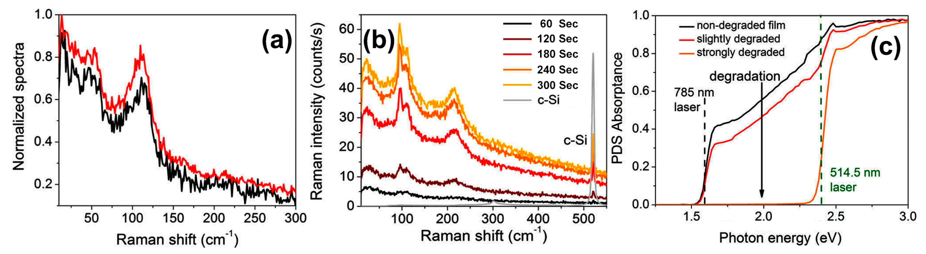
Figure 8.
High-resolution XPS core level spectra of (a) Pb 4f and (b) I 3d when different thicknesses of PbCl2 are deposited on 10.0 nm of MAI. XPS core level spectra of (c) Pb 4f and (d) Br 3d when different thicknesses of PbI2 are deposited on 10.0 nm of MABr [88]. Copyright © 2015, American Chemical Society.

Figure 9.
Thickness (t) dependence of UPS spectra of spiro-MeOTAD on MAPbIBr2. The left panel displays the SECO region and the right panel displays the HOMO region, respectively [94]. Copyright © 2015 WILEY-VCH Verlag GmbH & Co. KGaA, Weinheim, Germany.
Figure 9.
Thickness (t) dependence of UPS spectra of spiro-MeOTAD on MAPbIBr2. The left panel displays the SECO region and the right panel displays the HOMO region, respectively [94]. Copyright © 2015 WILEY-VCH Verlag GmbH & Co. KGaA, Weinheim, Germany.
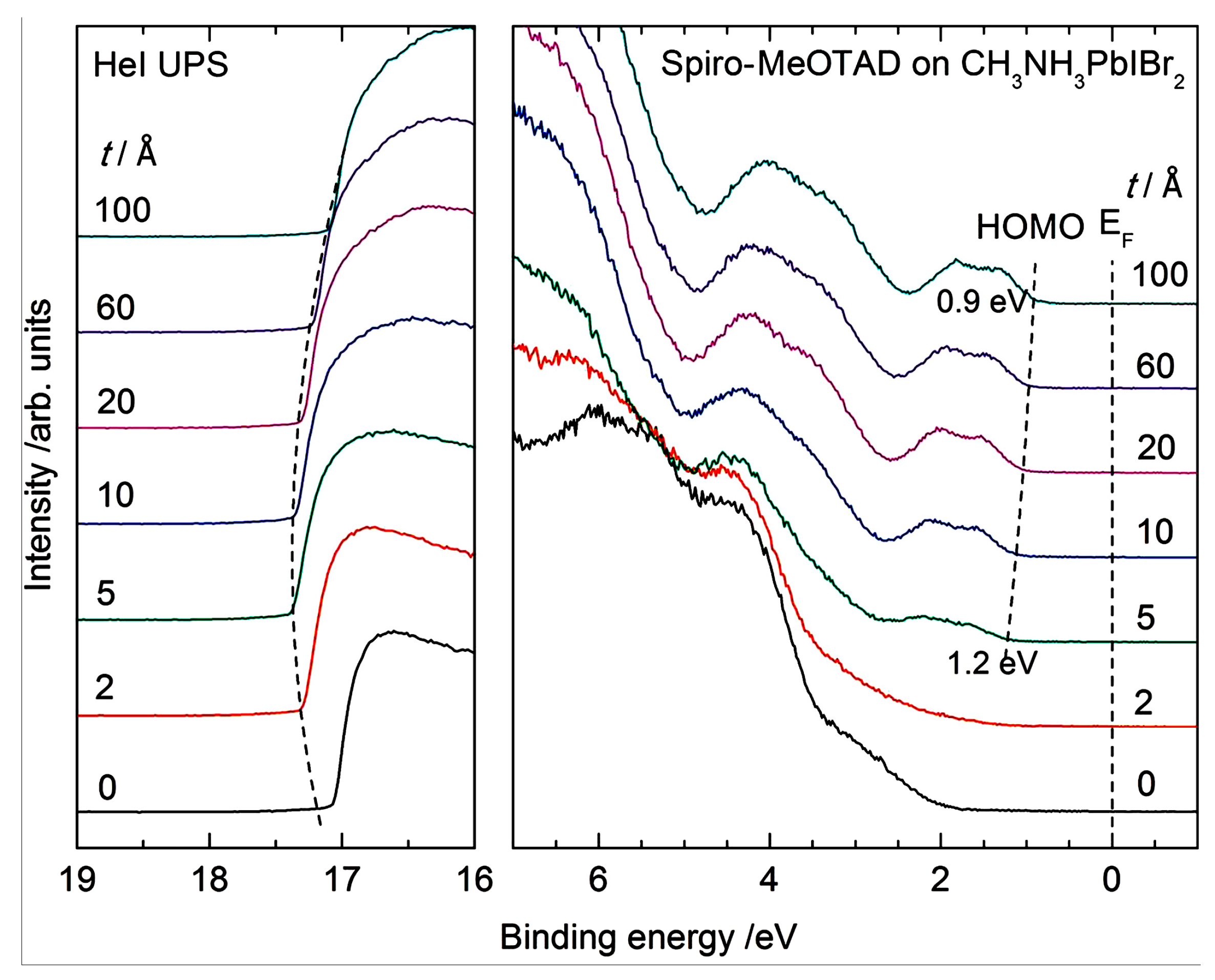
Figure 10.
UPS and IPES spectra of MAPbI3 on sNiOx (black curve) and MAPbI3 on TiO2 (orange curve). The left panel shows the secondary electron cutoff for work function determination. The middle panel shows the He II valence band spectra. The VBM measured with He I is shown in inset. The right panel shows the IPES spectra for the determination of the CBM [95]. Copyright © 2015 WILEY-VCH Verlag GmbH & Co. KGaA, Weinheim, Germany.

Figure 11.
Optical micrographs of hybrid perovskite film (scale bar: 50 μm) from precursor with (a) 0%; (b) 1%; (c) 2%; (d) 5%; and (e) 10% iodine solution (40 mM). (f) Average domain size as a function of iodide loading during fabrication. The average domain size decreases as the iodide loading increases [96]. Copyright © 2015, American Chemical Society.

Figure 12.
Ultraviolet photoelectron spectroscopy (UPS) of perovskite film with (red line) and without (blue line) IPA treatment on ITO glass substrates, i.e., (a) The secondary electron cut-off; (b) the full UPS spectrum using He I radiation; (c) the valence-band region; and (d) X-ray diffraction of perovskite film with and without IPA treatment on ITO glass substrates [113]. Copyright © 2015, Elsevier.

Figure 13.
(a) Schematic image of the laser confocal microscopy and (b,c) the measured spatial PL images from the perovskite films annealed at low and high temperatures, respectively [117]. Copyright © 2015, American Chemical Society.
Figure 13.
(a) Schematic image of the laser confocal microscopy and (b,c) the measured spatial PL images from the perovskite films annealed at low and high temperatures, respectively [117]. Copyright © 2015, American Chemical Society.

Figure 14.
Cross-sectional SEM images of (a) TiO2 (40 wt %-PMMA); (b) TiO2 (nanoparticle); (c) TiO2 (40 wt %-PS); and (d) TiO2 (without polymer) on FTO/cTiO2 substrates. Scale bars are 200 nm, and Wide-angle XRD patterns of (e) PbI2 and (f) perovskite MAPbI3 films deposited on FTO/cTiO2/TiO2 (40 wt %-PMMA) (red line), FTO/cTiO2/TiO2 (40 wt %-PS) (green line), and FTO/cTiO2/TiO2 (no-polymers) (blue line). Symbols of green solid circle (•) and pink star (*) represent the XRD diffraction peak position of PbI2 and CH3NH3PbI3 [128]. Copyright © 2015, American Chemical Society.


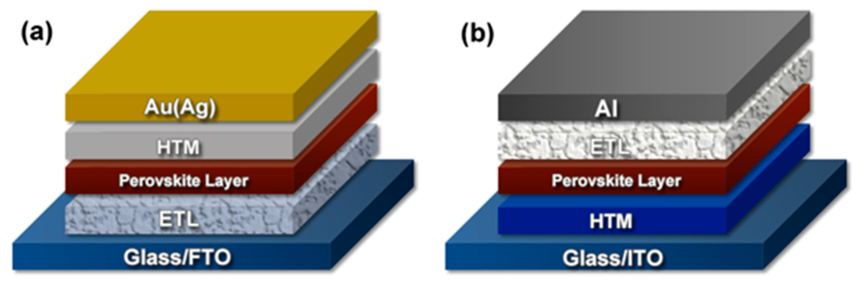
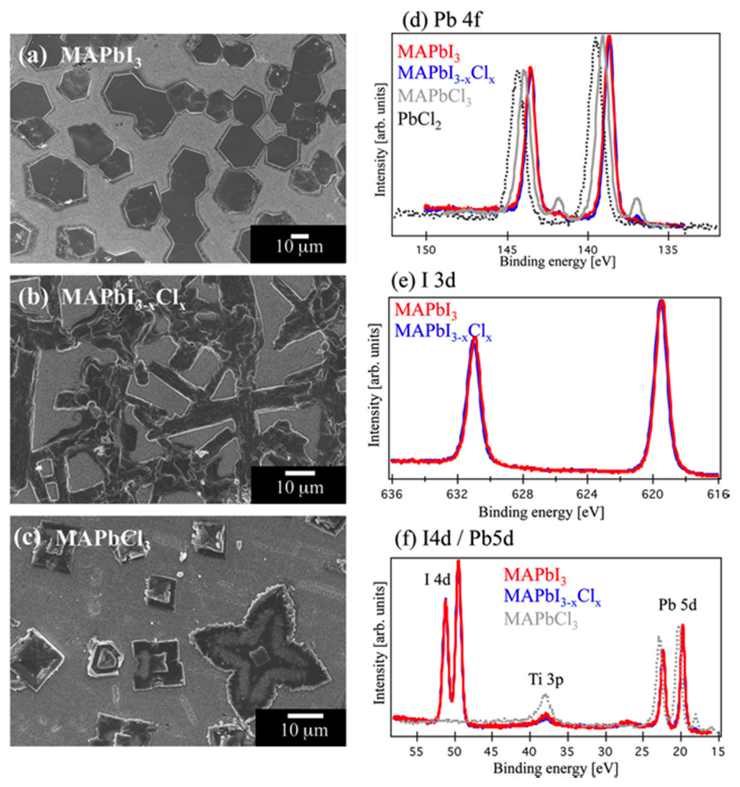
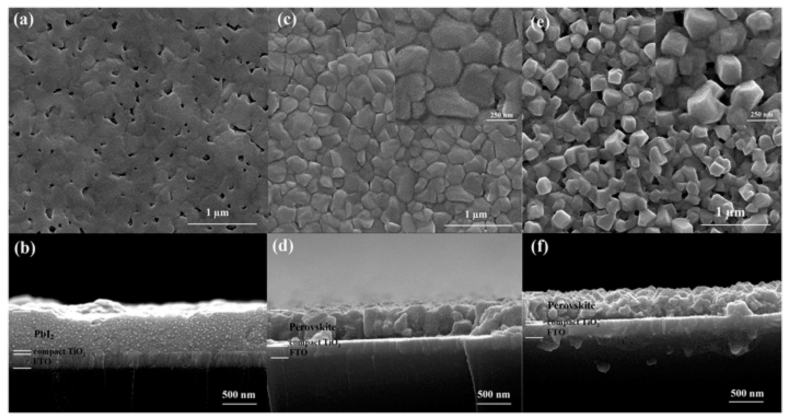
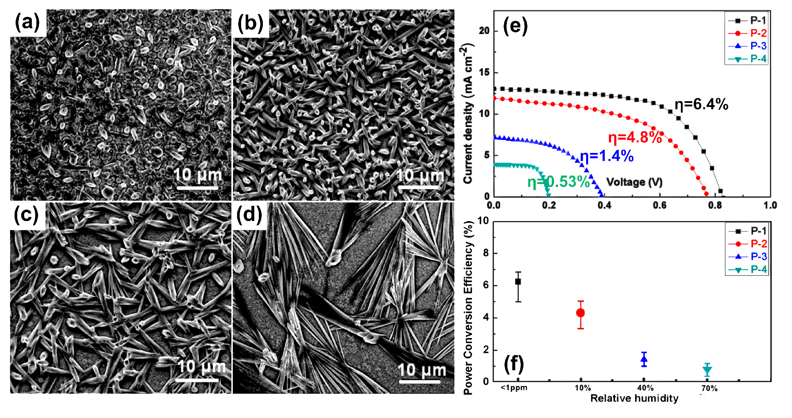
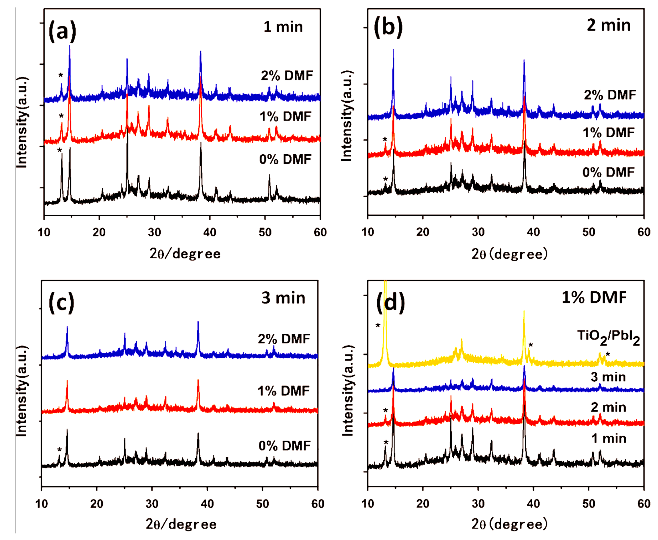
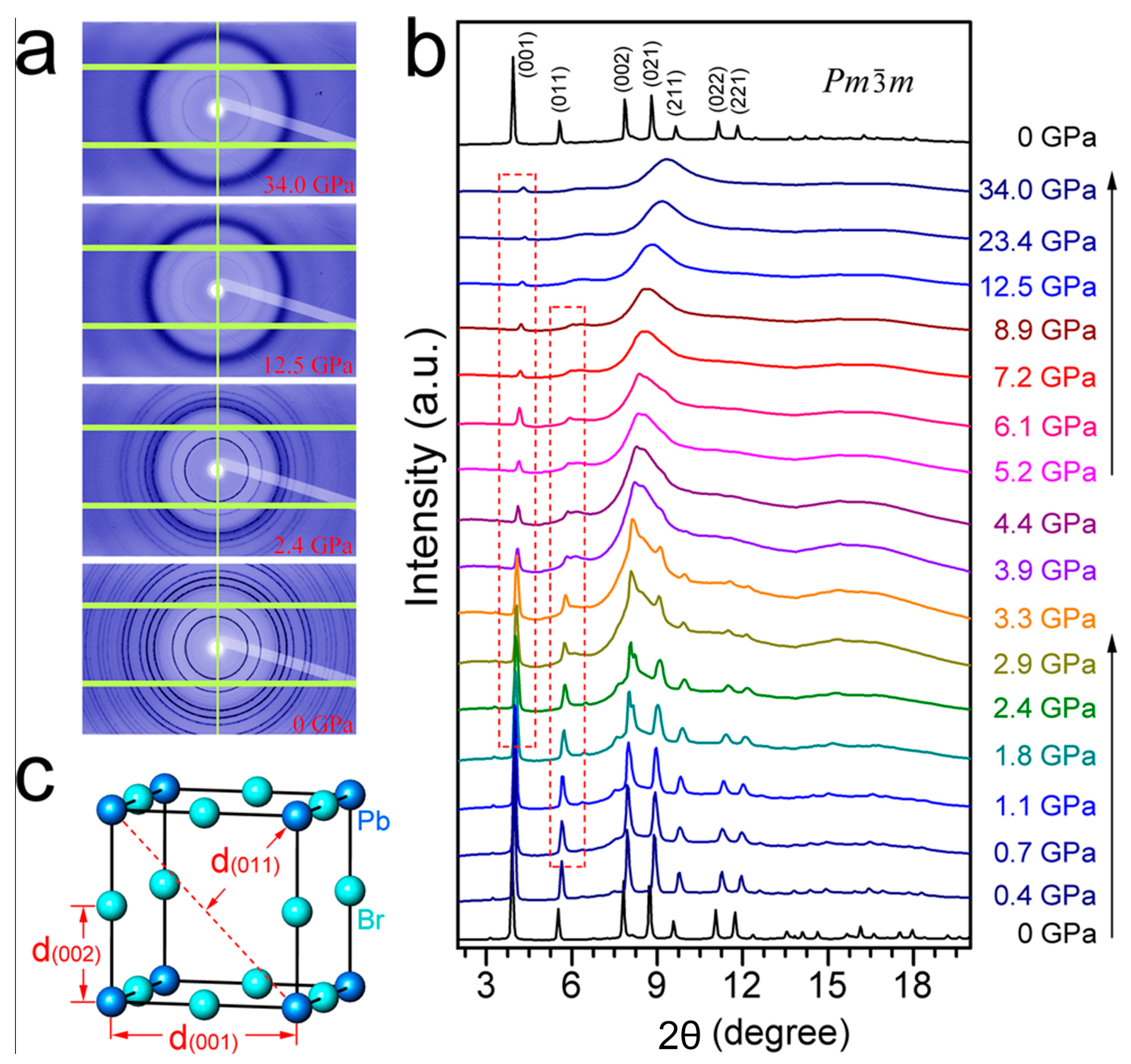
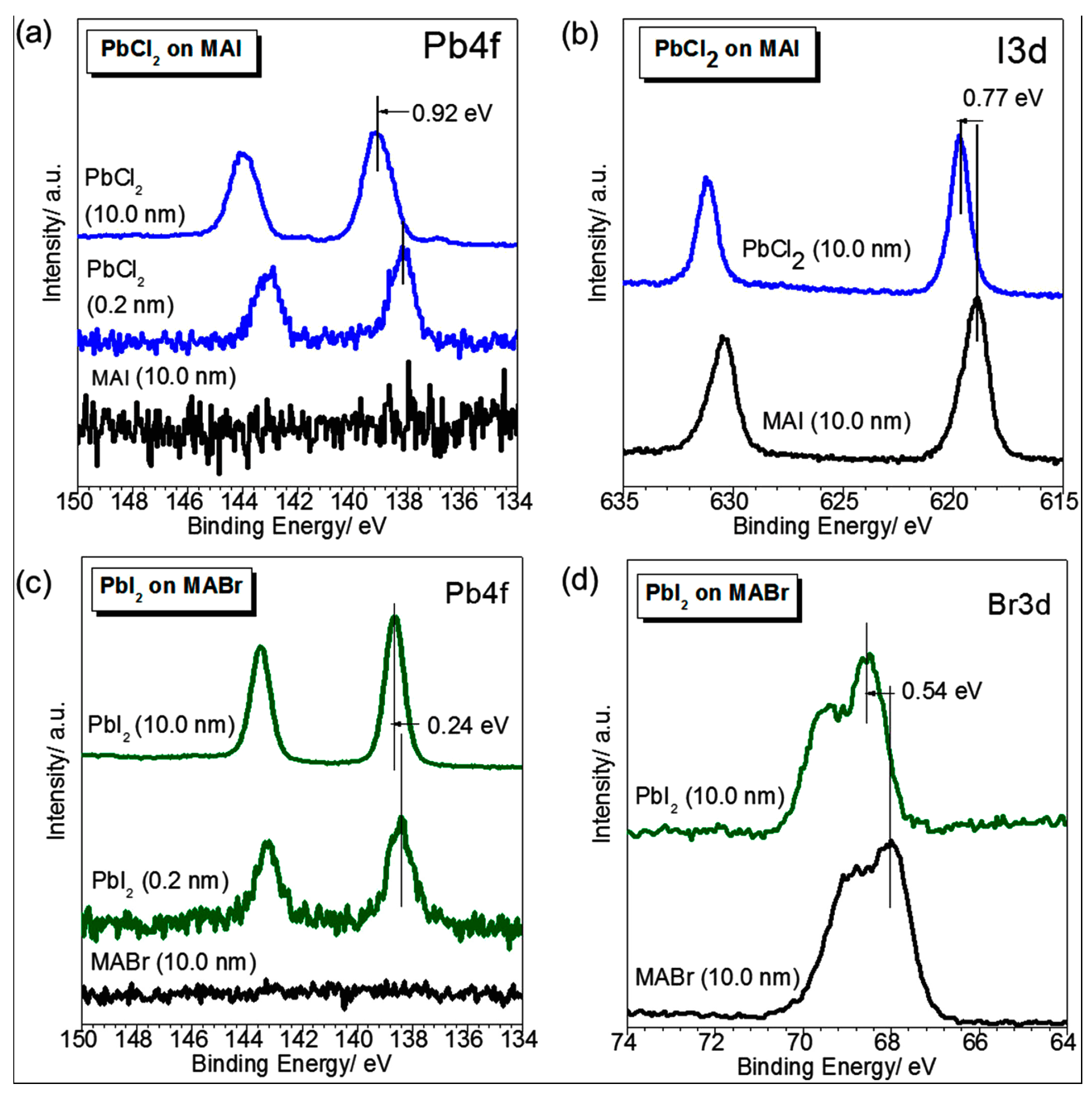
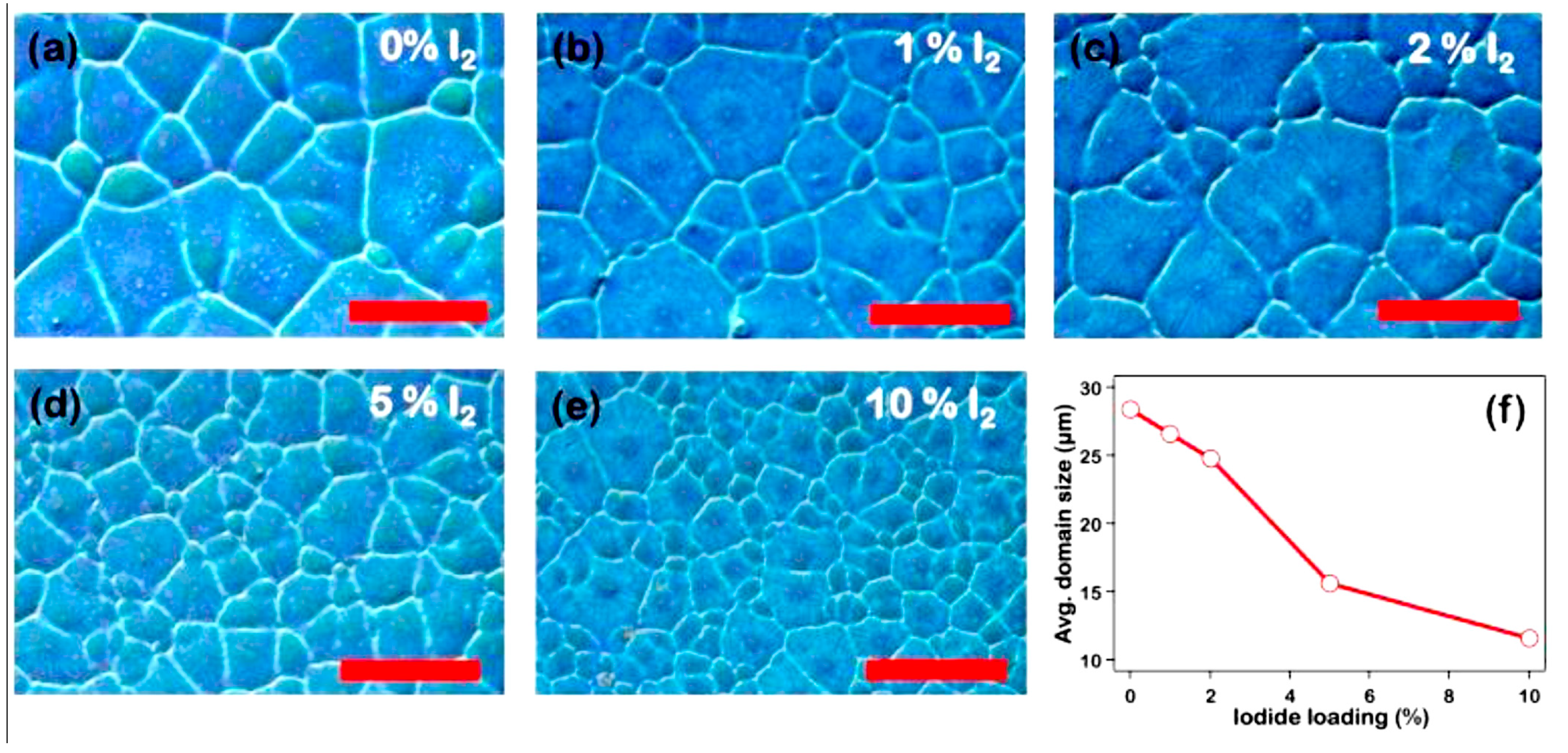
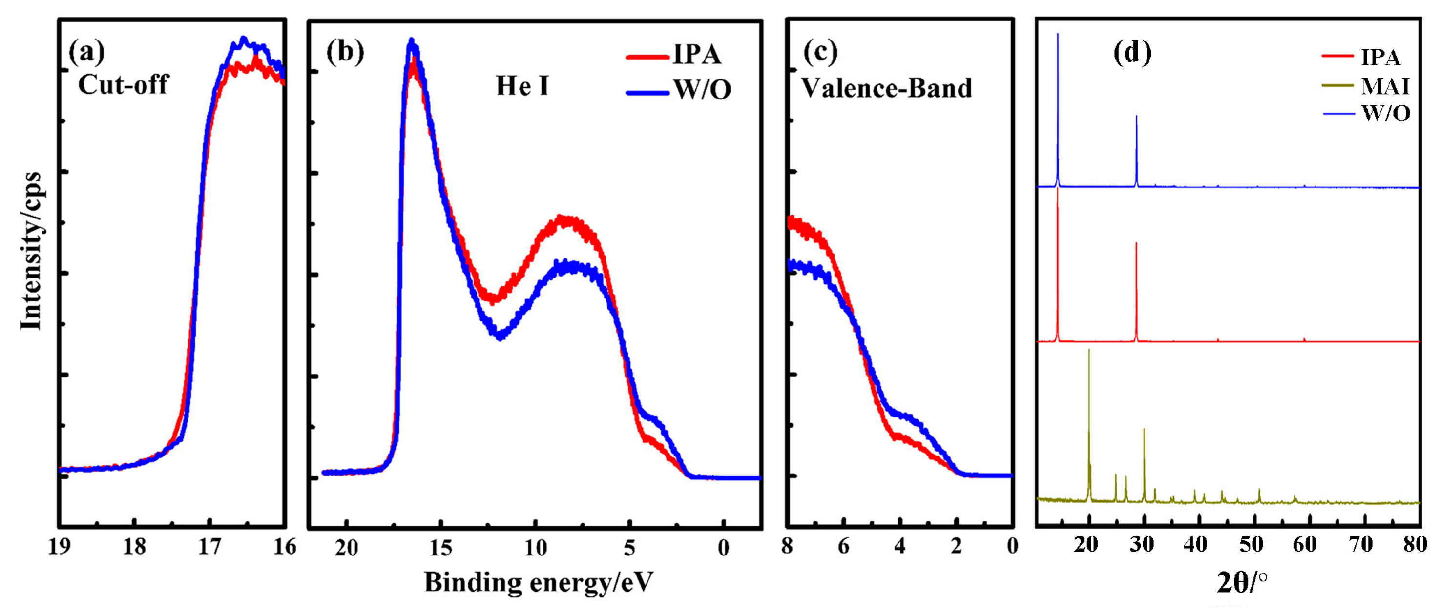
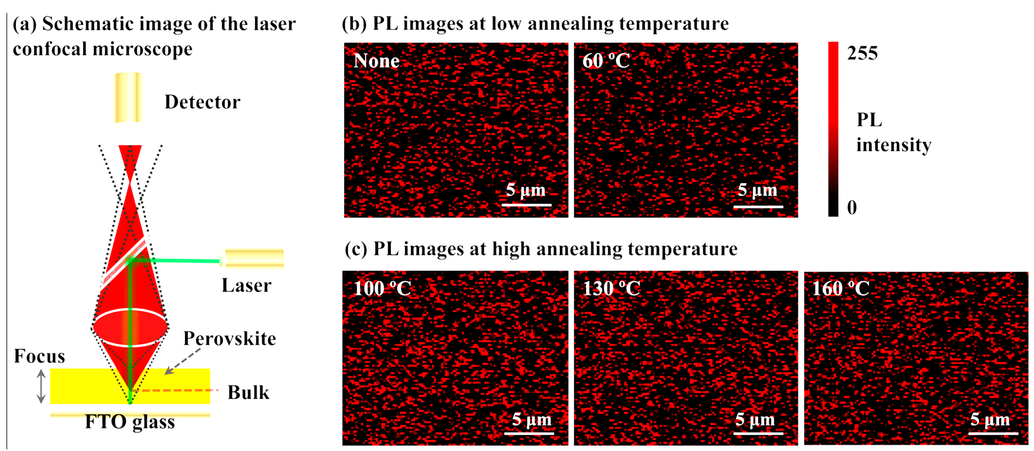
Table 1.
Photovoltaic parameters of perovskite solar cells as a function of PbCl2 concentration [42]. Copyright © 2015, Elsevier, Amsterdam, The Netherlands.
Table 1.
Photovoltaic parameters of perovskite solar cells as a function of PbCl2 concentration [42]. Copyright © 2015, Elsevier, Amsterdam, The Netherlands.
| Precursor Solutions (MA:Pb:I:Cl) | Performance Type | JSC (mA/cm2) | VOC (mV) | FF (%) | PCE (%) |
|---|---|---|---|---|---|
| 1 M PbI2 + 1 M MAI (1:1:3:0) | Average | 3.32 ± 1.87 | 649 ± 311 | 46.3 ± 12.6 | 1.40 ± 0.97 |
| Best | 4.74 | 895 | 56.3 | 2.36 | |
| 0.3 M PbCl2 + 0.7 M PbI2 + 1.6 M MAI (1.6:1:3:0.6) | Average | 15.18 ± 2.55 | 843 ± 40 | 40.4 ± 5.4 | 5.19 ± 1.20 |
| Best | 17.15 | 898 | 45.8 | 7.06 | |
| 0.5 M PbCl2 + 0.5 M PbI2 + 2.0 M MAI (2:1:3:1) | Average | 19.08 ± 1.65 | 979 ± 40 | 55.5 ± 4.1 | 10.41 ± 1.52 |
| Best | 19.9 | 996 | 62.1 | 12.32 | |
| 0.8 M PbCl2 + 0.2 M PbI2 + 2.6 M MAI (2.6:1:3:1.6) | Average | 19.15 ± 0.88 | 965 ± 35 | 57.6 ± 4.0 | 10.68 ± 1.26 |
| Best | 20.1 | 961 | 63.0 | 12.16 | |
| 1 M PbCl2 + 3 M MAI (3:1:3:2) | Average | 18.28 ± 1.16 | 857 ± 87 | 50.4 ± 5.4 | 7.95 ± 1.66 |
| Best | 18.74 | 996 | 57.7 | 10.77 |
Table 2.
Parameters of Devices Annealed under Different Atmospheric Conditions [115]. Copyright © 2015, American Chemical Society.
Table 2.
Parameters of Devices Annealed under Different Atmospheric Conditions [115]. Copyright © 2015, American Chemical Society.
| Solvent | Scan Direction | VOC (V) | JSC (mA/cm2) | FF (%) | PCEmax (%) | PCEave (%) 1 |
|---|---|---|---|---|---|---|
| N2 | Forward | 0.93 | 16.9 | 0.53 | 8.34 | 7.39 ± 0.62 |
| Reverse | 0.91 | 17.1 | 0.55 | 8.55 | 7.59 ± 0.60 | |
| H2O | Forward | 0.95 | 18.7 | 0.51 | 8.99 | 7.50 ± 1.40 |
| Reverse | 0.94 | 18.6 | 0.51 | 8.85 | 7.62 ± 1.14 | |
| γ-butyrolactone (GBL) | Forward | 0.92 | 20.9 | 0.64 | 12.29 | 11.50 ± 0.74 |
| Reverse | 0.92 | 20.8 | 0.65 | 12.47 | 11.32 ± 0.86 | |
| DMF | Forward | 10.91 | 20.2 | 0.62 | 11.29 | 10.47 ± 0.82 |
| Reverse | 0.91 | 20.3 | 0.64 | 11.89 | 10.65 ± 0.70 | |
| DMSO | Forward | 0.93 | 20.9 | 0.68 | 13.21 | 11.89 ± 1.43 |
| Reverse | 0.93 | 20.9 | 0.69 | 13.59 | 12.04 ± 1.27 |
1 Average PCE Values were obtained from 5 to 8 Cells for each type of devices.
© 2017 by the authors. Licensee MDPI, Basel, Switzerland. This article is an open access article distributed under the terms and conditions of the Creative Commons Attribution (CC BY) license (http://creativecommons.org/licenses/by/4.0/).
Share and Cite
MDPI and ACS Style
Zeng, W.; Liu, X.; Guo, X.; Niu, Q.; Yi, J.; Xia, R.; Min, Y. Morphology Analysis and Optimization: Crucial Factor Determining the Performance of Perovskite Solar Cells. Molecules 2017, 22, 520. https://doi.org/10.3390/molecules22040520
AMA Style
Zeng W, Liu X, Guo X, Niu Q, Yi J, Xia R, Min Y. Morphology Analysis and Optimization: Crucial Factor Determining the Performance of Perovskite Solar Cells. Molecules. 2017; 22(4):520. https://doi.org/10.3390/molecules22040520
Chicago/Turabian StyleZeng, Wenjin, Xingming Liu, Xiangru Guo, Qiaoli Niu, Jianpeng Yi, Ruidong Xia, and Yong Min. 2017. "Morphology Analysis and Optimization: Crucial Factor Determining the Performance of Perovskite Solar Cells" Molecules 22, no. 4: 520. https://doi.org/10.3390/molecules22040520